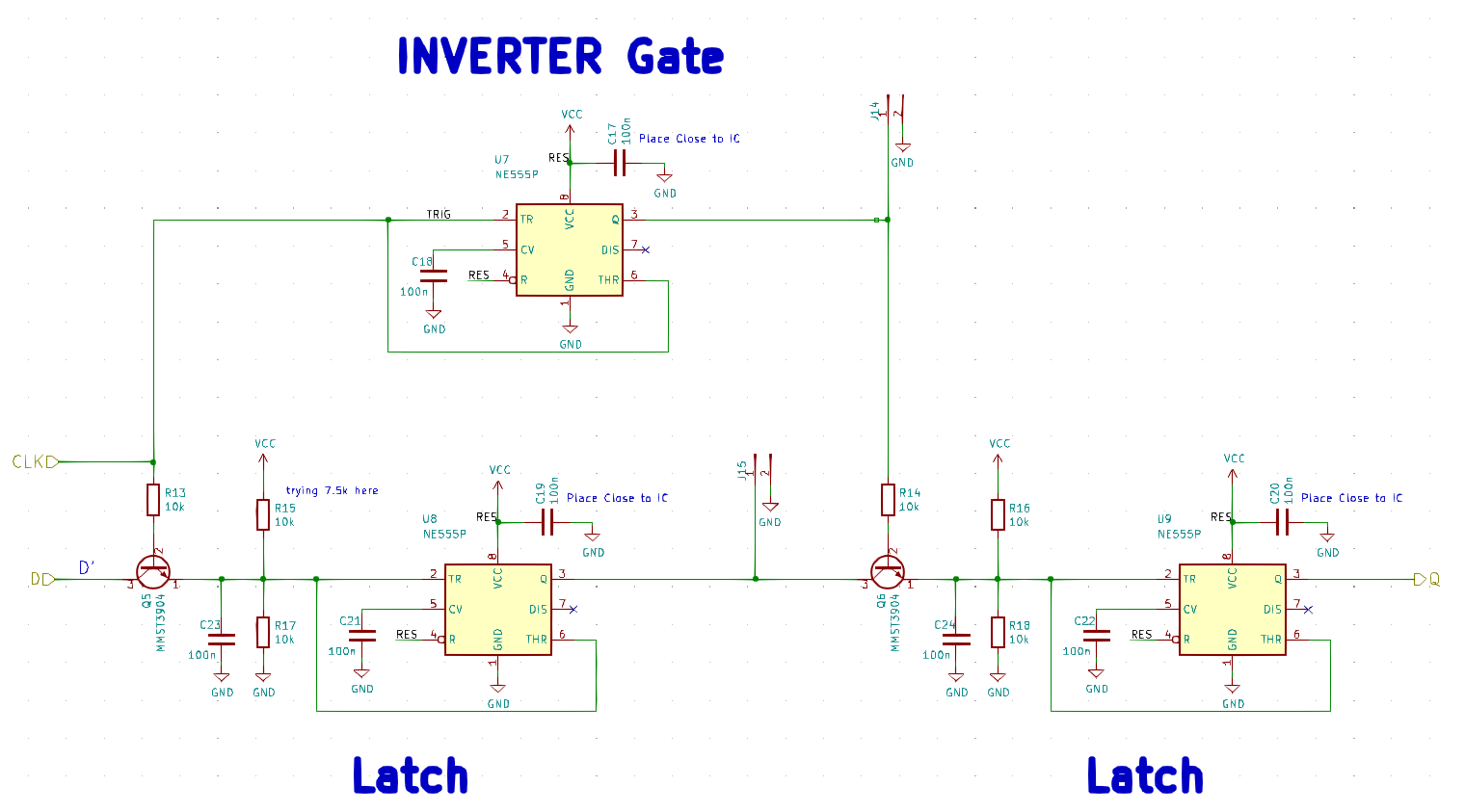
This circuit induced several headaches… As a refresher the validation schematic and PCB are shown below. The circuit initially did not work; this was caused by an incorrect bjt footprint (flipped base– emitter pads).


After this change the flip flop worked but only for slower clock signals… This is because pin 2 of the 555’s in the latch circuits is essentially left floating when the BJTs are closed, creating an RC time constant of ~1ms. Basically, the trigger wasn’t resetting quickly enough. Reducing C23 and C24 to 10nF solved this issue, I could probably go lower still but for now this value seems consistent. I also reduced the base resistors to 5k which seemed to improve the reliability.
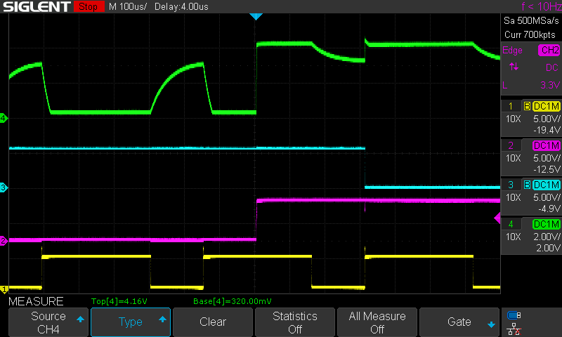
The next issue was that the circuit was intermittently triggering on rising edges instead of falling edges. The scope capture below contains all the I/O of the first latch. Channel 1 is the clock input, Channel 2 is the data, Channel 3 is the latch output (note we expect this to be !data), and Channel 4 is the trigger.

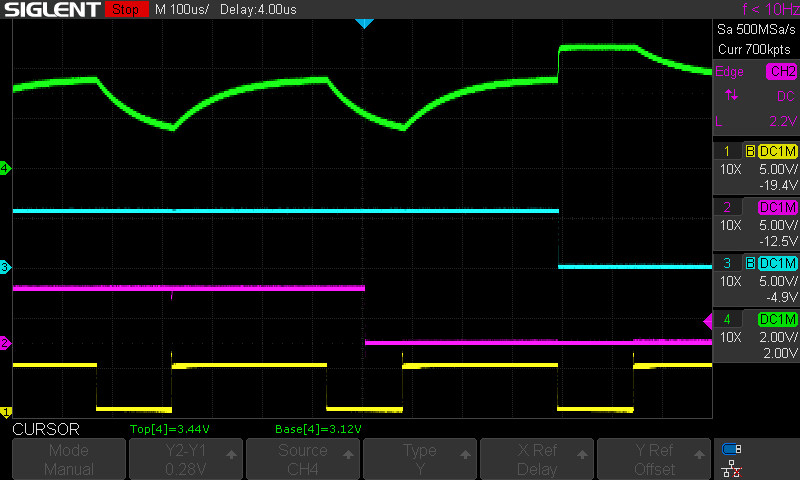
To solve this, I tweaked the R17 – R15 voltage divider. Changing R15 to 7.5k pulls the voltage up by 400mV which then solved my issue. Note that this makes my system more susceptible to noise, since now I only have 600mV of +swing before the 555 is triggered. Below is the corrected circuit, same probe points as prior capture.

Just as a summary the following changes were made for the eval board to work as expected.
- Fix npn footprint
- Change base resistors to ~5k
- Change voltage divider upper resistors to 7.5k
- Reduce capacitors C31/C32 to 10nF (perhaps a bit lower still)
 Jesse Farrell
Discussions
Become a Hackaday.io Member
Create an account to leave a comment. Already have an account? Log In.