 Jesse Farrell
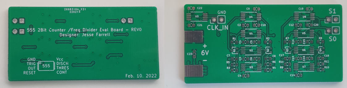
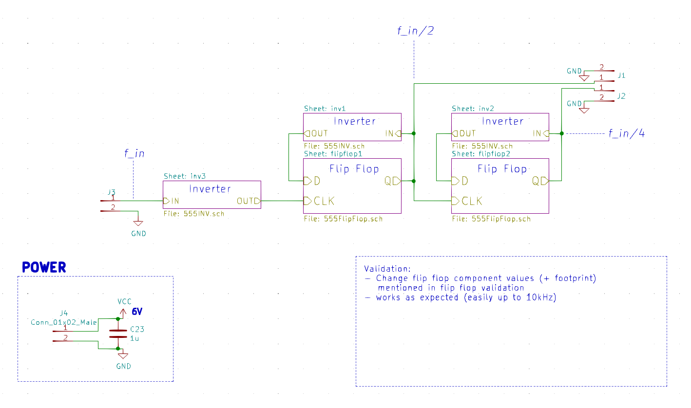
This circuit worked as expected, but the changes mentioned in flip flop validation needed to be made. The schematic (mostly just hierarchical blocks) and pcb are shown below.
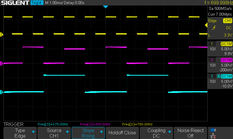
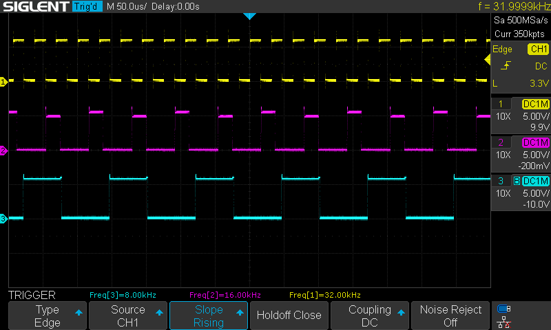
The validation board worked up to ~32kHz after which the output pwm became distorted and missed pulses. Scope captures below with the maximum and typical operating frequency.
Discussions
Become a Hackaday.io Member
Create an account to leave a comment. Already have an account? Log In.