 Jesse Farrell
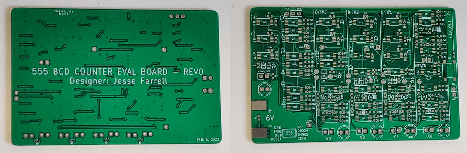
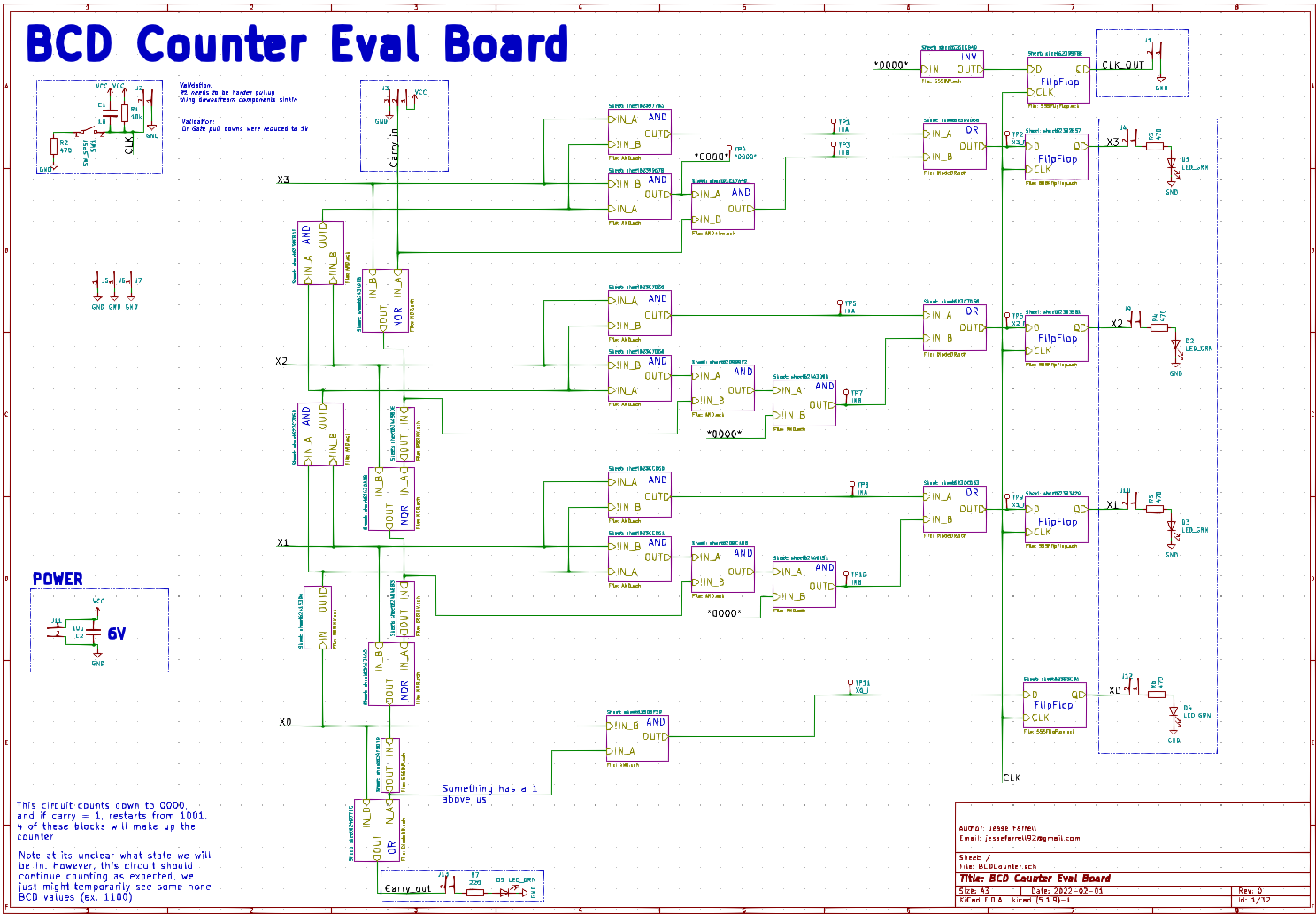
The BCD counter schematic and PCB is shown below.
The circuit worked as expected after correcting the flip flop elements with the changes mentioned in a previous log. Note that this circuit boots into a potentially invalid state, outside the BCD range 0-9. This was anticipated and should be managed by the circuit.
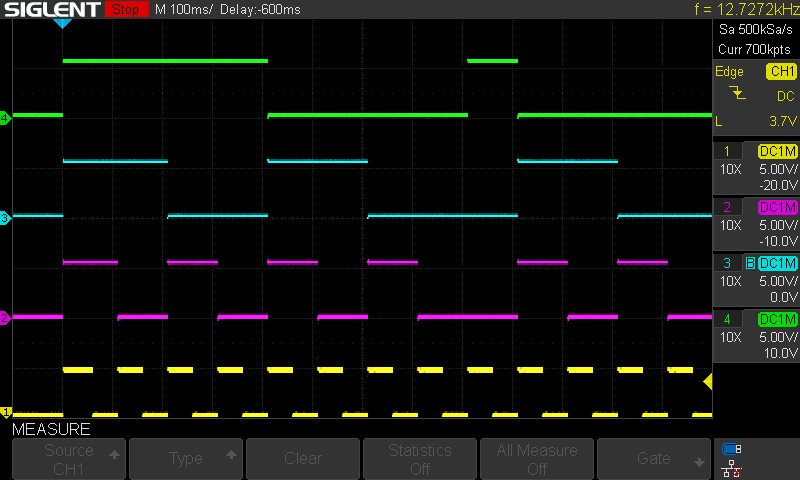
Below is a capture of the waveform powered up with the carry in bit held high. Notice as expected we booted into an invalid state (0b1111 = 15), but the next time the counter rolls over it starts at 9. The scope waveforms are organized MSB -> LSB.
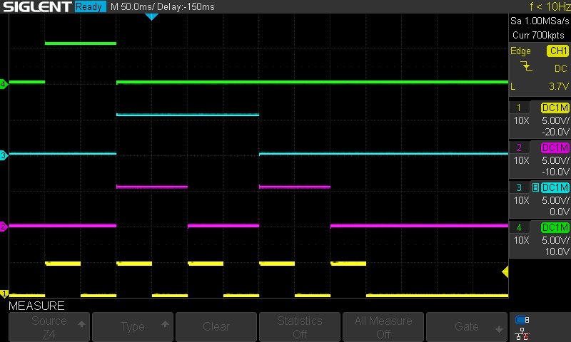
Next testing the circuit with the carry in bit = 0, we expect no roll over when the counter hits 0. A capture of this is shown below. As expected when there the carry in bit is 0, the counter doesn’t rollover.
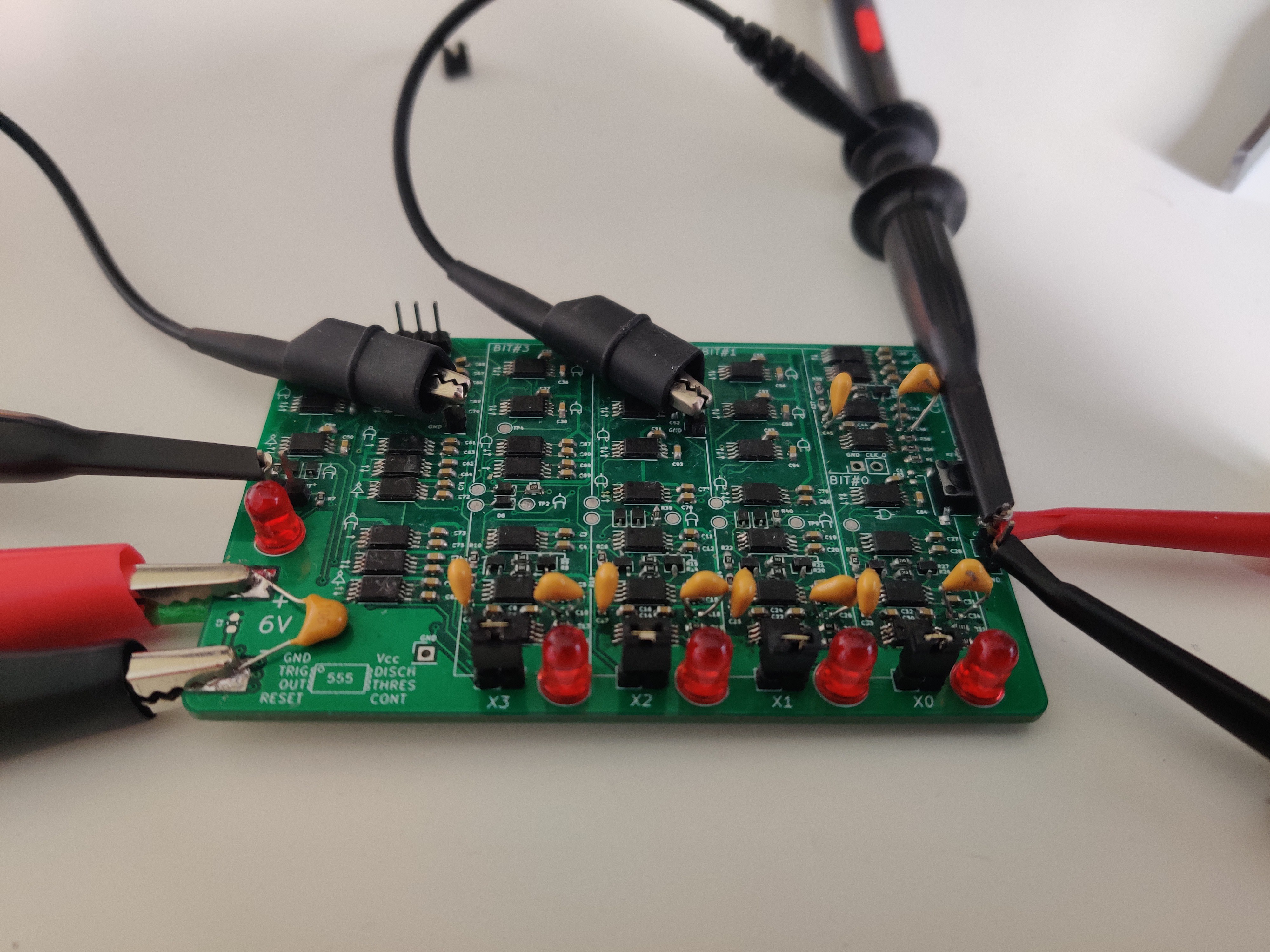
After some usage the solder joints on the SMD-THT bodge job (see below) began to cause some issues. Both the CLK_OUT functionality and CARRY_OUT pins were verified but no captures were taken. CLK_OUT is pulled low when all bits in the counter are 0. CARRY_OUT is high so long as any of the bits are 1.
It might be a good idea to add a buffer between the OR gates and the Flip flop inputs. If a 555 and gate is used a reset functionality could be added to help mitigate the invalid starting state previously mentioned.
Discussions
Become a Hackaday.io Member
Create an account to leave a comment. Already have an account? Log In.