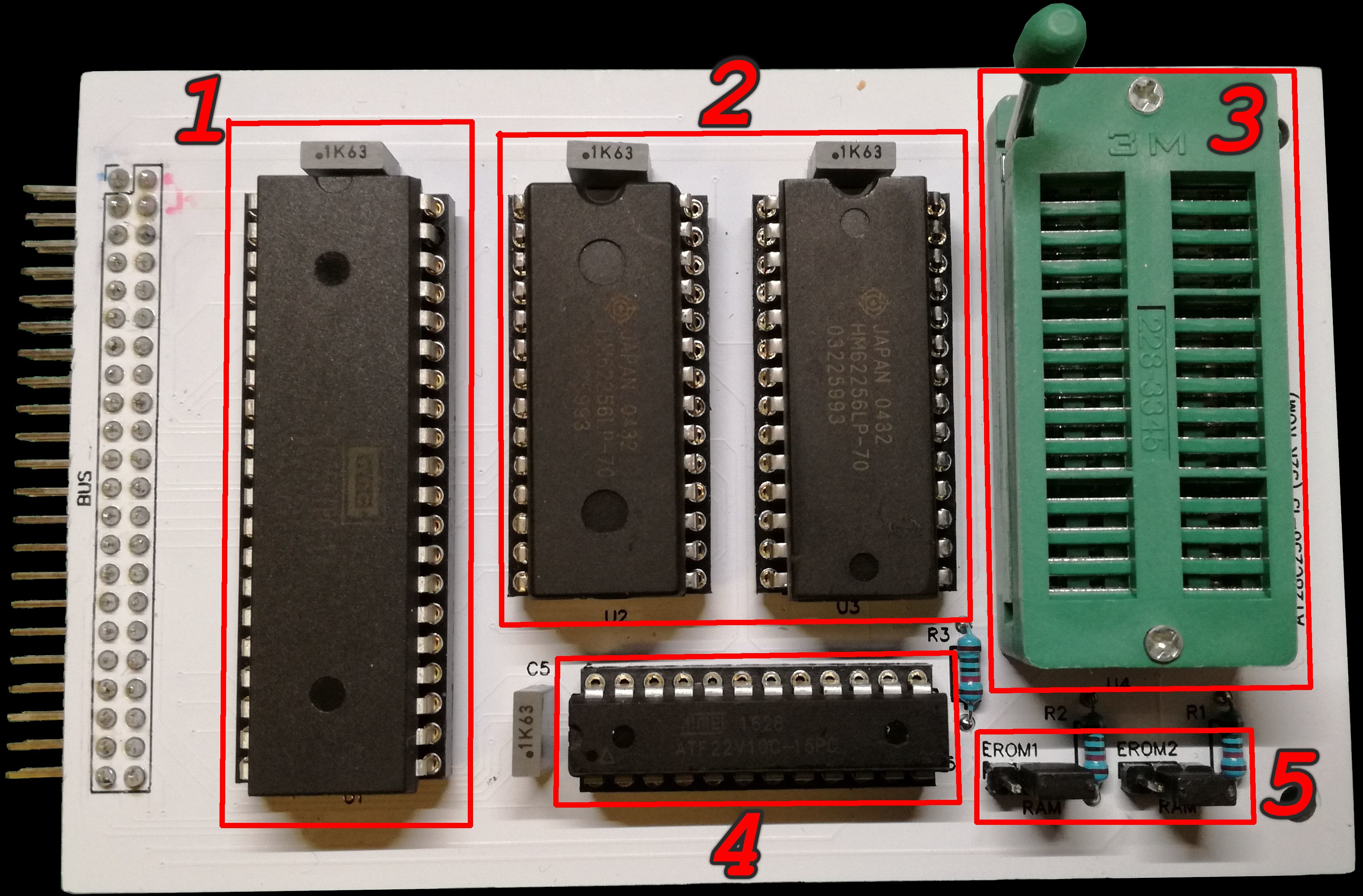
The CPU board hosts:
- the CPU (1)
- the RAM (2)
- the (EEP)ROM (3)
- the PLD (4)
- jumpers to configure memory mapping (5)

In this board prototype I forgot to add a jumper in order to manually select the ROM banking (RAM14).

I will add another jumper for this scope in the next revision.
Schematics: here
CPU (1)
The CPU is the WDC W65c02s processor and it has many improvements against the old MOS 6502:
- full static core (we can stop the clock in LOW or HIGH state without losing the internal state)
- 70 instructions (56 on MOS 6502)
- 16 addressing modes (13 on MOS 6502)
- max 14 Mhz clock (2 Mhz on MOS 6502)
- supply voltage from 1.8 to 5 volts
- low power consumption
Datasheet: here
RAM (2)
64Kb of static RAM are provided by two HM62256LP-70.
Datasheet: here
ROM (3)
A ZIF socket to host the 32Kb AT28C256 EEPROM.
Datasheet: here
PLD (4)
All the system 'glue logic' is managed by an ATmel ATF22V10C-15.
Datasheet: here
Memory configuration (5)
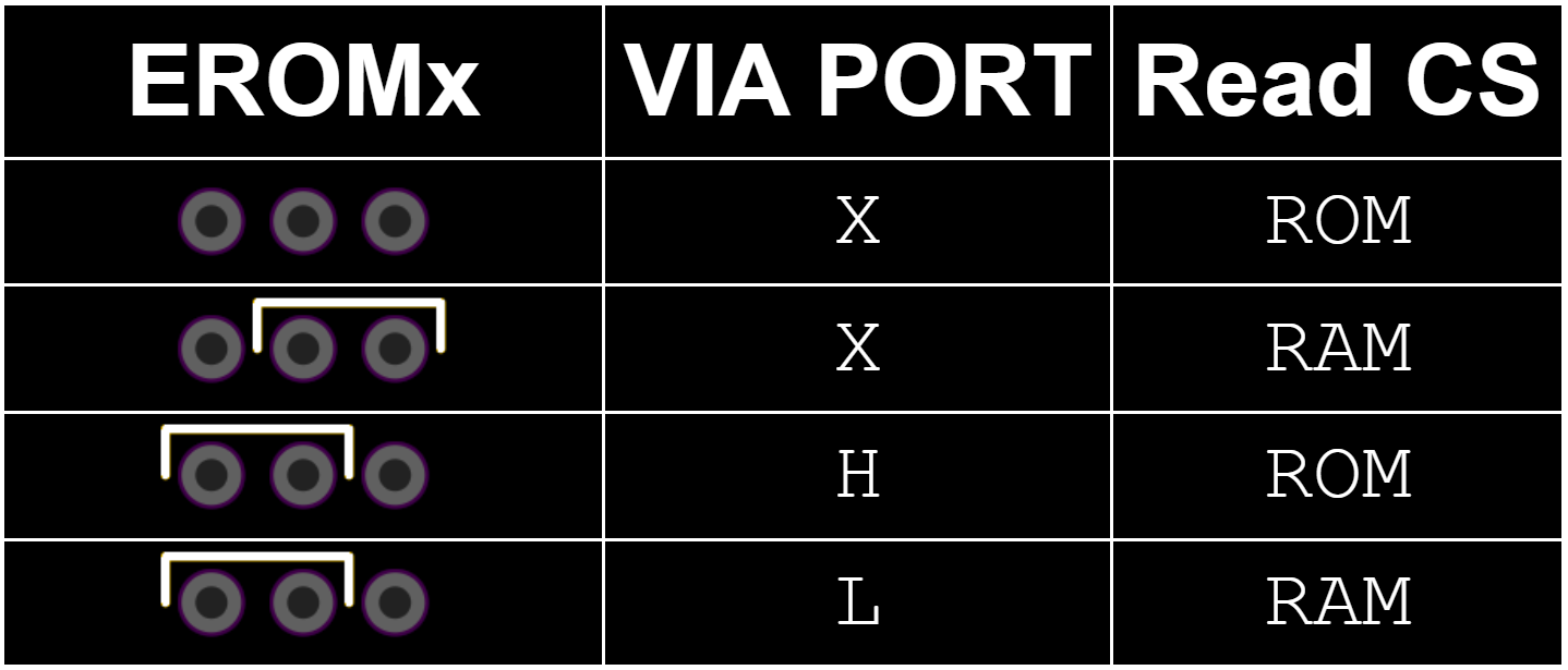
The jumpers can be used to control what to read at address ranges A000-BFFF (EROM1) and E000-FFFF (EROM2).
You can exclude and override the respective EROMx signals generated by one of the VIA (that can be programmatically used to control the configuration).

Ciao!
 padnest
Discussions
Become a Hackaday.io Member
Create an account to leave a comment. Already have an account? Log In.