The Fujitsu Futro S900 is a nice compact thin client, marketed until 2013. It is based on the AMD G-series of APUs (accelerated processing units), bean counter speak for a combination of CPUs and GPUs in a single package.
During the time of manufacture of the S900 there where three APU variants available:
- G-T40N: Single core CPU, 1 GHz clock
- G-T44R: Single core CPU, 1.2 GHz clock
- G-T56N: Dual core CPU, 1.65 GHz clock
I was able to test the hack I describe here on the T40N variant of the S900 as well as the T56N variant. Although the latter is much more powerful it has the disadvantage of requiring a fan.
The S900 thin clients are based on a similar motherboard design by Fujitsu which was targeted at the inustrial control and digital signage market.
Due to this it has a lot of connectivity. It sports 2 real 16550 COM ports. There is a PCI 33 MHz 2.3 slot inside, two PCIe lanes are available on a PCIe x1 connector with non-standard pinout. Thanks to ingenious design connecting regular PCIe x1 cards here shorts out the power supply. The pinout is available for your reference in the technical documentation (see "TechNotes_V3.1_Mini-ITX_D3003-S.pdf" in the Files section).
All these boards had the base name "D3003-XYY". In case of the T40N S900 it is the D3003-D12 variant. This board was never sold as a stand-alone product (at least to my knowledge), whereas the D3003-Sxx variants where available to OEMs.
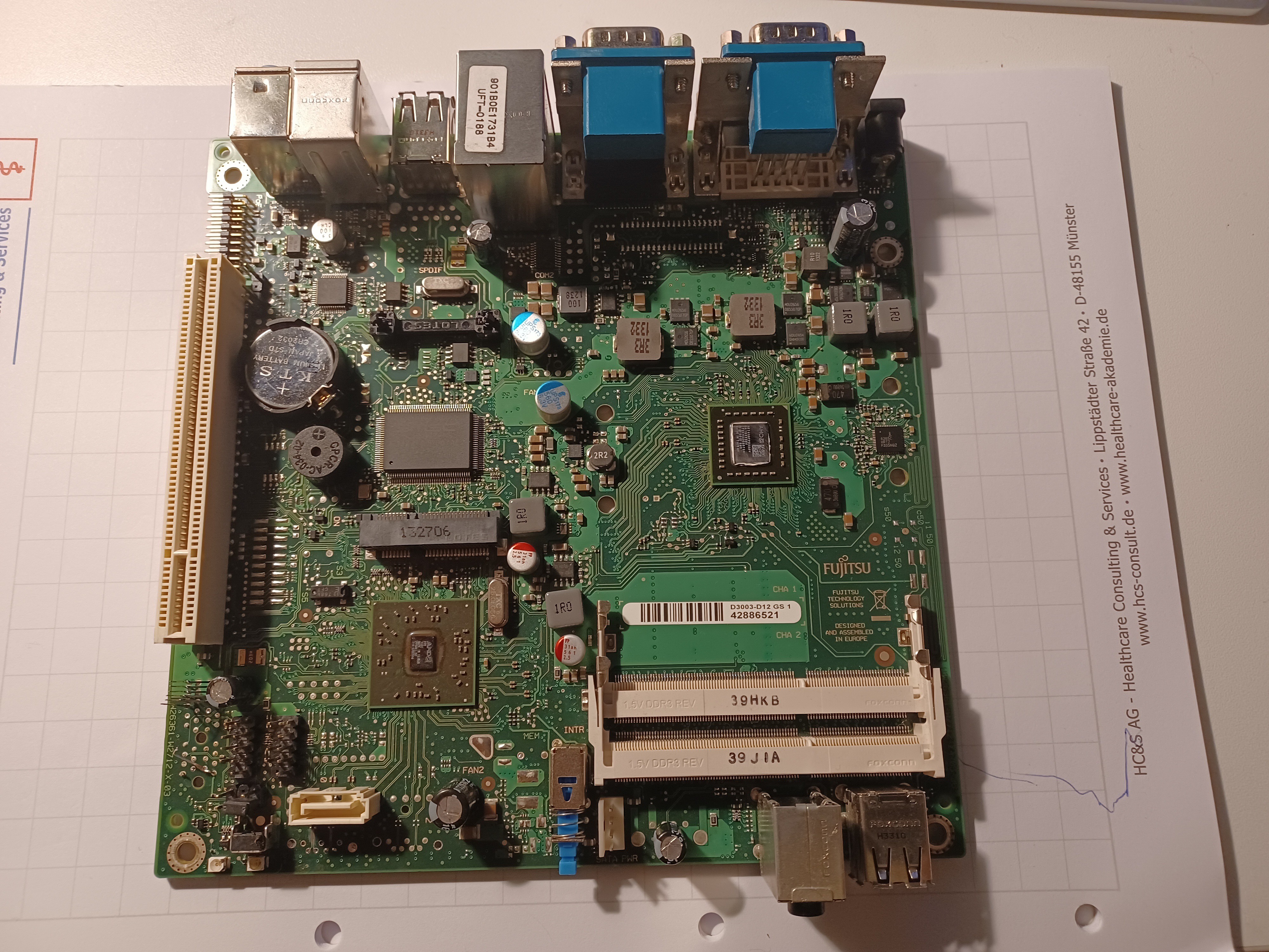
The D3003-D12 board comes, in addition to a mSATA slot, with footprints for 3 SATA jacks, marked 0 - 2, where only jack 0 is populated. That got me thinking ...
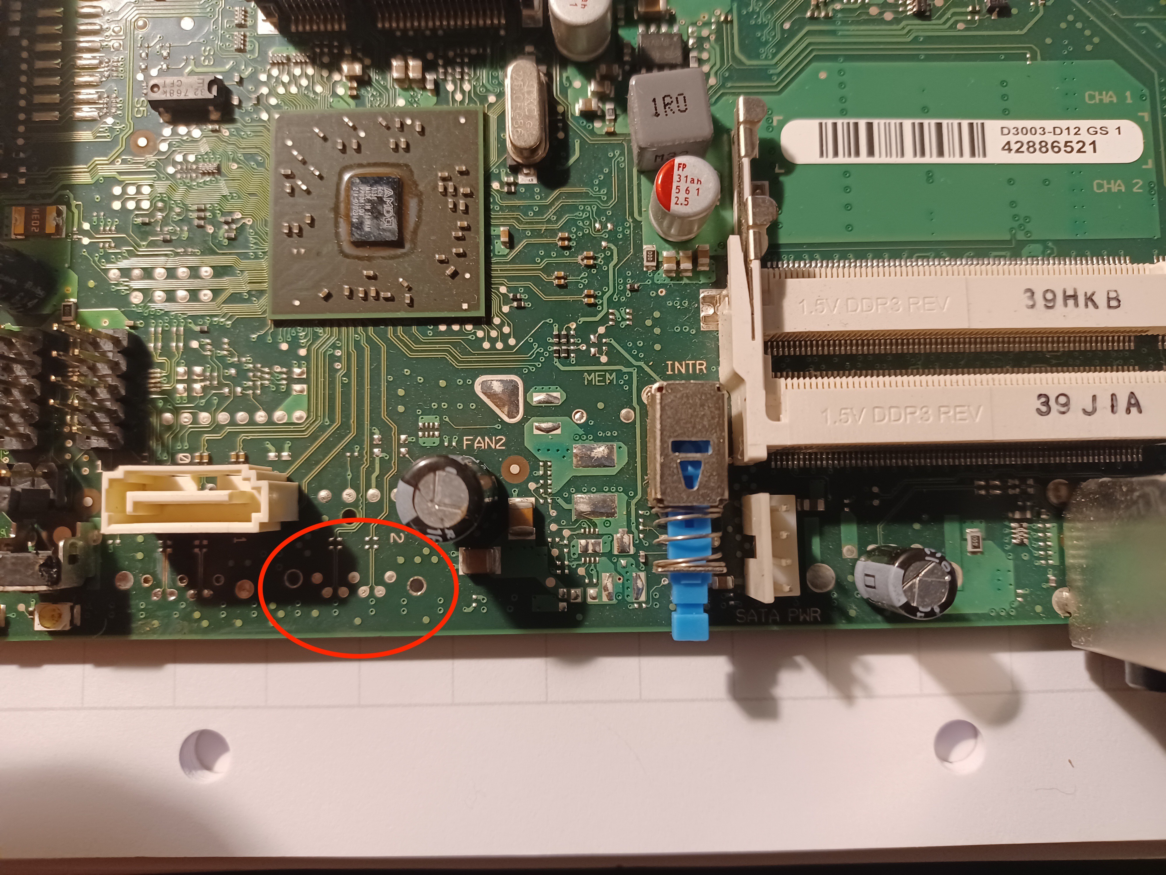
It is obvious that the base hardware comes with the capability hardware-wise to connect more than one external SATA drive.
So I bought some SATA receptacles and soldered them in and added the series capacitors for the data lines. But unfortunately the BIOS was crippled, it was not able to recognise the second port. Frustrated I set the project aside.
Some time later I was surfing the Fujitsu web site and I found BIOS files for D3003-Sxx boards. That got me thinking again ...
I went down a rabbit hole by trying to use the supplied BIOS upgrade software which refused to work on the wrong hardware. First I identified the BIOS ROM chip by using a USB microscope:
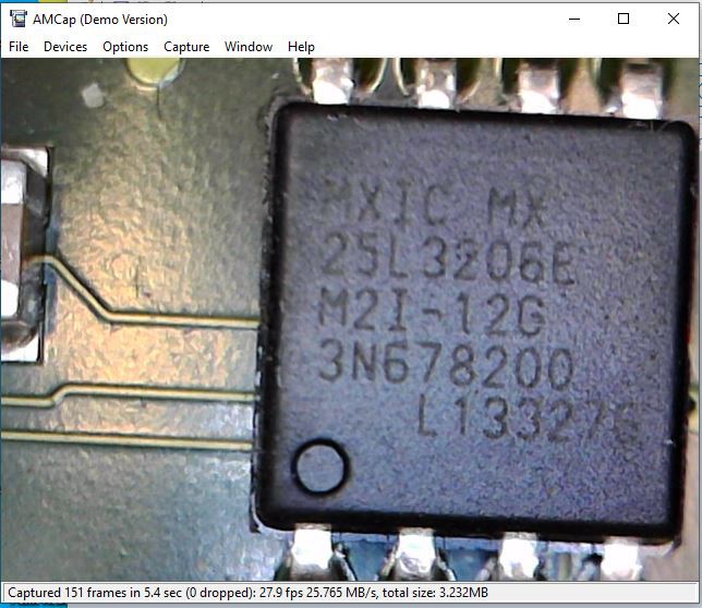
It's a Macronix MX25L3206E 32 Mbit serial flash chip. I desoldered the BIOS chip and read it out with my TL866.
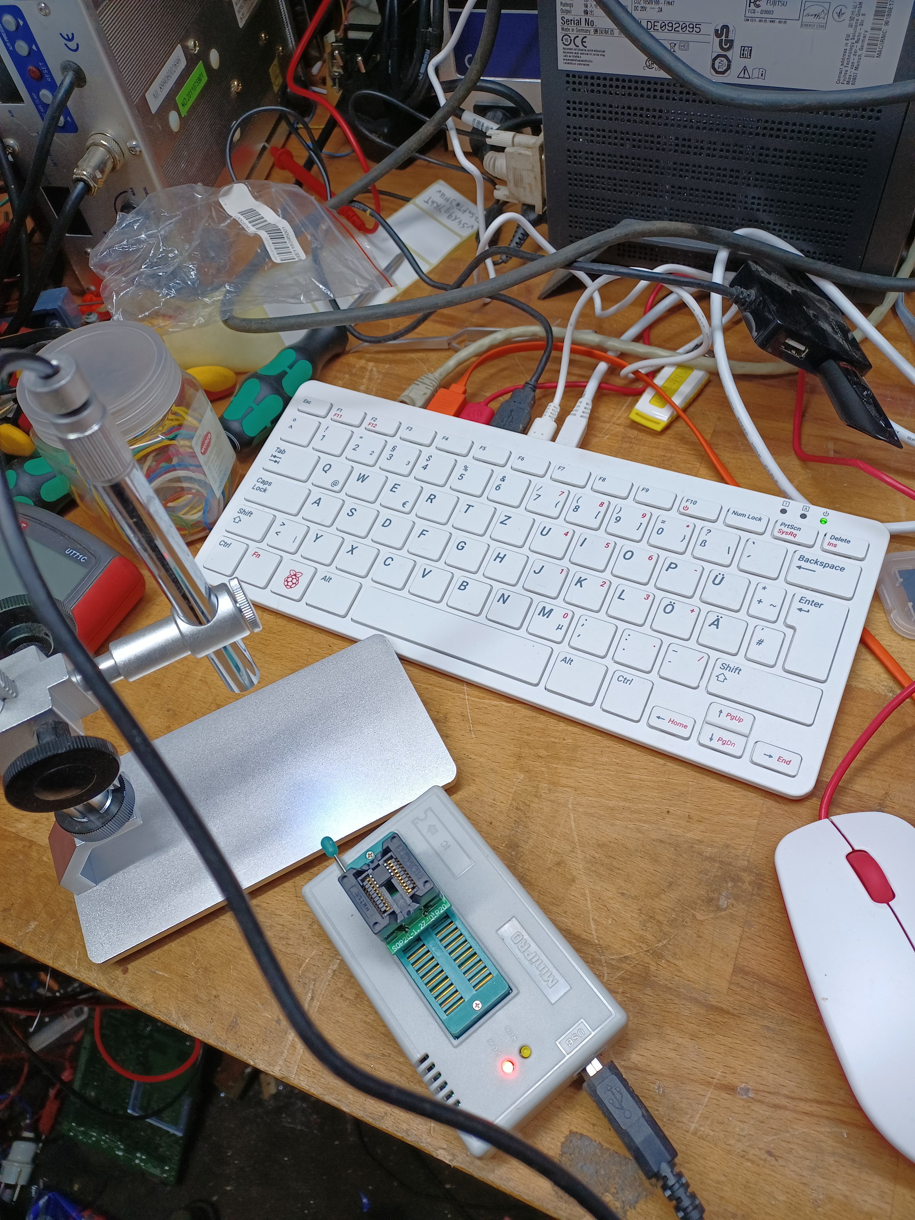
Now I had the contents of the flash chip. The BIOS upgrade package downloaded at Fujitsu contained a *.UPD file with a size of 4.096 MB. At first I thought that this file contains additional information regarding the target system, but actually it is a plain binary.
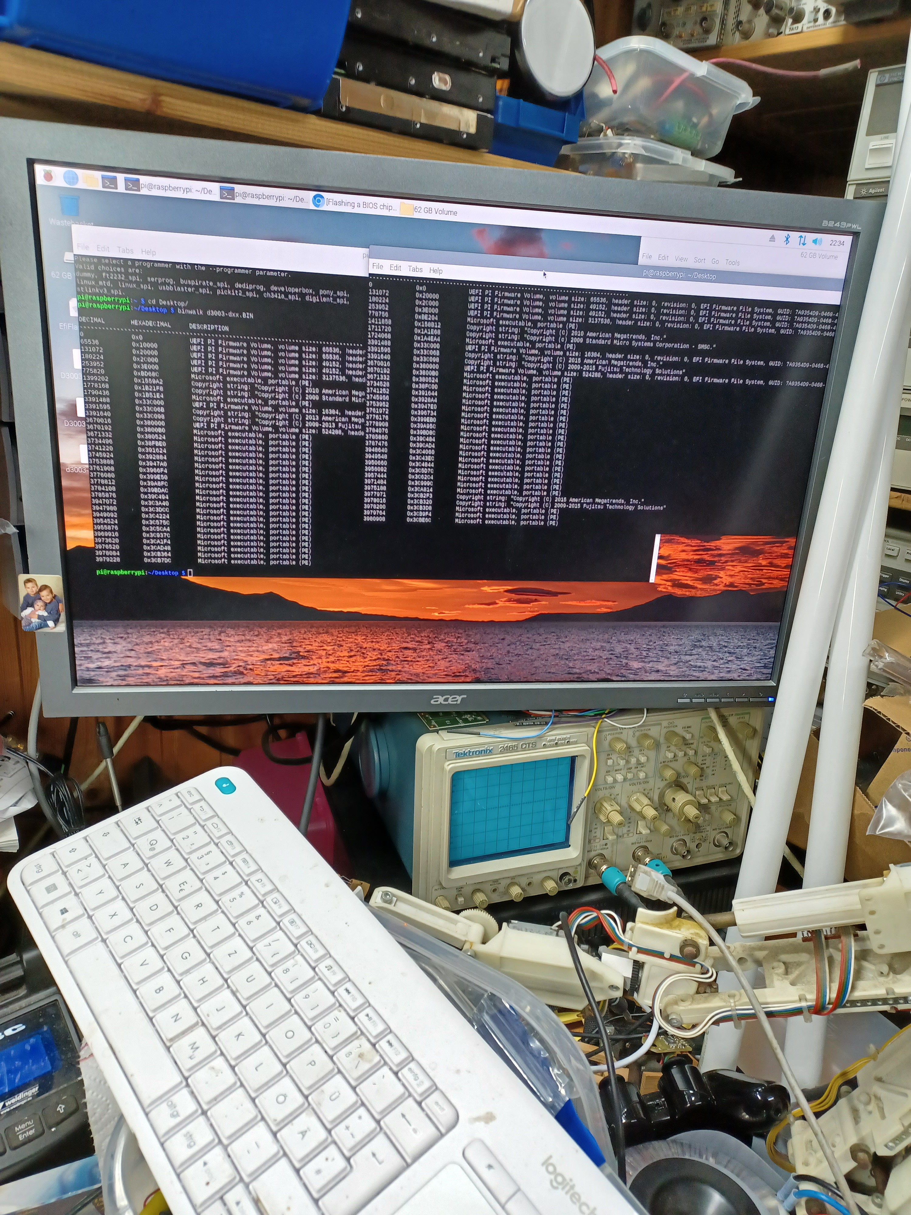
I used the utility "binwalk" to analyze the contents of the read-out flash chip and the *.UPD file from the upgrade package, and they had the same sections at similar addresses:
So I decided to burn the *.UPD file to the BIOS flash ROM. Using the TL866 did not work out, programming always ended with verification errors and there where no bytes actually written. The TL866 seems nice, and it is widely recommended on maker-related web sitest, but in my opinion the device support is flakey and can't be trusted upon as this happened more than once when I needed a generic memory device programmer.
I was looking for another option, when I remembered the "flashrom" utility. I downloaded a copy of "SystemRescueCD" which contains flashrom, made a bootable USB stick and powered up the S900 after soldering the flash ROM back in.

I was happy to see that flashrom was able to make the programming hardware work and detected the ROM.
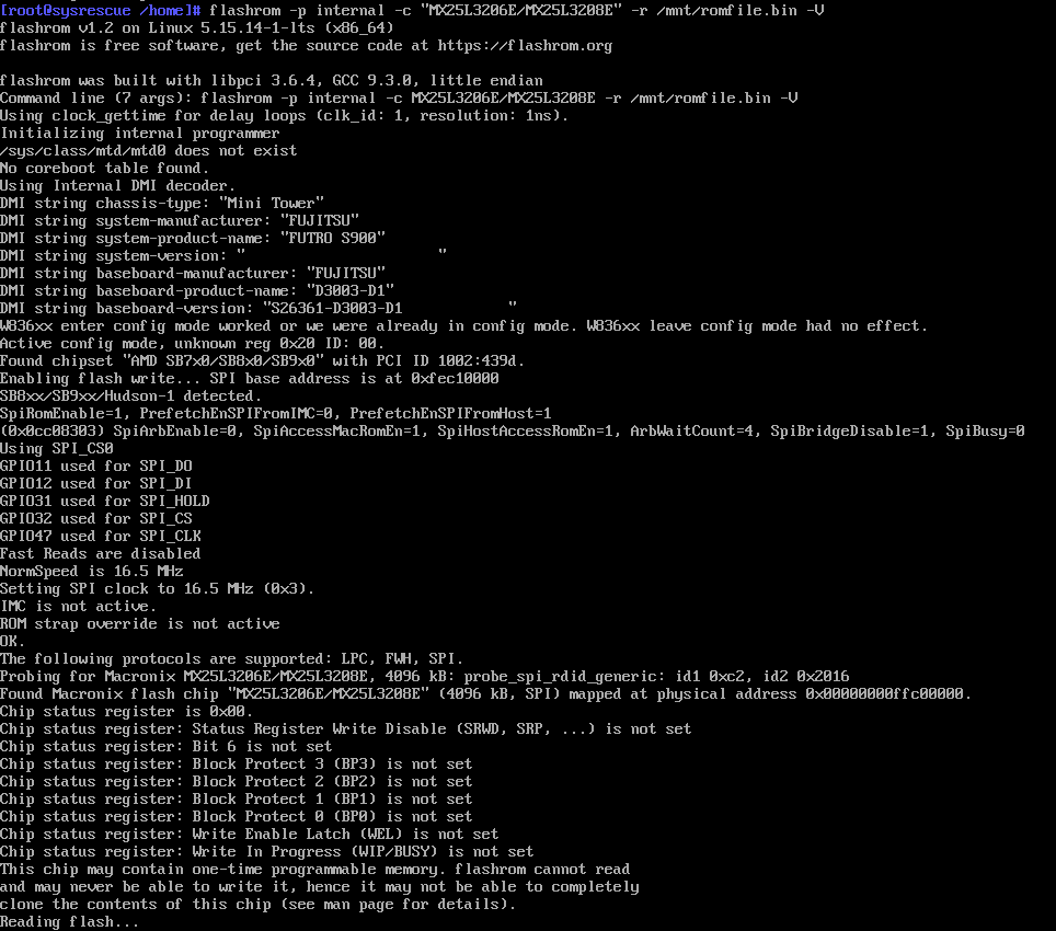
First I made a backup...
Then - fingers crossed - I dared to flash the *.UPD-file:
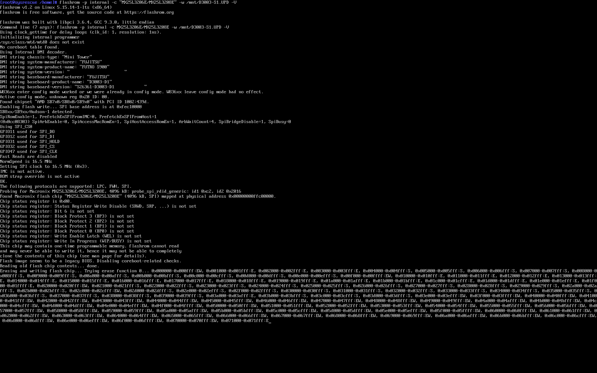
It went well:

This was the moment of truth: what happens after power-cycling the S900???
It actually worked!! See yourself:
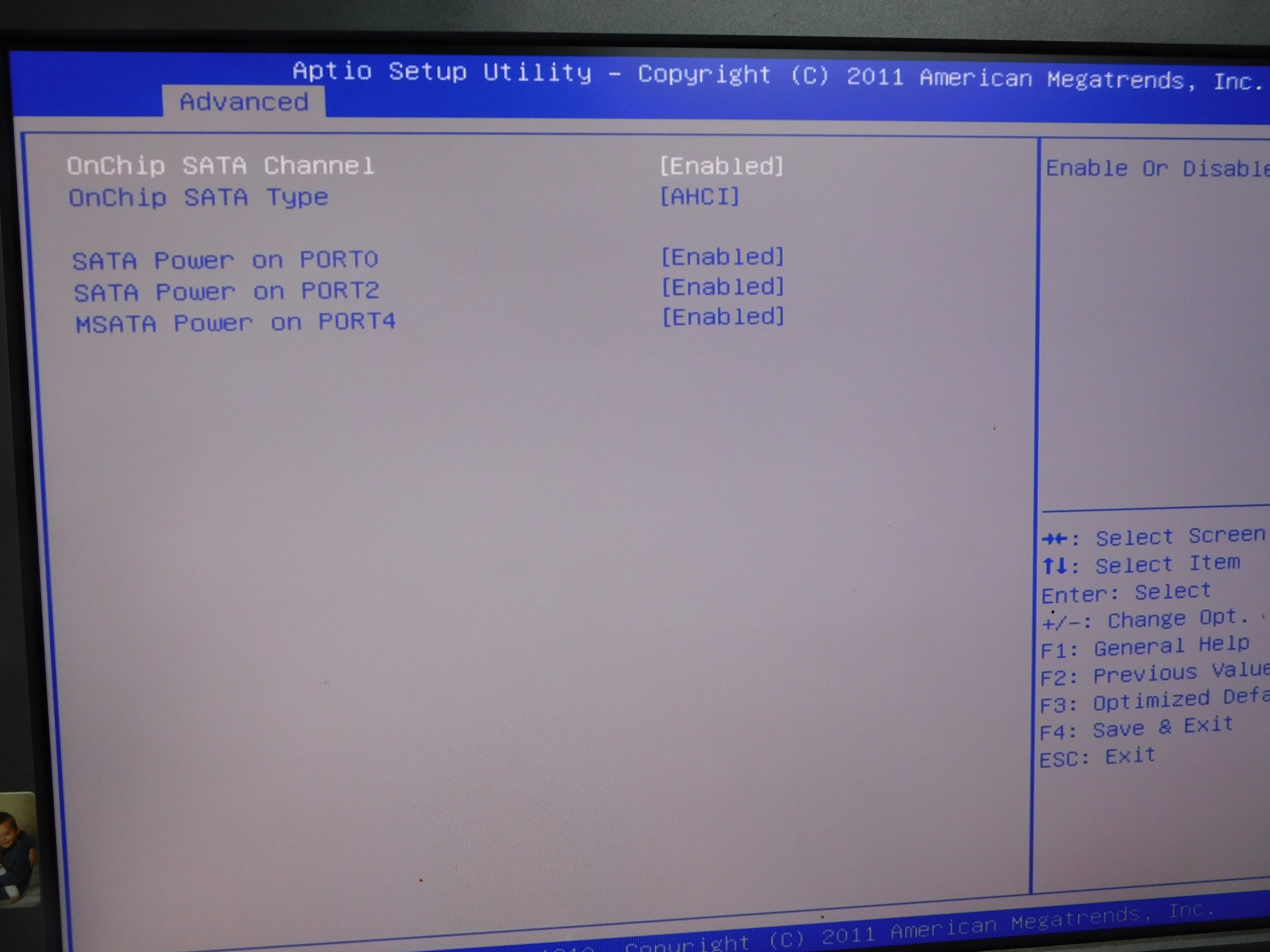
An additional SATA port 2 appeared. Mission accomplished!
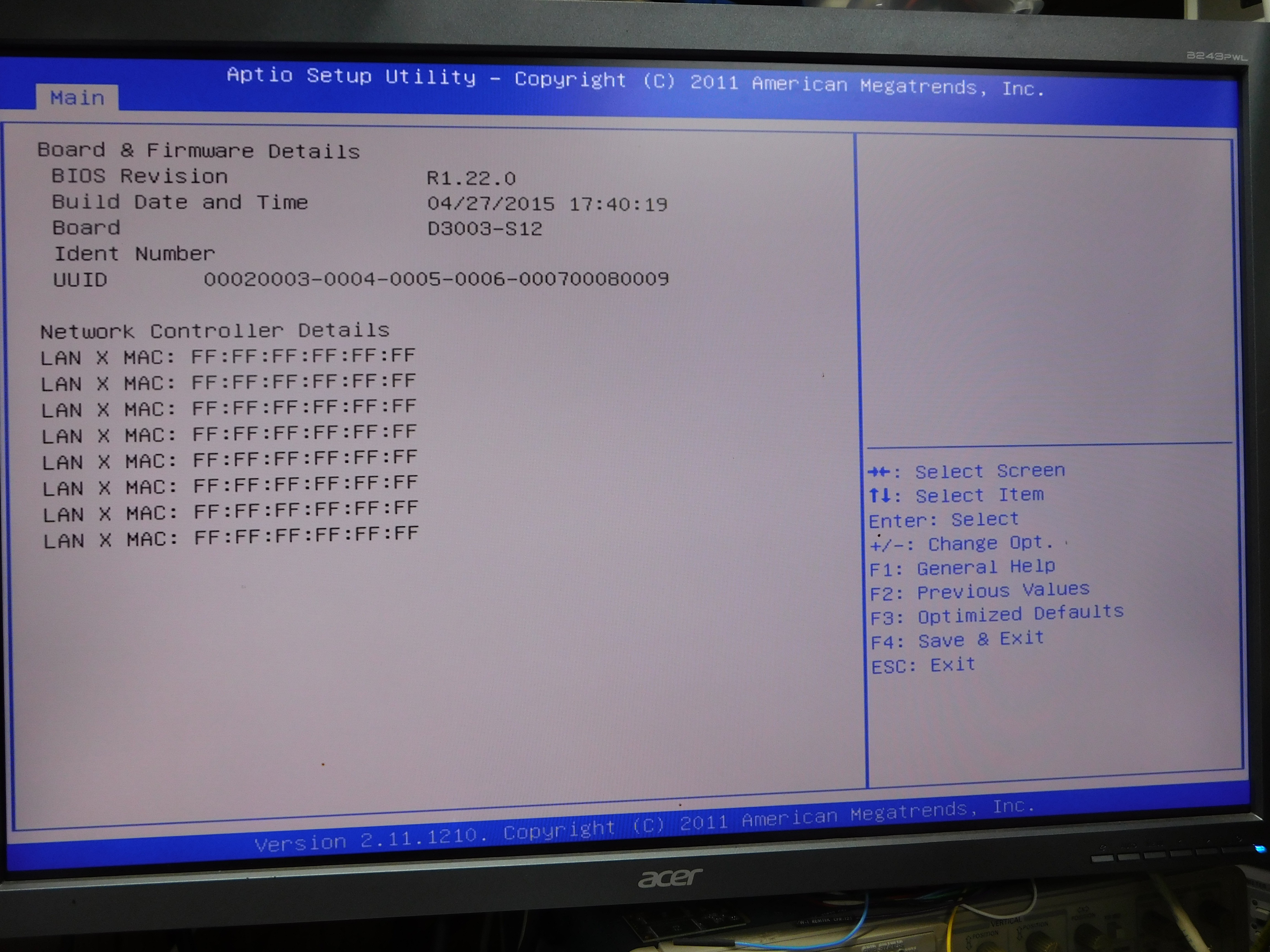
Some quirks remain. The poor brain-transplanted S900 is a bit confused about the number of LAN interfaces it was born with:
The...
Read more »


 Guido
Guido
 tomcircuit
 jimshortz
 Plasmode
@SK1 I did this a few days ago and it worked. The series capacitors should be around 10 nF (perhaps 15 would be okay too), size 0402 (1 mm x 0.5 mm). If you have some old PC motherboard laying around you can desolder them along with the connector (it takes a bit of practice not to melt the connector). Note that the connector is oriented the other way around than port 0, you can see it in the tech notes PDF.
As for the BIOS file search for "D3003-S1x - Admin package - Compressed Flash Files" on Fujitsu support website, download the file and extract "D3003-S1.rom" (or the D3003-S1.UPD file, it is exactly the same contents). No modifications to the file are needed - it is simply for a different variant of the same base motherboard.
EDIT: One more thing - on my S900 the BIOS chip was made by Spansion, not Macronix, so it required a different setting in the flashrom utility. It's not a big problem, flashrom can detect which chip is on your board.