[22:50]
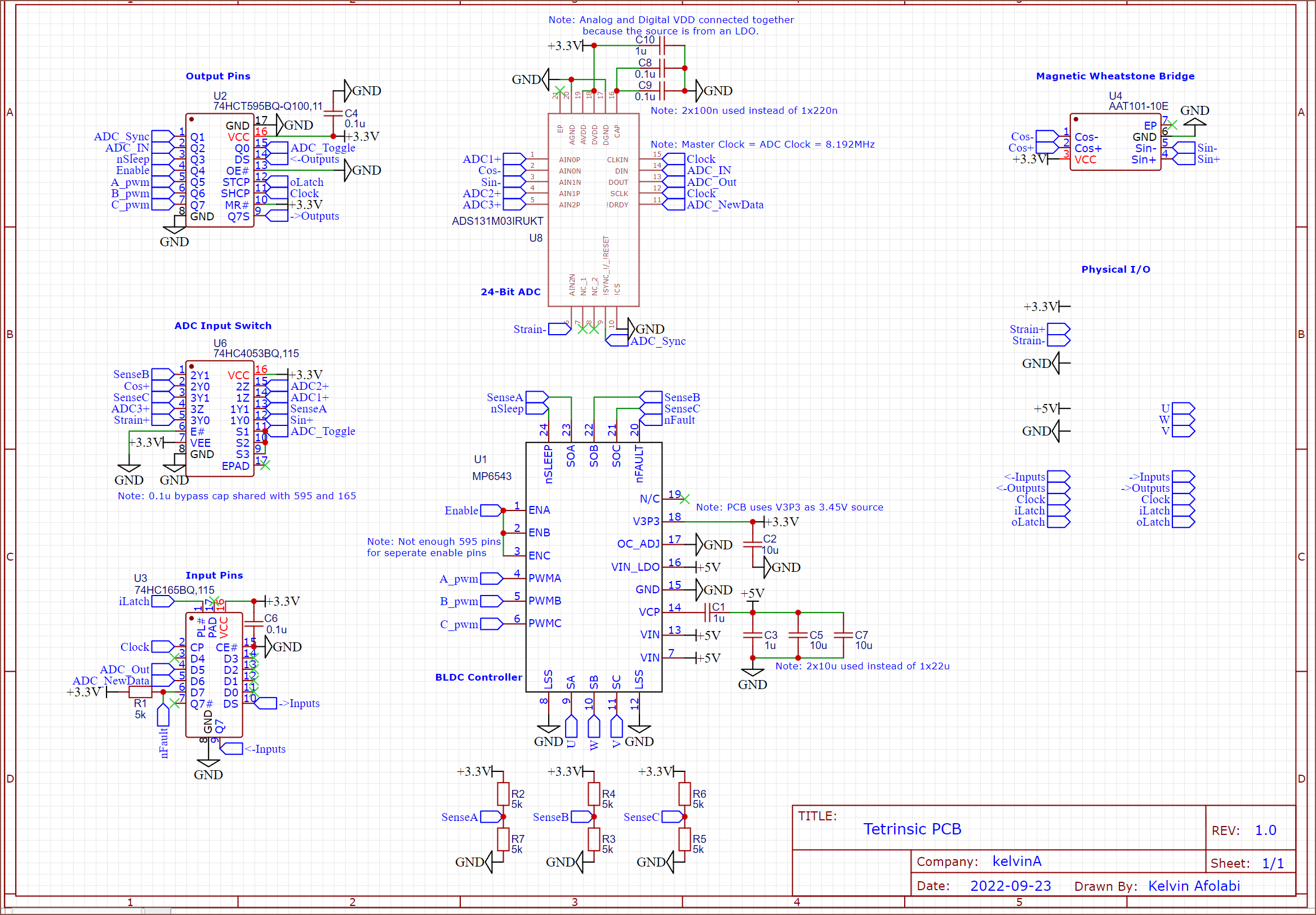 Ok. I've spent the past 2 days drawing up this schematic. The license is going to be under some permissive option but I've just been reading datasheets and connecting the dots so...
It's a good thing that I haven't just press "Buy Now" on anything yet because, as you can see, there are 6 chips and not 5 like in the previous model.
One thing I have learned is the "bypass capacitor" which is 0.1uF (and 1uF and 10uF) as a kind of industry standard. Another notable mention is that I'm going to see if I can get away with the analog and digital input voltages coming from the same source. It sounds like to get any usable-for-high-resolution analog source is going to require experimentation and osiliscopes, so I should just get any PCB out of the door now.
My chronological schematic creating process in detail is written below.
Magnet Angle Chip
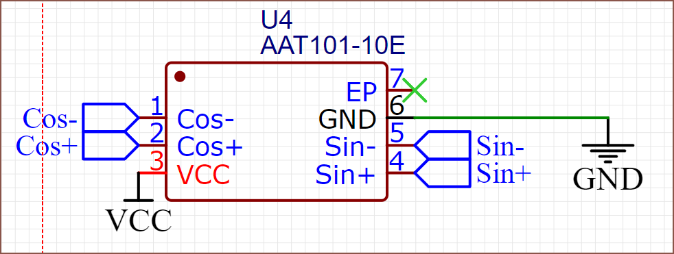 Ok that's 1 chip down.
 Motor Chip
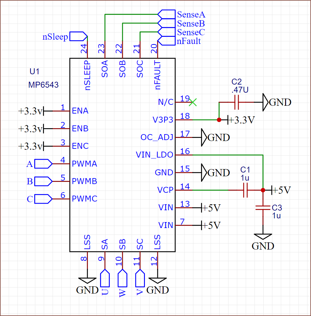 Is that everything? Wait a second... aren't those sense pins analog?
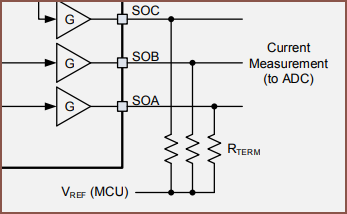 Nouh!! I'll come back to this later.
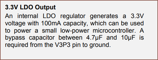
??? Didn’t you say 0.47 a moment ago?
 Hmm. Ok I'll assume the paragraph is the correct one. But nice! There's a 3.3V regulator in this chip, so I don't have to send that power from the MCU.
Switch Chip or new ADC?
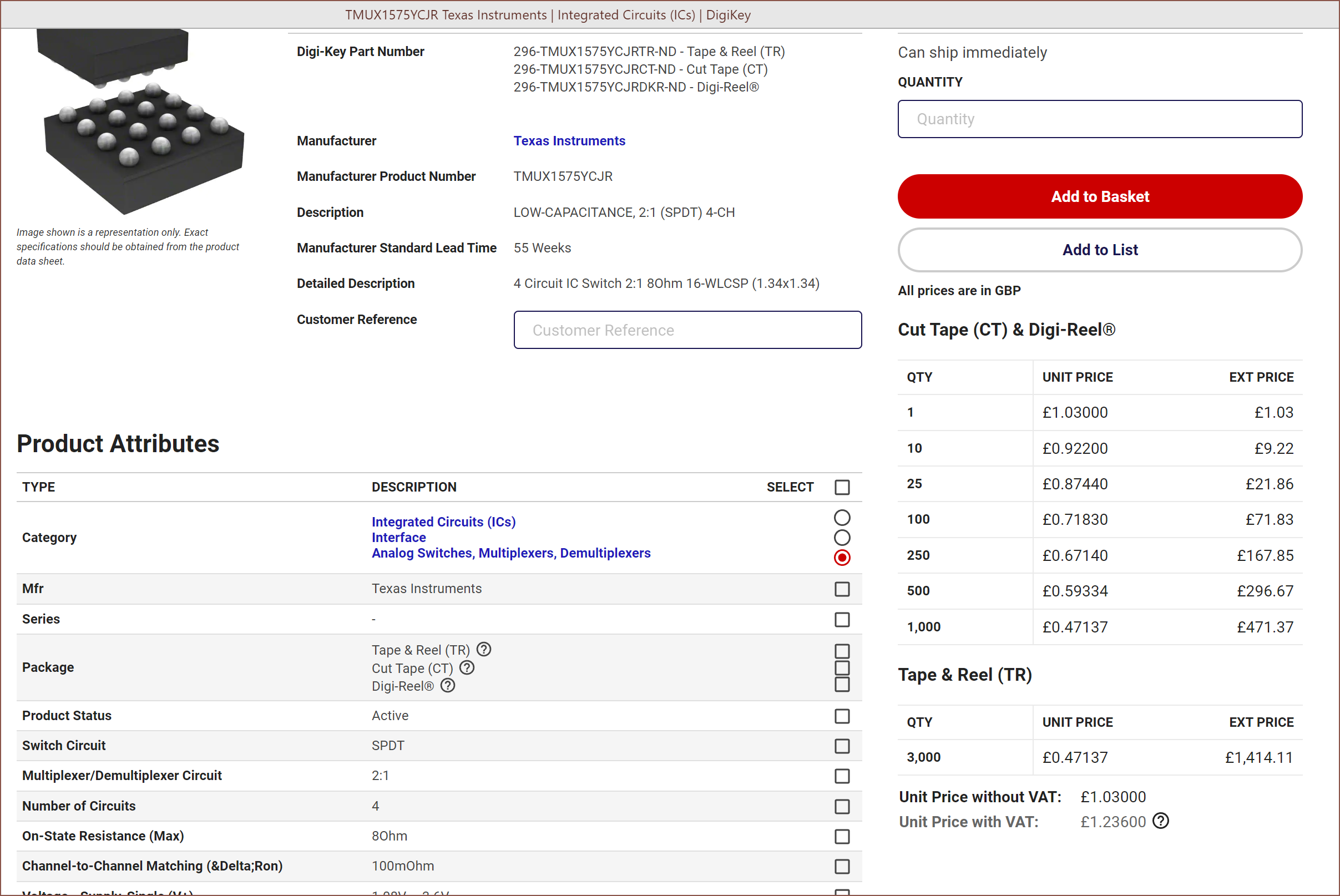
This sounds like the thing I'd need, but this is seemingly the only option that fits and is under £5 each. What I can do is use this in conjunction with the internal multiplexer of the ADC to switch between Signal+,Signal- and Sense,AGND:
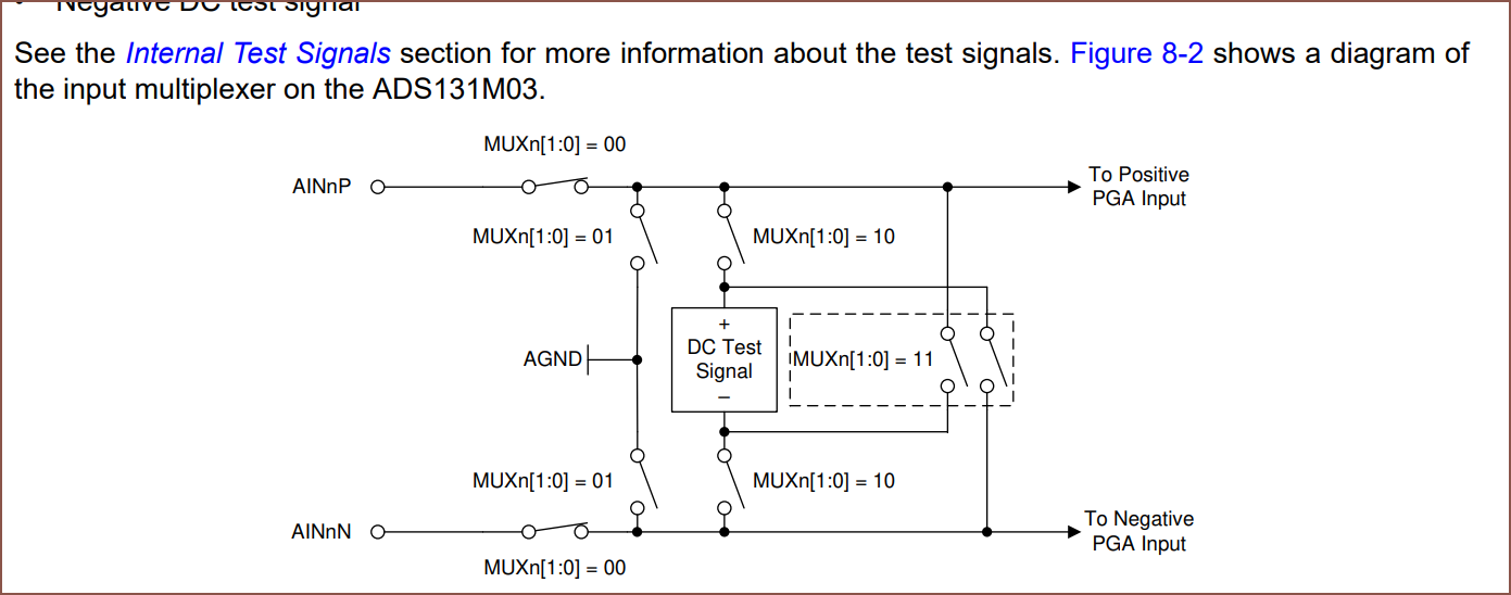
The issue is that I don't have a free pin on the 595 to controll the switch pin as of now. There's also the option of looking for a new chip. I've found the MCP3561:
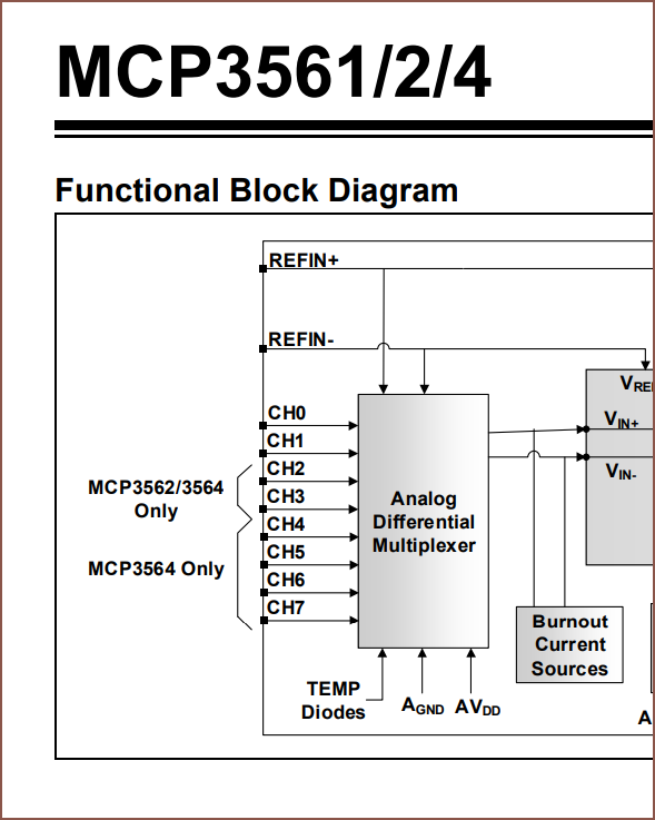
Here's my idea:
- Strain on channel 0 and 1
- Swap the aat101 for one of the single-pin versions (like 003)
- Sin on channel 2
- Cos on channel 3
- Sense on channel 4 - 6
 But that's the worst case option.
A second 595
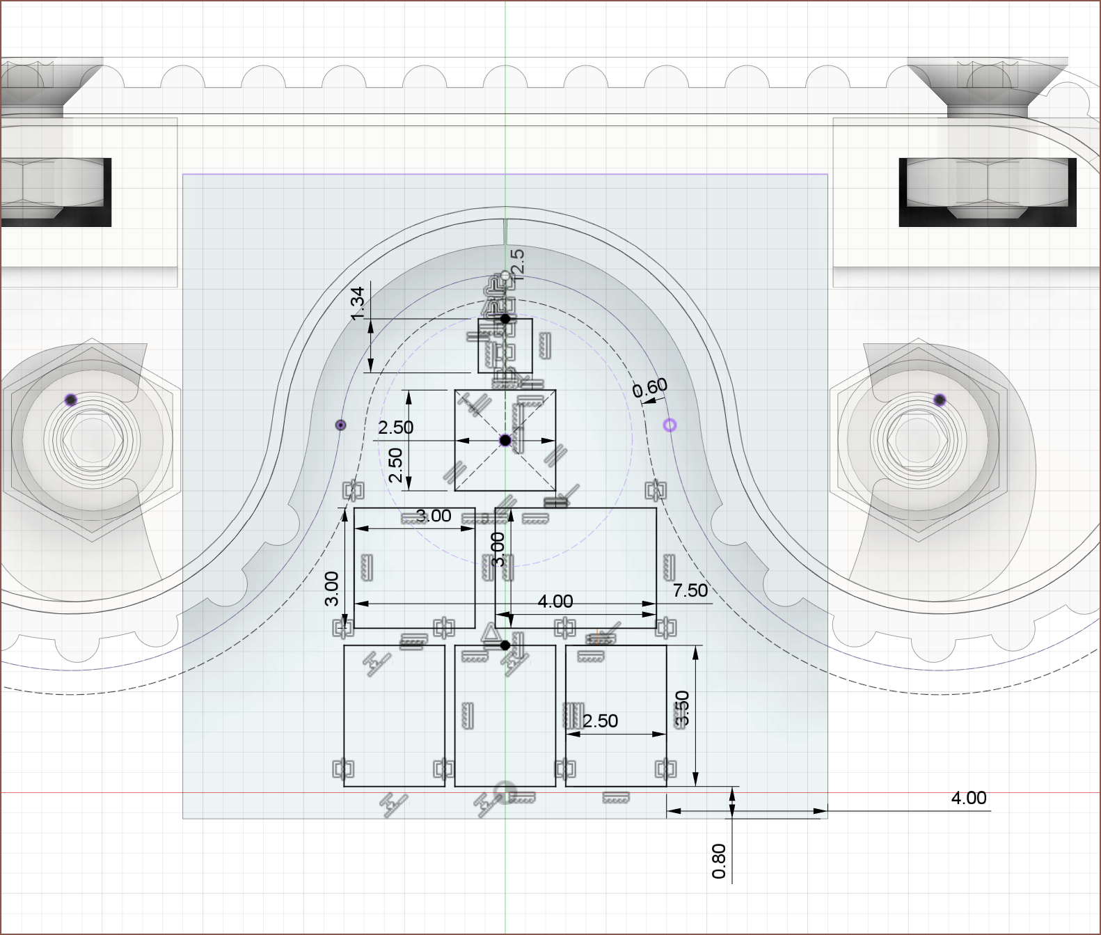 By increasing the PCB to 16x16mm, I could get this layout and also have plenty of output pins with the dual 595 chips. That ultrasmall 1.34 is also the only chip that would even fit in that space.
 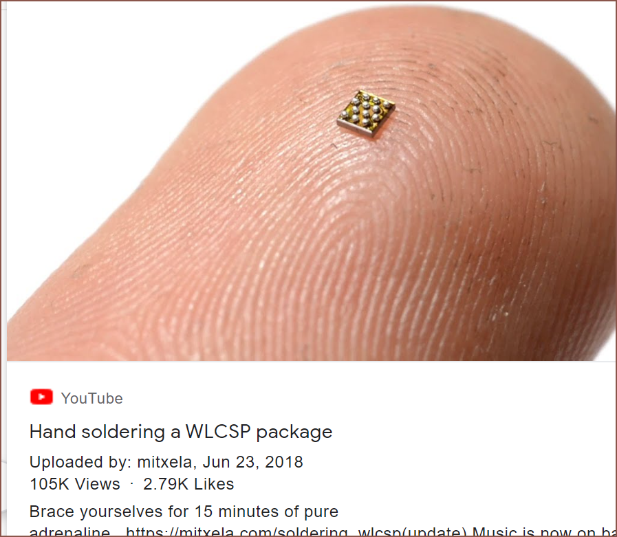 HAHAHAH. I'd probably have to buy spares with that kind of size.
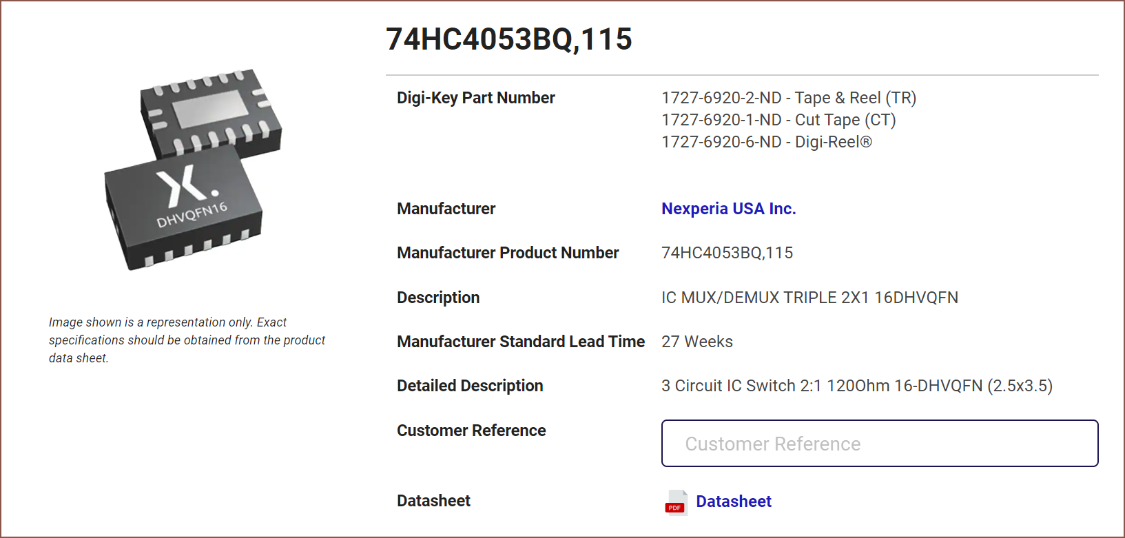 I found this, and it's half the cost as well as being the same sized package as the other chips like the 595. I'm kind of worried about the 120 ohm resistance, but I think the ADC has a much higher impedance anyway.
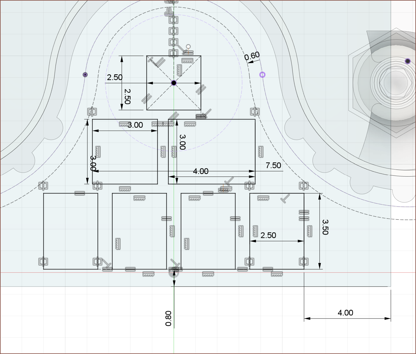 This is probably a much less riskier run, and I just had to increase the board width to 20mm.
ADC Effective Resolution
Reading datasheet of ADC...
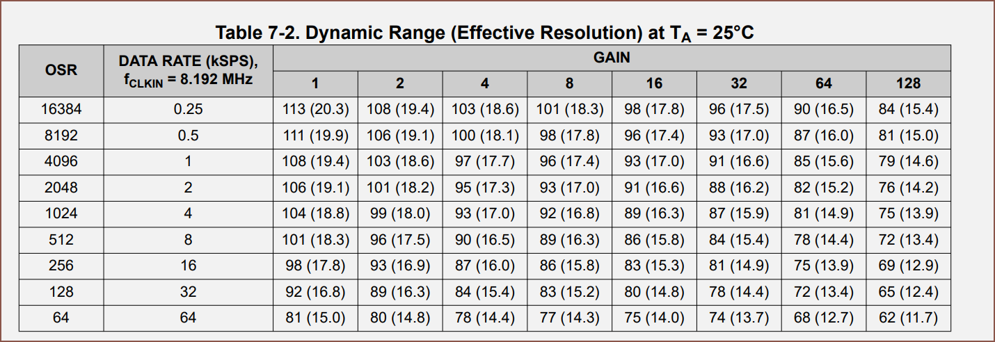
What's even the point of 24-bit if I'm not even hitting 16 when the noise is added in?
Adds/Removes components needed for the 8 channel, 16-bit ADC.
Price is £132.49 for the current ADC and £139.78 for the proposed new ADC.
But wait. I've got 7 channels I need to scan through and there's only 1 ADC doing the work. That's
153600/7 = 21942 samples per second.
(Before starting on the schematic, I got some button press numbers. The fastest I could actuate a keyboard press was 0.08 seconds. The last thing I want to happen is that my speed-increasing input device isn't fast enough to keep up. Lets say I want 1000 samples for keypresses for high precision and low latency. That works out to a minimum of 12.5ksps. At this moment, I don't know if I need more or can get away with less samples, so I set that as the target)
Returning to the ADC, this means I can only use the 32 OverSampling Rate option as 64 would mean I get less samples than the target. Thus, I'd only get 12.6-12.8 bits of data (with the remaining 3ish being noise I assume?).

Meanwhile, on the current ADC, I can do 32K samples at 128 OSR and get these numbers (1,2,4,8,16 gain)

There's no 16 bit variant of this current ADC though, which might've saved some money.
The Clock Signal
I just realised that:
- I've got a free pin now that I don’t need to send 3.3v.
- I can't send the clock pin for the bit shifters via the bit shifters.
I might be able to go back to one 595.
More ADC work
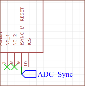
What am I even supposed to do with this? Isn't this to connect to OTHER chips and not the MCU?
 uhhhh... CAN'T I USE THE CLOCK??? I think I'm gonna risk it and go down to 1 595--
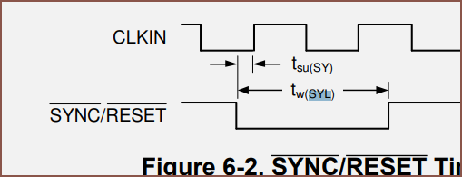 No I can't; the time period is too long.
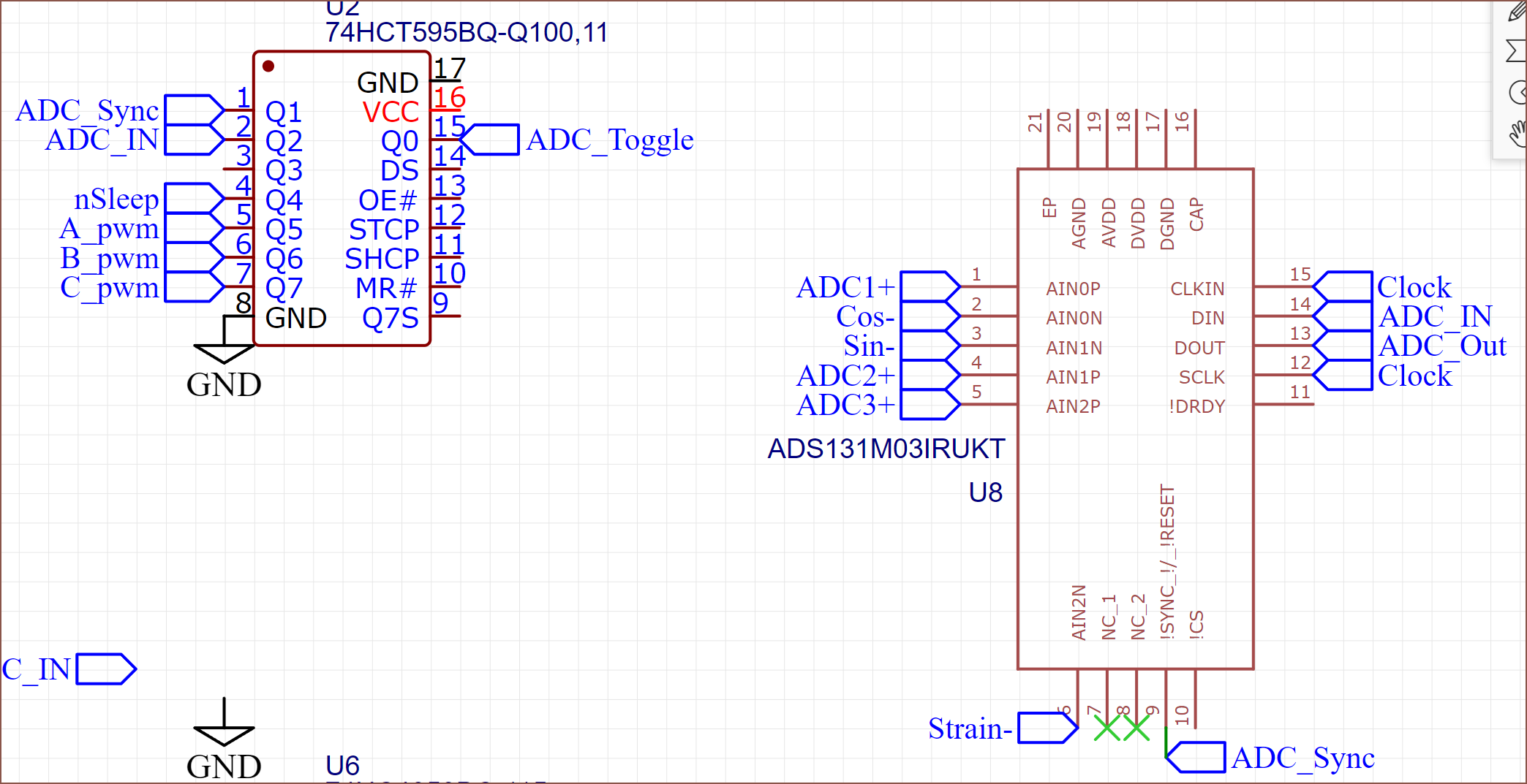 Do I even need a chip select pin? Reads relevant part of datasheet. No I don't, because the 595/165 means that it's as if each chip now has it's own MOSI and MISO line instead of sharing.
The 74HC595 and 165
I read some Arduino docs and other sources and found out that if I connect both register clock pins to the same clock, what will happen is that the output pin signals would just cascade down the chain. I don't want that. This means that I need to add a "Latch" line to the ribbon cables.
Additionally, it seems that the 165 can't share this latch pin since it'll result in undesirable behaviour. Thus, a 5P cable would be needed.
I also found out that "I/O Expanders" exist which can do input and output, but to get one that works at the 8.192MHz used for the 24-bit ADC, it's going to add another £2.68/each (minus about 90p by removing the 595/165) to the BOM for a 16 pin chip. That'll be nice though since I've only used less than half the available input pins on the 165, but I could use more output pins.
Just go with 20mm wide.
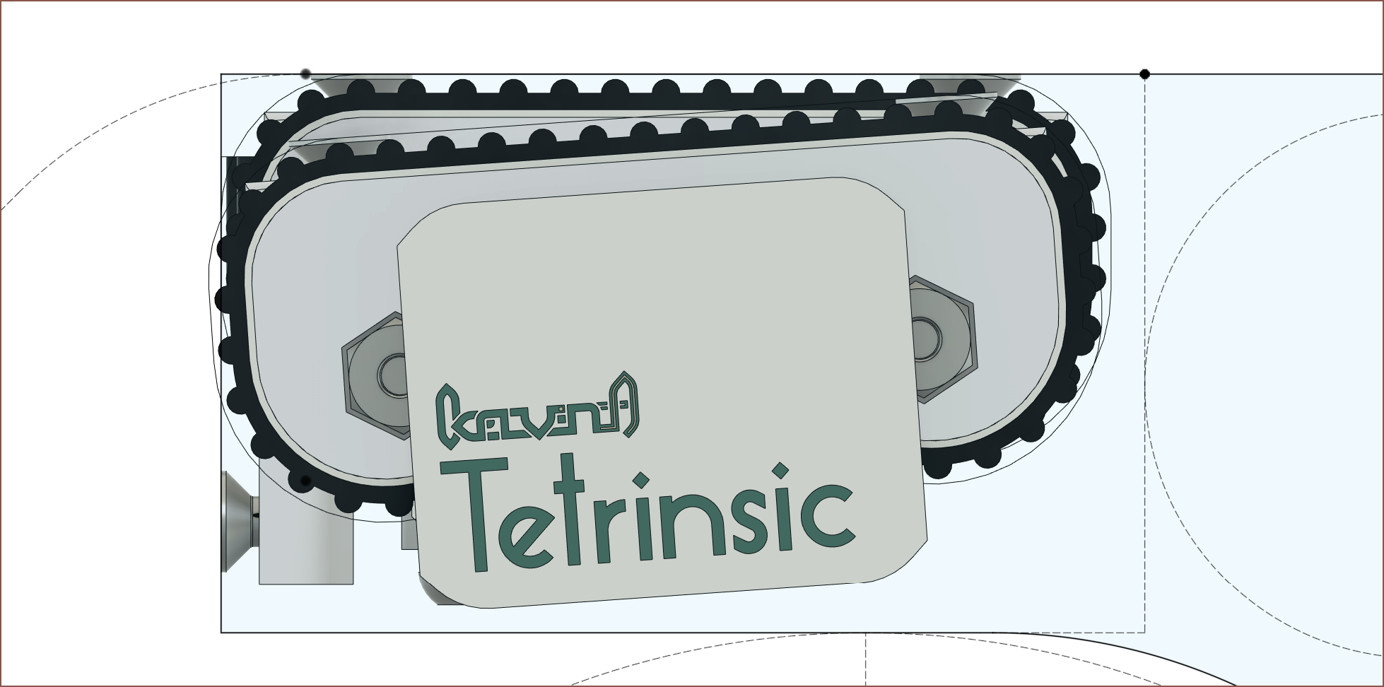 I really should just make the board wider to accomodate for wider ribbon cables. It doesn't even make that much of a size difference for this currently-untested 4 degree slope (for Finger4 on #Tetent Timespy [gd0136]).
And to end off Day 1, finishing the 165 part of the schematic:
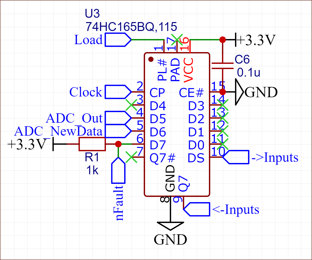 I don't know what to call this second latch pin so I've named it "Load".
Day 2 started with me wondering if there was a board that used the MP6543
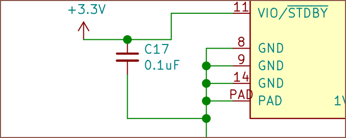
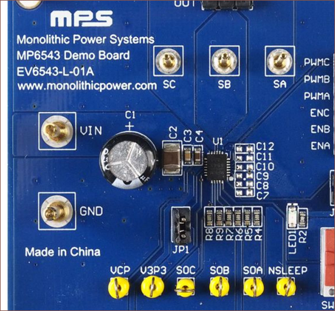 Oh, there is. What MASSIVE capacitor is that though?? I was wondering why the 5V capacitor was never specified. Is it like the large one used for stepper drivers?
 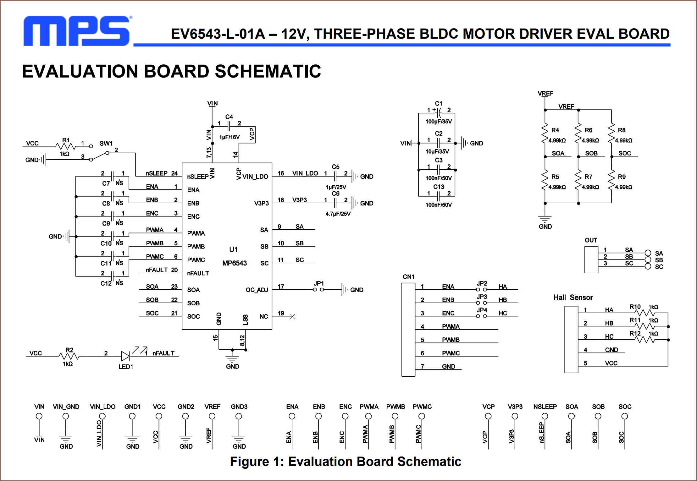 Ah, a schematic. It's a 100u, 35V capacitor? And I assume the other 3 are for something analog-smoothing related? I don't remember something large like that on the SmartKnob View. It's a shame I could only find an interactive BOM and not the schematic. Anyway, it seems that:
- .47u was indeed a mistake for V3.3.
- I guessed correctly that V-in uses a 1u cap. I assumed it was the same as the V-in-LDO, which specified a 1u cap with at least 10V tolerance.
- V-in-LDO uses a 25V cap instead of a 16V. Interesting.
- I didn't expect that the V-ref stuff was supposed to be a voltage divider.
Google: smartknob view schematic
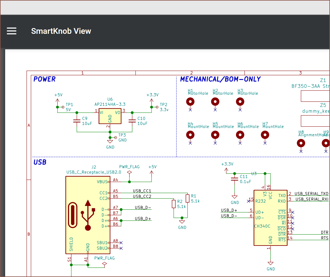
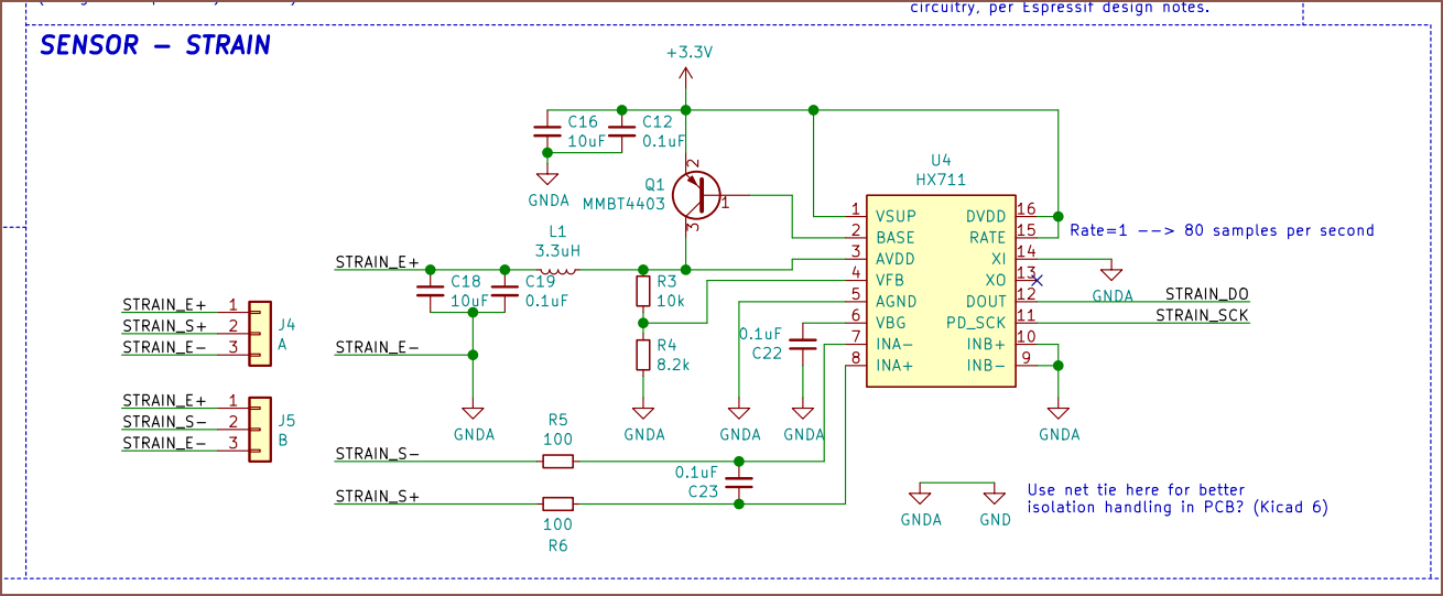
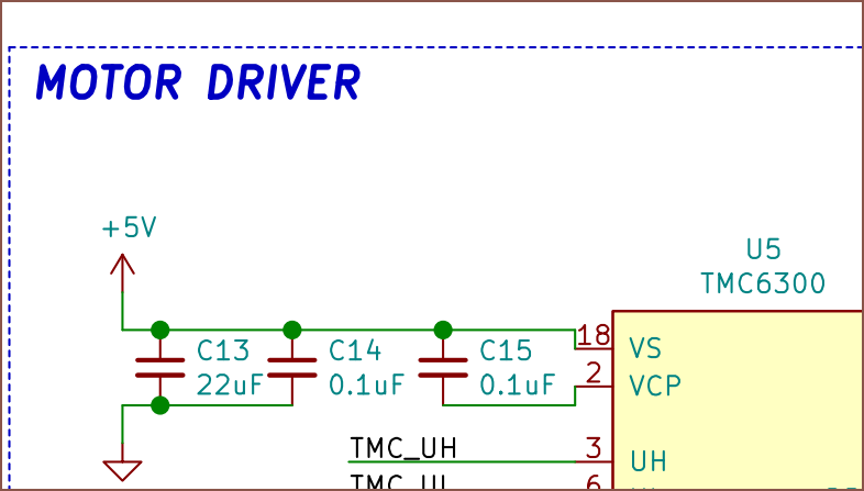
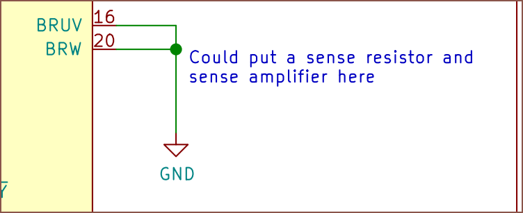
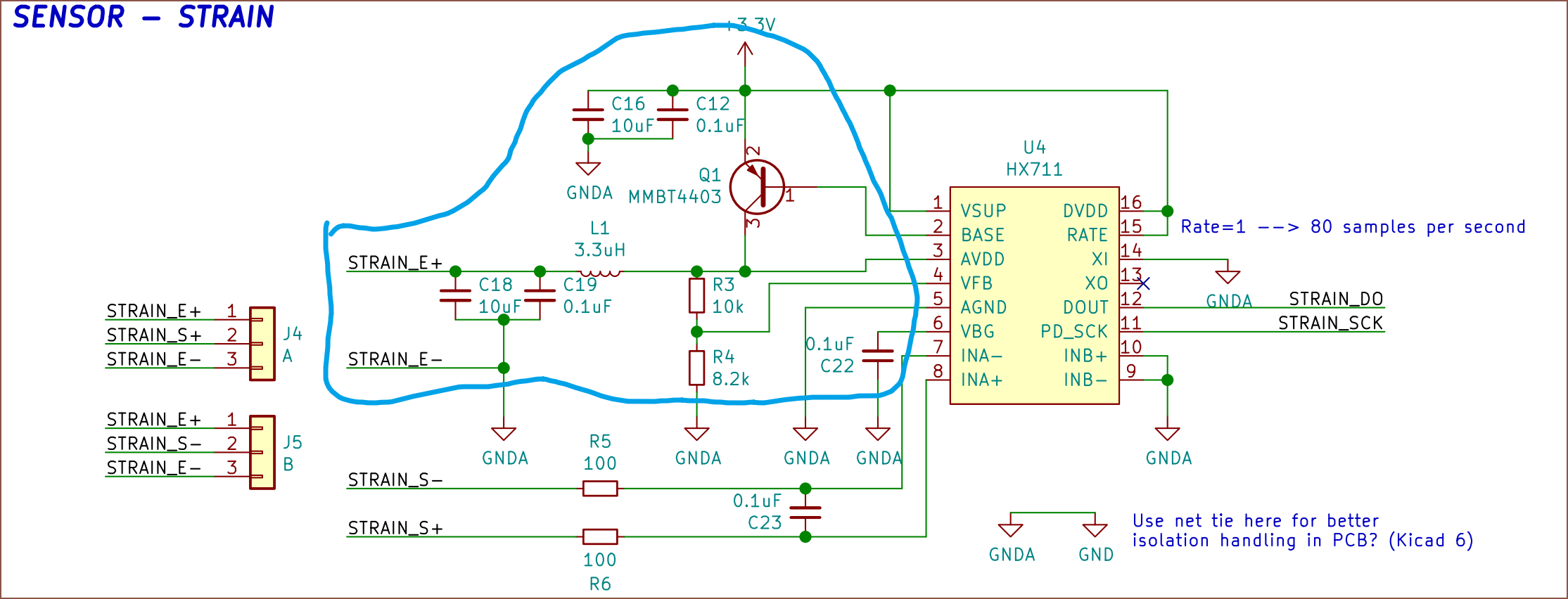
YOU DON'T SENSE ANYTHING?!!?! How though??? I thought you needed both current and rotor position for Field Orientation Control! Well I've already done all the work and the extra chip is like 40p/each so I'm not going to rip it out now. It just means that I can take more samples of the main analog things and less samples for the motor currents.
More MP6543 motor controller work
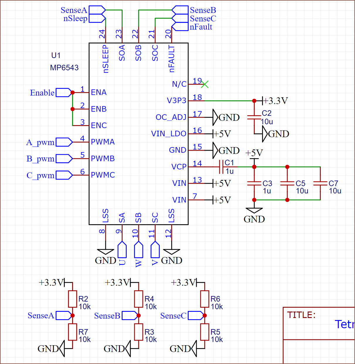
Ok is this better? I don't want to have to source multiple capacitor values, so I've done:
- 4.7u ->10u (max allowed in datasheet)
- 22u -> 2x10u for a total of 20u
- I'm also going to change all resistors to 5K. This includes the nFault pull-up resistor I think I need.
I wonder if there's a similar demo board for the ADC?
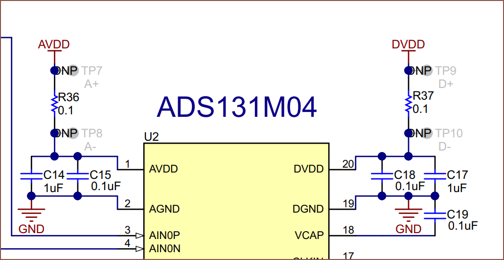
Even more capacitors?? These bypass caps are everywhere. Oh, and how am I doing AVDD?

Does this mean I could use the LDO from the MP6543? I'll try it. Right now, I'm a bit more concerned on how I'm going to fit everything with only 2 traces (and 0 ohm resistors) to work with. JLC's price goes up a lot if I ask for 4 layers.
And that's how I got the current schematic.
I've likely missed a few considerations here and there, but I think this log is a bit more useful than "I spun this schematic up over the last 24 hours.".
I do think the solution I've got is more versatile than if I only made a PCB with an angle encoder on it, since now someone could easily make a non-split, 8 Tetrinsic keyboard by soldering a daisy chained collection to 5 pins on the MCU, or it could be integrated into more traditional keyboard designs as the pin count cost is low. The alternative would've been to add all the other components on a single PCB that the MCU is soldered onto.
I'd also like to mention that it feels like I'm playing 2048 a bit.
- #TetInventory [gd0039] can't really be designed because I don't quite know what additional things I need in a backpack along with Teti (cables? table clamps? wrist rests?).
- #Teti [gd0022] progress has been stalled because Tetent can -- and has -- influence(d) design tweaks, as well as the lack of CR600S (see #Printer Repair [gd0137]).
- #Tetent [gd0090] can't exist at the moment because there's no such thing as a "motorised slide encoder", let alone one small enough to be used as a keyboard switch replacement or pressure sensitive.
- Tetrinsic hardware seems viable, but I won't know yet because there's no small PCB I can just add to my AliExpress cart.
- So now I'm here, creating a daisy-chainable, pressure sensing, BLDC encoder + controller on 20x16mm of board space.
- Hm. So then it's a miniaturised SmartKnob non-View, designed for a different use case?
 kelvinA
Discussions
Become a Hackaday.io Member
Create an account to leave a comment. Already have an account? Log In.