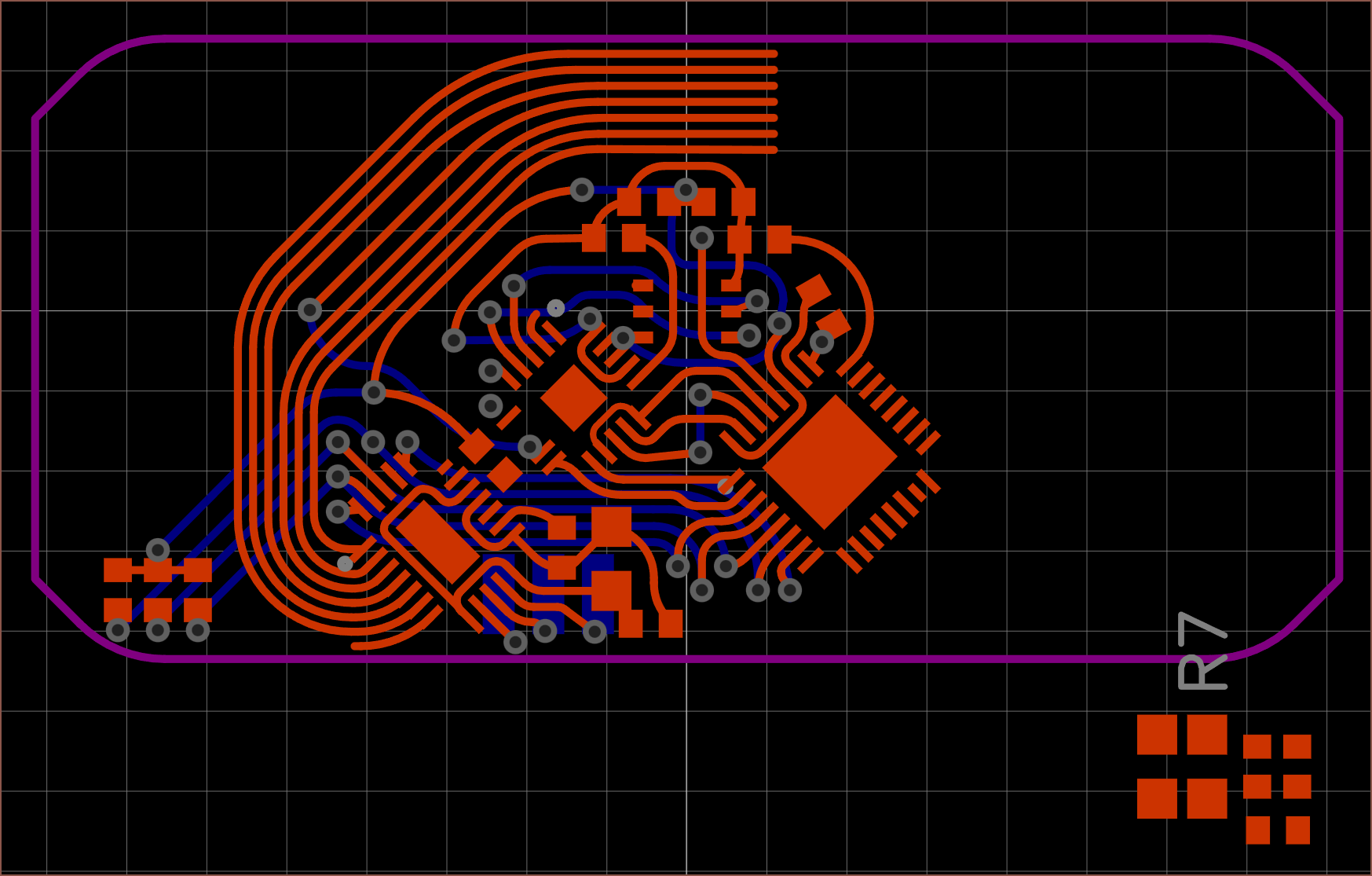
 I've sunk 5hrs into the next PCB iteration. The challenge is, as usual, to have everything connect up. I'm also routing the ground pins now. Connecting the ADC to the microcontroller and angle sensor was straightforward, but its the MP6543 motor controller that has increased the compute time. I have also checked Digikey to see if there are any new alternatives in stock that wasn't a month ago, but there were none. I'm using the LDO that's conviniently on the MP6543 so it's not like I can switch to the now-in-stock TMC6300.
I've decided to put solder pads for ribbon cables on the back side of the PCB to get more space on the front and ease assembly, and I think it was a good idea to go with.
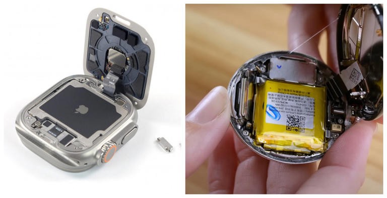
I've also recently seen the below image and even though this is the first Tetrinsic board design, I'd still like it to look nice for my inner peace of mind.

 kelvinA
Discussions
Become a Hackaday.io Member
Create an account to leave a comment. Already have an account? Log In.