Nate Rivard
-
Part 5: Finite State Machine
10/21/2024 at 12:17 • 0 commentsOverview
It's time to design the subsystem that ties the whole device together: the FSM (finite state machine). The FSM for SPI Master will control the data register's communication with peripherals: starting, stopping, and sychronizing the shifts between orchestrator and peripheral. We can define our FSM very informally:

When the RUNNING signal isn't asserted, we're idle. When RUNNING is asserted, we move to the shifting phase. We shift 8 times on the positive edge of SCLK after which TX_COMPLETE is asserted and we move back to idle. We'll go into more detail in the design section.
Design Considerations
Here are the constraints our FSM must conform to:
- it can be moved to the RUNNING state
- it signals to the data register to shift exactly 8 times
- it signals that transmission is complete and returns to idle state
Design
The first part of our design is reasonably straightforward: we need to be able to set and unset a running state. In chapter 1 designing the control register, I said we'd address the unused half of our 74HC74 in a later post. It's time to put this piece to use.
The idea is pretty simple here: when a write is done to the data register, RUNNING will get set. When transfer is complete, RUNNING will get reset. In this design, we are not qualifying setting or resetting with the clock, we are taking advantage of the asynchronous pins of the register. Will this come back to haunt us?
Before we can discuss the next part of the design, we need to dig into more detail on SPI as a protocol. In the project overview, we said this device was only going to support CPOL = 0 and CPHA = 0. What does this mean?
CPOL, Clock POLarity, describes what state the clock is in when idle. When CPOL is 0, clock will idle low. CPHA, Clock PHAse, describes when values are shifted and when values are sampled. When CPHA is 0, it means values are sampled on the positive edge of SCLK and values are shifted on the negative edge. To help illustrate this, here is some SPI traffic captured between an AVR and an SD card:
You can see at the bottom, SCLK idles on zero. It's hard to tell when values are sampled here but it can be seen that bit values are prepared on the negative edge. It can also be seen that bits are transferred in chunks of 8, a byte.
Now we can design the timing module. To start, we need a way to count to 8 and we need this to be final on the negative edge. In a previous chapter, we used a 74HC393 to divide the clock by powers of 2, but we can also use one to count up, that's it's primary function! When simulating it appears like we get what we want:
When cleared, after 8 clock cycles, we assert a transfer complete signal. So far so good. But what about when the device is first powered on? What about when the transfer is complete? There is no real CLR logic here. The original design looked like:
I'm not going to discuss this much because it's not the final design, but the idea was that either asserting /RES (active-low) or asserting TX_COMPLETE would reset the device.
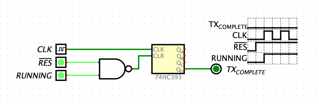
One major problem with this, though, is that TX_COMPLETE is a one-time event. But go back to our FSM diagram. The diagram there shows /RUNNING as a valid (and let's say potentially continuous) state. As long as we're not running, we shouldn't be counting. We also already establish storage for RUNNING, so let's use that instead:
This is looking closer now. There's another major problem, however. Recall that values are sampled on a positive edge, and prepared on a negative edge. This means that our first bit actually needs to be prepared and valid before the first positive edge. This creates a complex and perhaps hard to predict race condition. Consider:
- RUNNING is set on a write of the data register
- the '165 shift register in the data register immediately puts the MSB of its contents on the serial output line
- the '393 immediately starts counting when RUNNING is set
In this model, we are trusting that the '165 will always puts its contents out before the first negative ('393 is clocked on the negative edge!) edge of the '393's clock. It might be a valid assumption, it might not, but it's difficult to model and test. So is there a better way?
There is but it comes with a cost. This idea (but not exact implementation) was inspired by the CPLD code from Daryl Rictor's 65SPIv2. For that project, he uses a 17 state FSM: Idle and 16 clocks. In this sense, we have currently attempted a 9 state FSM: Idle and 8 clocks. Let's change to a 17 state FSM and see why might it be better.
The first change we'll do is to make the SPI clock a product of the state machine, not an input! In the above design, the FSM takes the SPI clock in as an input as does the data register. This can create those race conditions we just talked about. By shifting the responsibility of generating the SPI clock to the FSM, we can have more control over it. This comes at the cost of the SPI clock being at best half the speed (depends on which tap from the '393 we use) of the incoming clock. We can make a change to our clock select module later to address this.
The second change we'll make is to use both counters in a '393 to get to 16 states. One counter in a '393 only counts to 15 then resets to zero, but we need to know when it rolls over to differentiate between reset/idle state and completed state. This comes at the cost of a 2nd '393 chip in the overall design (we still need one counter for our clock select circuit.)
We can see a simulation of the new design:
Here, when RUNNING and CLK are being asserted at the same time, the SPI clock doesn't happen until the negative edge of the first clock. This gives the '165 plenty of time to assert the first bit on its output before the SPI clock goes positive. As counterpoint, here's the old design when RUNNING and CLK are asserted at the same time:
In this design, the '165 shares the clock with the FSM so we can't be sure what went out.
These simulations have exposed another flaw in our data register. Recall that the next bit to be shifted is supposed to prepared on the next negative edge. Currently, the '165 is shifting on the positive edge of the clock! The simple fix here is to negate the SPI clock for the '165:
This takes advantage of the fact that the '165 only shifts on a negative edge as opposed to level. If it shifted on level, it would shift while idle because CPOL = 0. Instead, we see:
- CLK is low while idle but is negated so appears as a high level to the '165 (no shift)
- '165 is loaded with data and QH reflects MSB on load (no shift)
- CLK goes high causing the '165 to see a negative edge (no shift). Meanwhile, the peripheral just sampled QH because saw a positive edge on the SPI clock
- CLK goes low causing a positive edge when negated to the '165 (yes shift!)
And so on each period of the SPI clock, this design has the proper bit prepared for the positive edge, and shifts to the next bit on the negative edge of the clock. The FSM has complete control of the clock and stopping the shifting sequence.
There are more issues with our data register but at least the FSM is done.
-
A Note on Tooling
10/17/2024 at 16:52 • 0 commentsTools
As I said in the project update, I couldn't get my initial design to work. I have an oscilloscope and a very cheap logic analyzer but using these tools is cumbersome and finicky. They can only measure what goes to the pins, not what's happening internally. Strict timing control is hard to do and measure. Moving physical devices and wiring around is time consuming and has the potential to introduce new bugs each time you do it.
What I needed was a way to see signals at the gate level, a way to synchronize signals, and a way to quickly swap gates in and out without moving a bunch of wires. So I moved to software.
Digital
For now, I am very much enjoying the interactive nature of Digital, an open source logic circuit simulator by H. Neemann. With it, I can start to slowly build out my circuit, play with it, and see what happens.
Out of the box, Digital also has a number of simulated TTL circuits!
Here you can see both the '165 and the '595 from the data register. It doesn't, however, have everything. Some devices, like the '393, are missing. What to do?
If You Build It, They Will Come
Digital lets you model things at the gate level, so let's add a '393 to our library. Where do we start? With the datasheet, of course! Many (maybe even most?) datasheets include a logic diagram that gives you the function of the chip. Here's the logic diagram for the '393:
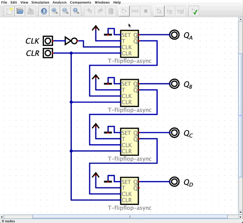
Here you can see the signals and basic parts for a single counter (there are 2 in the package): an active-high CLR, a clock on the negative edge, and 4 T (toggle) flip-flops. Let's use Digital to recreate this circuit. We'll start with 4 T flip-flops and a clock:
Digital has built in T flip-flops. This is hooked up like it appears in the datasheet, but what about T? In a T flip-flop, T acts like an enable signal. When high, toggling is enabled and when low toggling is disabled. The '393 has no enable/disable signal so we'll tie this high. Now let's simulate this:
That doesn't look right, it looks like it's counting down not up! And that's because when you toggle the clock, Qa goes high, which is the clock for Qb so it goes high, which is the clock for Qc, etc. How do we fix this? By using the inverted outputs as the clock for the next stage:
There are still 2 problems here, though. The first is easy to fix: the '393 clocks on the negative edge, while this circuit is clocking on the positive edge. Simply inverting the clock signal will give us the desired result.
The 2nd problem is tougher. When this circuit starts up, you can see random values on all the outputs. Toggling the clock counts up but not from zero. We need the ability to reset all the flip-flops.
Unfortunately, Digital does not have a set/resettable T flip-flop. That's ok, though, we can make our own. Digital does have a built-in D flip-flop with set/reset. So we'll use this and convert it to a T flip-flop:
Next, we'll replace the built-in T flip-flops with our resettable T flip-flop, hook up the CLR line, and correct our clock:
And there you have it! We now have a functioning '393 to use in a larger circuit.
But why go to all this trouble? To validate the SPI Master, I previously used a built-in binary counter, but its characteristics were not like the '393 (positive clock edge, synchronous clear, etc.) It's important to simulate actual hardware as closely as possible when translating to the real world.
-
Part 4: Data Register
10/16/2024 at 09:28 • 0 commentsOverview
The next design we will look at is the data register. This subsystem is the piece that actually interfaces with the SPI devices. It is responsible for both sending 8 bits to and receiving 8 bits back from a peripheral, 1 bit at a time (remember, SPI is a serial protocol!)
Design Considerations
Here are the constraints our data register must conform to (many of which are the same as the control register!):
- it needs to fit in well in a 6502 memory-mapped environment
- it must be safe to read and write
- it must be resettable
- it shifts 1 bit out, MSB (most significant bit) first, on each SPI_CLK positive-edge
- it shifts 1 bit in, MSB first, on each SPI_CLK positive-edge
Design
SPI is a serial protocol but the interface to our microcomputer is parallel, so we need to choose parts that can translate between the two. This is the core of the entire device so we need to get this right!
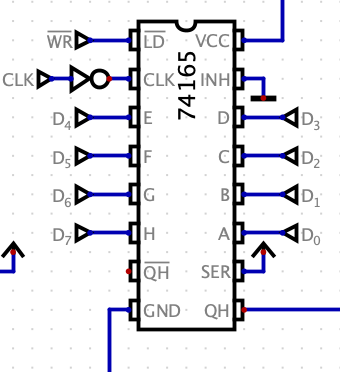
We stated in the project overview that transmission will start when a value is written to the data register, so we'll begin there. For this task, we'll use a 74HC165 8-bit parallel-in/serial out shift register. This shift register supports asynchronous parallel load (will be important later...) and shifts the MSB out on a clock pulse. This chip also has an "inhibit" pin which can be better described as /SHIFT_EN (LOW asserts that shifts are enabled and HIGH inhibits any shifting). So our design for the write side of the data register looks like:
We are using a special clock here, not the main clock and not the divided clock, because we're only supposed to shift 8 bits and then stop which will be covered by another subsystem. Shifting is also inhibited while writing to the register.
Next, we need to be able to read the byte received back from the peripheral. For this, we'll use a 74HC595 serial-in/parallel-out shift register. This shift register takes data in one bit at a time, MSB first, but can output the whole byte when /OE is asserted.
One major quirk of this device is that shifting and saving are 2 separate operations. There are actually 2 registers in this device: SR (the actual shift register) and R (the "register" I guess?) which is the register whose contents are put on the Q lines when /OE is asserted. If we forget to assert /RCLK at the end of our shifting, we will simply see the old contents of the R register, rather than our new shifted in bits.
I also have a pull-up resistor on the MISO line but most devices should already have this so it may not be strictly necessary.
Putting it all together, we get the full design:
Blast From the Past
So, does it work? Sadly, no.
First, we are going to drop one of the design considerations for the data register. We previously stated that this should be resettable. This should be simple, there is a /RES line connected to an active-low /SRCLR pin. Easy! Actually, no. Remember that design quirk from earlier? It turns out asserting this line only resets the shift register and not the register register! Additional logic is needed to assert the RCLK line on reset. Instead, I've decided to drop this requirement because contents of this register do not drive anything else in the device. If users want to read the garbage it boots up with, there is no harm in it.
There are a few other subtle mistakes here that will only become apparent when we examine the next subsystem, the beating heart of SPI Master: the Finite State Machine!
-
Project Update
09/19/2022 at 14:11 • 0 commentsProject Update
Is this project dead? No! It just didn't work and I got distracted. I designed and built a full Motorola 68000 based single board computer, a TMS9118 video card, OPL3 sound card, and wrote a lot of retro software. But this project has still been percolating.
What's Changed?
I breadboarded the project as outlined so far but it didn't work. Rooting out bugs purely in hardware is tough tough work because you can't see the interactions inside the chips and specialized equipment to view and generate all the signals (logic analyzer, oscilloscopes, function generators, etc.) is cumbersome and expensive. So I took a step back and decided to try to simulate the circuit in software first, iron out the kinks, and then lay it down on the breadboard.
I also looked at some other similar projects, namely Daryl Rictor's excellent 65SPI, a CPLD based SPI controller. His aims are/were very similar to mine: a clean interface to SPI for microcomputers. His working design includes the CPLD code which was an inspiration for some of the changes in my discrete design.
What's Next?
I have actively picked this project back up and hope to publish new logs outlining my progress. The current status is I have changed the design and simulated "working" hardware (this is actually tough to do even with current software tools). New logs will include both the original hardware design(s) for the pieces, failures with those designs, and changes meant to correct those failures. I think it's an important part of the learning process and will hopefully inspire others to maybe pick their project back up if they initially saw failure.
-
Part 3: Device Select
07/13/2022 at 11:17 • 0 commentsOverview
In keeping with our theme of understanding the control register, we will look at the device selection and device port subsystem.
In SPI systems, the orchestrator and many peripherals share some common lines (MOSI, MISO, CLK) so there needs to be some mechanism to signal which peripheral is the intended target of communication. In our control register, we have 2 bits dedicated to selecting 1 of 4 devices, SEL0 and SEL1:
SEL1...SEL0 Selected Device 00 0 01 1 10 2 11 3 We also have one bit in our control register to turn off all devices. When DEN is HIGH, the device targeted in SEL1 and SEL0 is asserted and when DEN is LOW all devices are de-asserted. In other words, no peripheral should be listening anymore.
Design Considerations
This subsystem is fairly straightforward, but we still need it to:
- select 1 of 4 possible devices via software
- be able to completely de-assert all the devices or assert a single device via software
- have some mechanism to connect devices to this circuit
Design
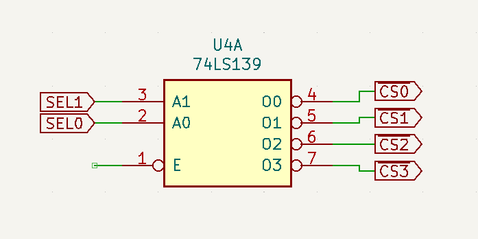
We will start by selecting 1 of 4 possible devices. We have already looked at using a 2-to-4 mux in our clock select circuit. This device takes 4 input lines and selects 1 of those lines as output via 2 select lines. Our device select logic, though, should actually be the opposite: we have a single "input" (we will discuss this later) that we want output on a single line out of a possible 4 lines. To accomplish this, we will use one half of a 74HC139 Dual 2-to-4 line decoder/demultiplexer (don't worry that the diagram states a 74LS139, it's being used here because it has the same footprint and function).
You may have noticed the deliberate usage of "assert" and "de-assert" when referring to turning on or off a device. This is because SPI is active-low to assert a device, not active-high. That means for our demux, our input would actually be a constant LOW signal and that LOW would flow out to the selected device. One nice feature of the '139 is that "input" is already assumed.
We also need a way of de-asserting all devices. In other words, we want all of the outputs to be HIGH. Another feature of the '139 is that it has an active-low ENABLE pin. When E is HIGH, all the outputs are HIGH. When E is LOW, the line selected via A0 and A1 is LOW.
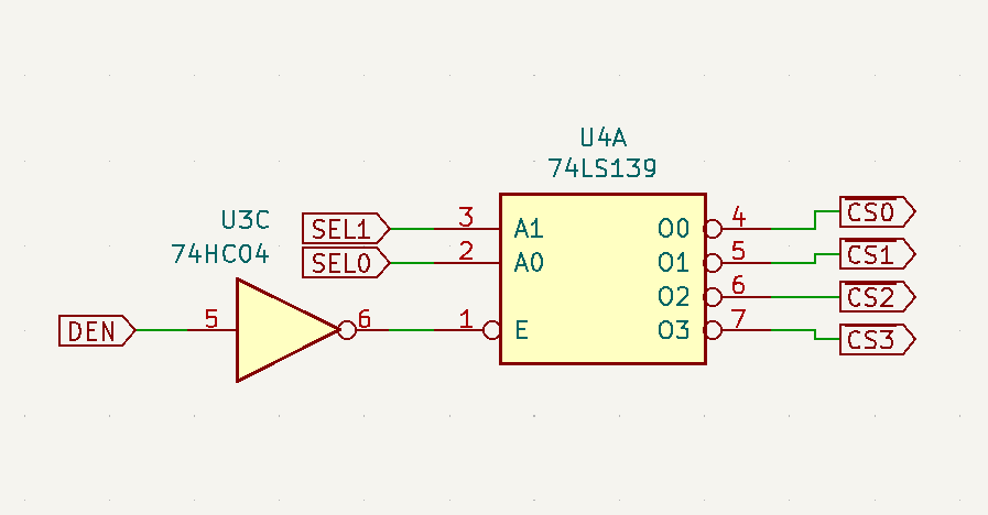
The intended method of controlling this is to use DEN. One consideration here is that on bootup, RES will go low and we want our control register to be reset. The 74HC273 we're using will zero the itself out, which means a LOW signal will be the default for DEN.
If we connect that line straight to E on our '139, it means a device (in this case Device 0 bc SEL0 and SEL1 will also be reset as LOW) will be asserted! This could be very bad as we don't know what will be on some of our other lines like CLK, MOSI or MOSI. So ideally, we want a LOW on DEN to mean de-asserted and a HIGH to mean asserted.
To do this, we will use one-sixth of a 74HC04 Hex-inverter. So our final design for the device selection logic is:
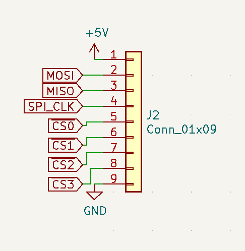
Lastly, we need a way to route our signals to actual devices. A simple and flexible way to do this is to provide a user port on the board. We haven't talked about some of the signals referenced in this circuit, but here is our port:
It provides 5V power and shared GND (only GND is truly necessary here. Devices can be self powered if they want to), MOSI, MISO, and SPI_CLK (these will be discussed when we talk about the data register) and our 4 device select lines.
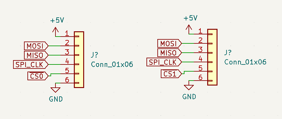
One interesting and perhaps nice change would be to provide 4 almost identical ports:
Here our shared lines are in identical spots across two ports but they each have a separate device select line routed. This would allow us to standardize connectors for our devices and provide power and ground to each device.
But for now, we will go with a single 1x9 port!
-
Part 2: Clock Select
07/01/2022 at 10:28 • 0 commentsOverview
The next subsystem we're going to examine is the clock select logic. SPI orchestrators and peripherals all share the same clock, generated by the orchestrator, to stay in-sync. Peripherals may only accept specific ranges of frequencies so the orchestrator needs the ability to generate a wide range of frequencies for better compatibility.
Remember that in our control register we dedicated 2 bits (so 4 possible values) to clock selection: DIV0 and DIV1 (Note: the target system for this device, the n8 Bit Special microcomputer, has a main clock of 3.6MHz):
DIV1...DIV0 Result Value @3.6Mhz 00 CLK / 2 1800 kHz 01 CLK / 4 900 kHz 10 CLK / 8 450 kHz 11 CLK / 16 225 kHz One side effect of this is that it is impossible to run the device at the full speed of the main clock.
Design Considerations
As previously stated, SPI peripherals may only accept specific ranges of clock frequencies and these limits are typically at higher clock speeds. SD cards, for example, can only be initialized in SPI mode under 400khz. Afterwards, they operate just fine in the Mhz range. With that in mind, this clock selector should be able to:
- operate under 400khz
- change clock speed via software
Design
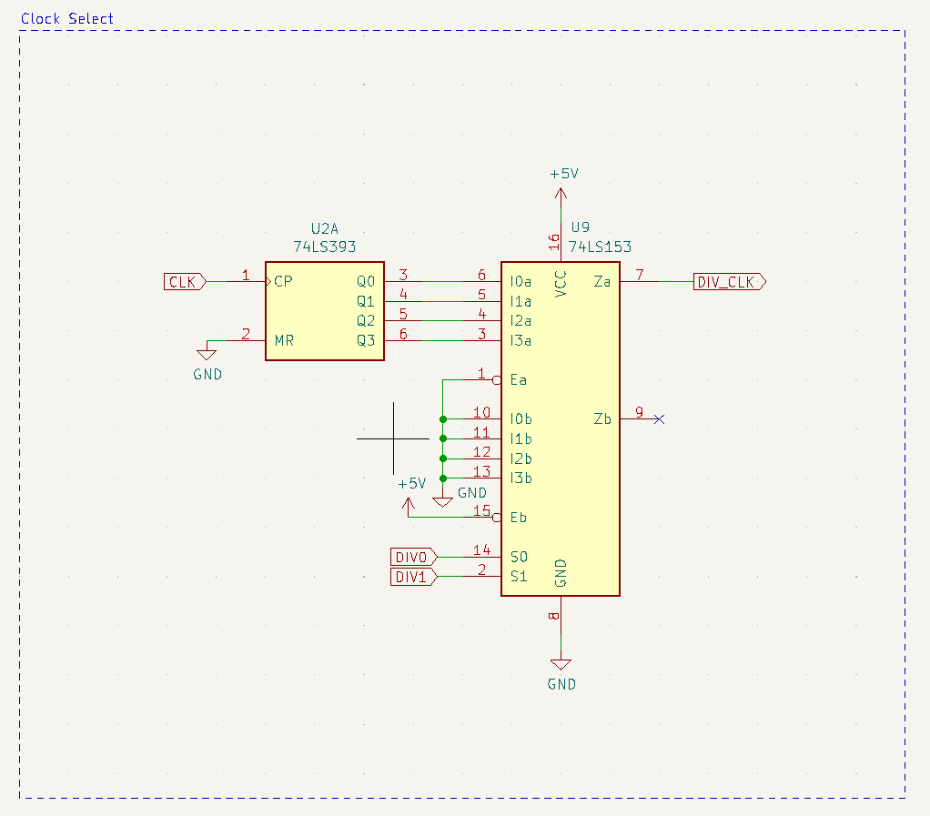
We will start with the circuit to generate our 4 possible clock values: the main clock divided by 2, 4, 8, and 16. You may see a very useful pattern emerge if you stare at those values long enough. Each value is half of the previous!
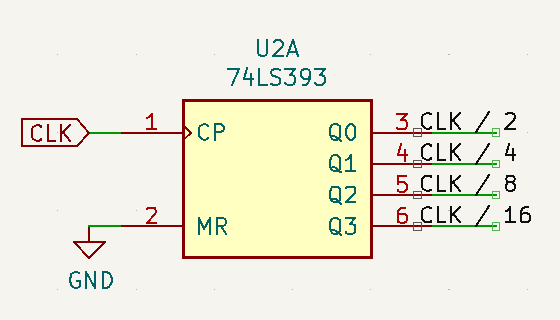
We will use this property to efficiently generate our divided clock signals using one half of a 74HC393 4-bit binary ripple counter. We will connect our main system clock to the clock input of the counter and each of the 4 outputs will be our 4 clock signals:
Note that we tied MR line to ground (this reset line is assert high!) so this counter will run continuously and cannot be reset. This has the potential side effect of the first pulse of the divided clock being too quick after changing the clock speed but this doesn't seem dangerous.
This device is also negative-edge triggered rather than positive-edge triggered like many of the other devices in this design. On integration, we will see if that is going to be a problem or if we will have to invert the incoming clock signal to better fit.
Now we need a way to programatically select which of these signals is our divided clock, using the 2 lowest bits in our control register. For this we will use one half of a 74HC153 4-input multiplexer. In essence, this allows 2-lines to select a single line from our 4 inputs, exactly what we need. The other half of the device is just completely disabled so there is no interference. So our final design is:
-
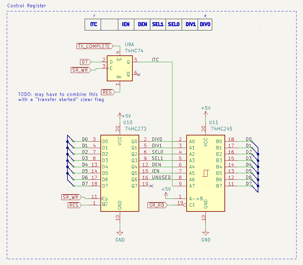
Part 1: Control Register
06/29/2022 at 15:48 • 0 commentsOverview
We will start our discussion of this design with the control register because virtually every other subsystem depends on it in some way. It is the primary interface for controlling the behavior of the device. To recap, the control register is an 8-bit read/write register and this is how its bits are laid out:
Bit 7 Bit 6 Bit 5 Bit 4 Bit 3 Bit 2 Bit 1 Bit 0 ITC x IEN DEN SEL1 SEL0 DIV1 DIV0 - DIV0 and DIV1 are a 2-bit clock divider select
- SEL0 and SEL1 are a 2-bit device select
- DEN is a device enable flag
- IEN is an interrupt enable flag
- Bit 6 is unused
- ITC is a transfer complete flag (it is also an interrupt acknowledge flag if IEN is enabled and a transfer has completed, thus triggering an interrupt)
Design Considerations
There are a few things to remember when designing this control register:
- it needs to fit in well in a 6502 memory-mapped environment
- it must be safe to read and write
- it must be resettable
- other subsystems are controlled via flag values so these have to be accessible to the rest of the design without driving the shared data bus
- on a completed transfer, the ITC flag (discussed in a future log entry) must be automatically set. This requirement causes much of the complexity of this design
Design
In discussing the design, we will add complexity layer-by-layer to address each of the design considerations.
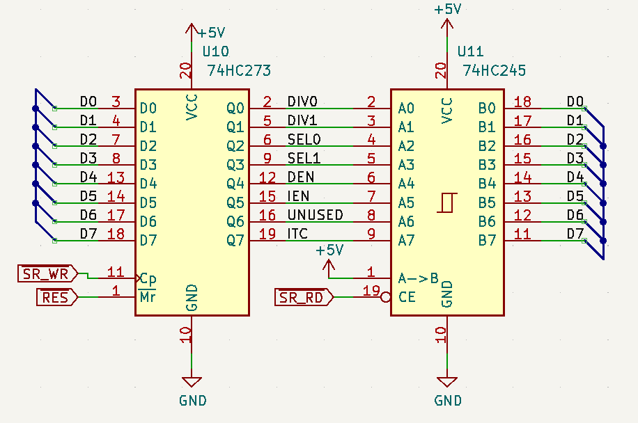
To start, we need a read/write register that fits well in a 6502 memory-mapped environment. For this basic task, I chose a 74HC273 Octal D-type positive-edge triggered flip-flop. This IC satisfies the first 2 considerations pretty well. It features:
- 8-bit input/output
- dedicated reset line
- data latch on a positive-edge trigger to its clock line
Unfortunately, this device by itself does not fit well in a 6502 memory-mapped environment. When SPI Master is not being addressed, it should be completely disconnected from the shared data bus. This particular chip doesn't have that capability.
One option is to use a 74HC373. This device has built-in tri-state buffers that can prevent the IC from driving the data bus, but this would break the requirement that other subsystems be able to read flag values when the device isn't asserted.
The solution I've chosen is to use a 74HC245 Octal bus transciever. The '245 is configured to permanently flow in one direction, A -> B, where A are inputs and B are outputs. Next, the '273 outputs are connected to the '245 inputs, and the '273 outputs are connected to the shared data bus.
Other devices can connect to the lines between the two ICs, thus satisfying that design requirement.
Only one requirement remains, which is the ability to set/reset the ITC bit independently. This requirement is the most complex because in many cases, to the system, it should just look like a regular 8-bit register. You write values to it, you can read that value back. But in certain scenarios, when a transfer is complete (and potentially when a transfer is started), the ITC bit should be set (or cleared, respectively) by the device itself.
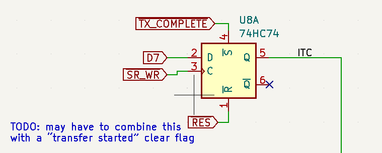
To satisfy this design requirement, I've chosen to break the top bit out into its own device, one half of a 74HC74 Dual D-type positive-edge triggered flip-flop. This flip-flop has separate set and reset lines and is triggered at the same time (when their clocks are connected to the same signal) as the '273.
On startup, the RESET line is driven low and the value is 0. When a transfer is complete, TX_COMPLETE is driven low and the value is set to 1. Otherwise, the user can write a value to it on D7 as part of a memory write or can read the value on D7 as part of a memory read.
This could bring a potential failure point (or quirk at least) because you can write a 1 to this bit and tell the device "transfer is complete". This would kick off an interrupt if enabled, etc. One solution to this is to disconnect D7 from the input side, but you would need a way to acknowledge an interrupt and clear ITC from the programmer's perspective. The venerable 6551 ACIA does this by clearing the interrupt flag when the data register is read. That is something to explore, but for now, the programmer can clear ITC (and thus acknowledge the interrupt was handled) by writing a 0 to this bit in the control register.
Putting it all together, this is the "final" design for the control register.
Q7 from the '273 is disconnected from the '245 and instead Q from the '74 is connected. We will address the 2nd half of the '74 and how the various signals referenced (SR_WR, SR_RD, TX_COMPLETE) are generated in later posts.
SPI Gate
An SPI interface for 6502 microcomputers using discrete logic gates