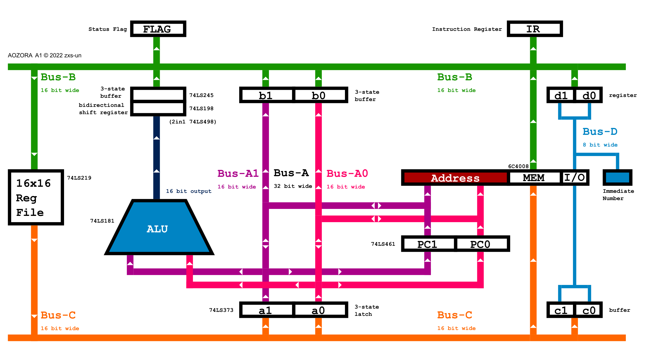
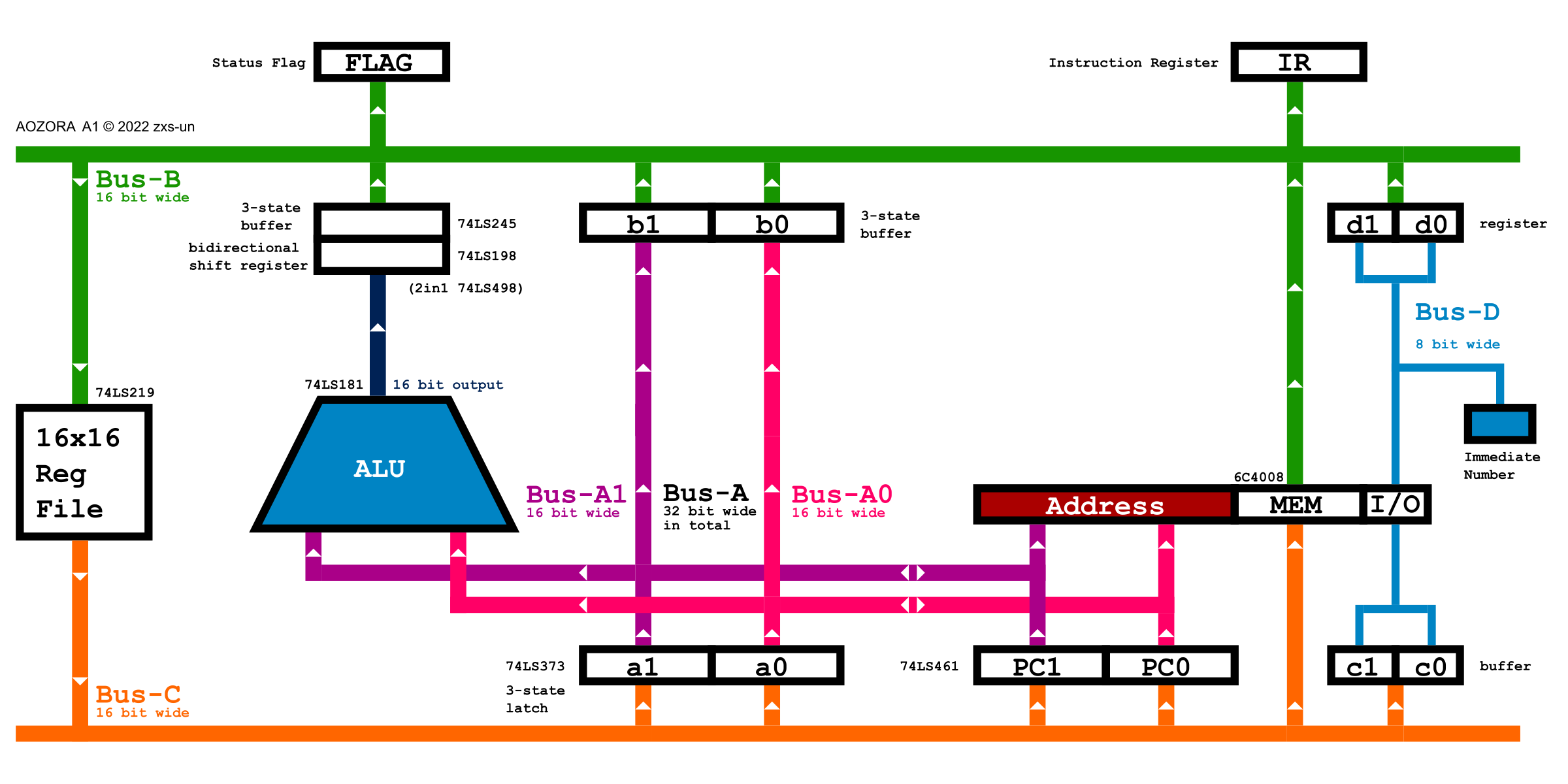
With just a flash in mind, being not a professional and starting from zero, after 3 weeks of search and learn, the bus architecture design for A1 finally came out.
At the very first beginning, project AOZORA was targeted to implement the Ibex RISC-V RV32EC core with mainly 74-series TTL ICs on solderless breadboards.
After reading project Pineapple ONE, support for RV32EC was abandoned, since a 32-bit computer requires a lot more ICs than a 16-bit or 8bit computer, as well as the 32-bit bus might be too wide to implement on breadboards.
Data bus width was finally decided to be 16-bit, and address bus to be 32-bit.
First version of the bus architecture design for A1 is mainly inspired by the famous 6502, and was hugely influenced by load-store architecture commonly seen in RISC architectures.

Just one day after the bus architecture idea on paper has been redrawn with software, when reading amazing home-brew computer projects on Hackaday, 2-Zons' project 8 Bit Breadboard CPU showed at SIMILAR PROJECTS.
After looking into the block diagram of that project, it is clear that A1 shares a very similar bus architecture with that project.
So the bus architecture for A1 got some refinement inspired by that project and thus comes the second version.

Bus architecture design is now almost complete, though a comparator might be needed alongside the ALU and the address decoder might also need design in detail. Focus will be put on designing controller unit and instruction set then.
 zxs-un
Discussions
Become a Hackaday.io Member
Create an account to leave a comment. Already have an account? Log In.