 jaromir.sukuba
If had more time for PCB production, I'd send it to itead or oshpark, but unfortunately this wasn't the case. On the other hand, friend of mine has CNC milling machine, which can be used to mill out the PCBs. This process isn't that fine as th usual 0,15/0,15mm rules, so I had to rework my PCBs to fit his requirements. What more, single-sided PCBs are somehow better for CNC manufacturing than double-sided, so I had to take this aspect into account and design single sided PCBs. After a good hour of optimizing things, I got this
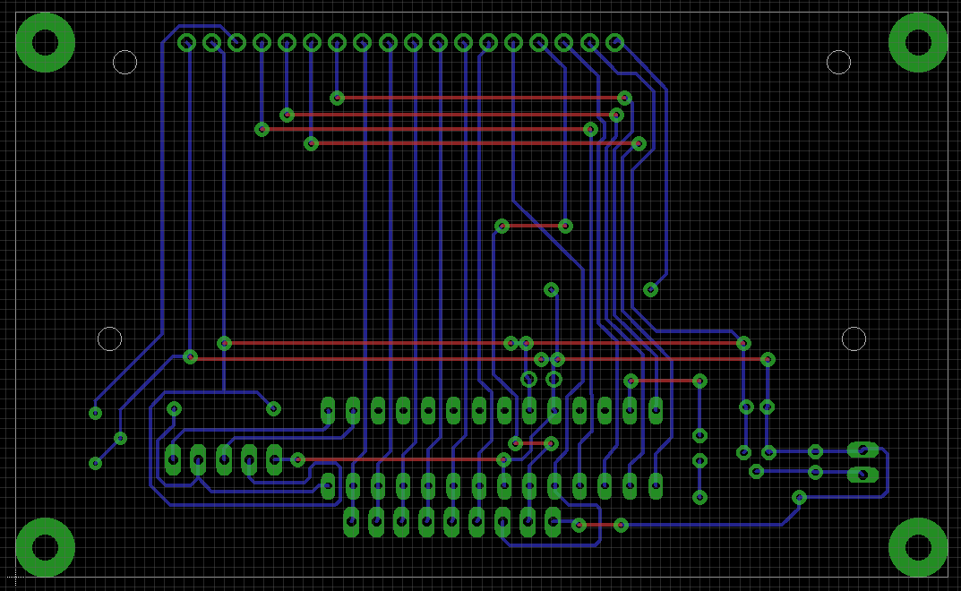
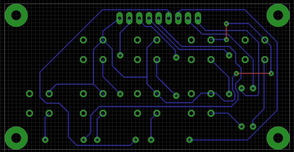
Blue lines are copper traces on bottom side, red ones are projected to be wire links on top side. Keyboard PCB was un-double-sided too
And I also designed FR4 enclosure for the thing
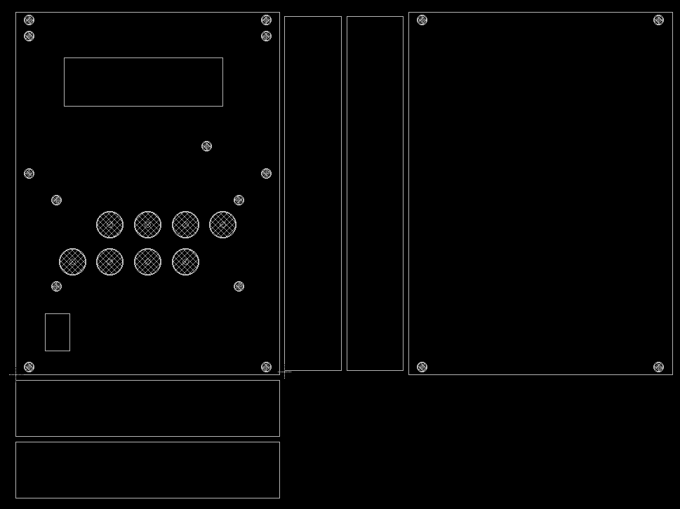
Great thing about home-made PCBs is the development cycle speed. Next day I had my PCBs prepared - the enclosure
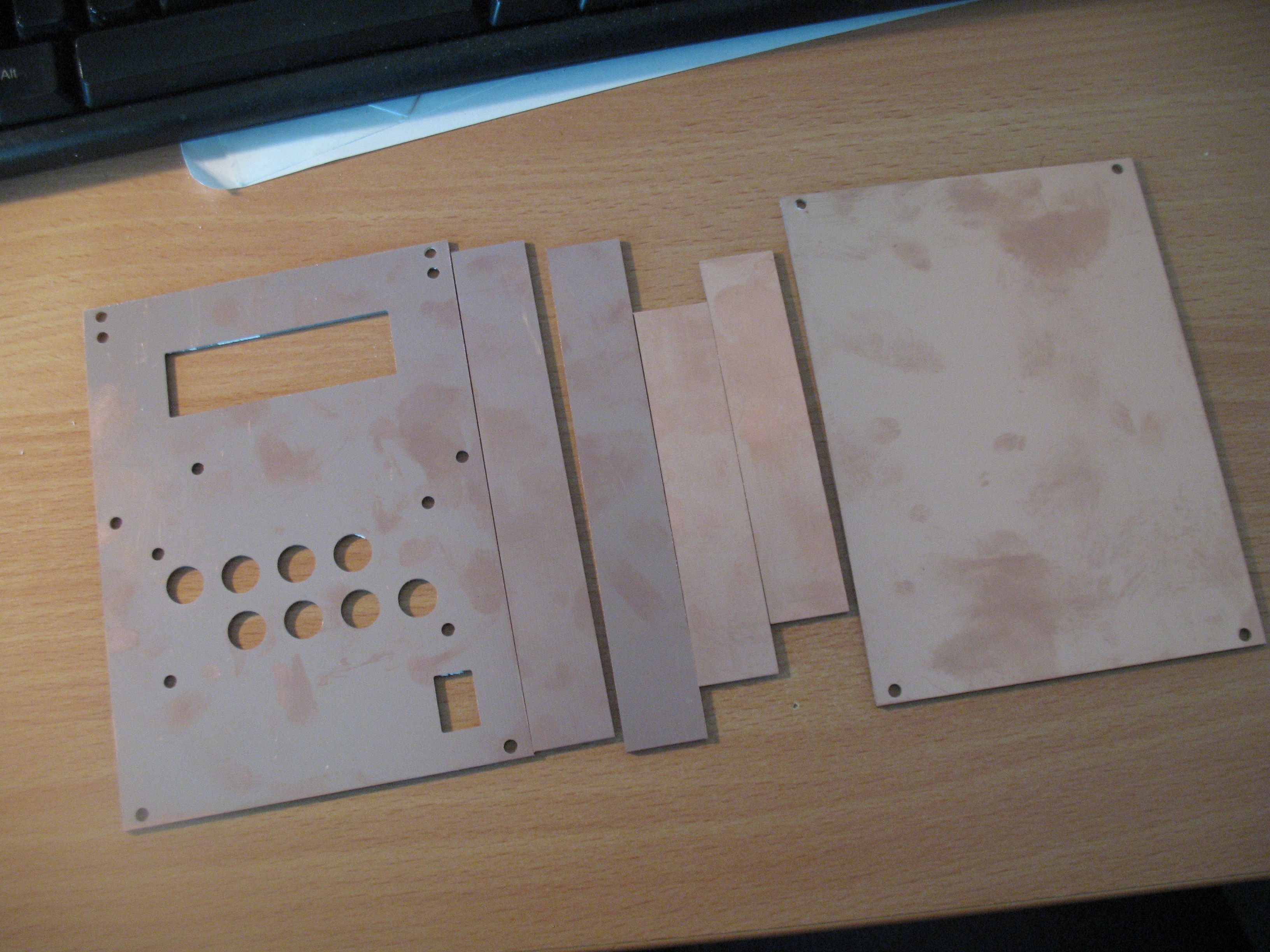
as well as the "functional" PCBs
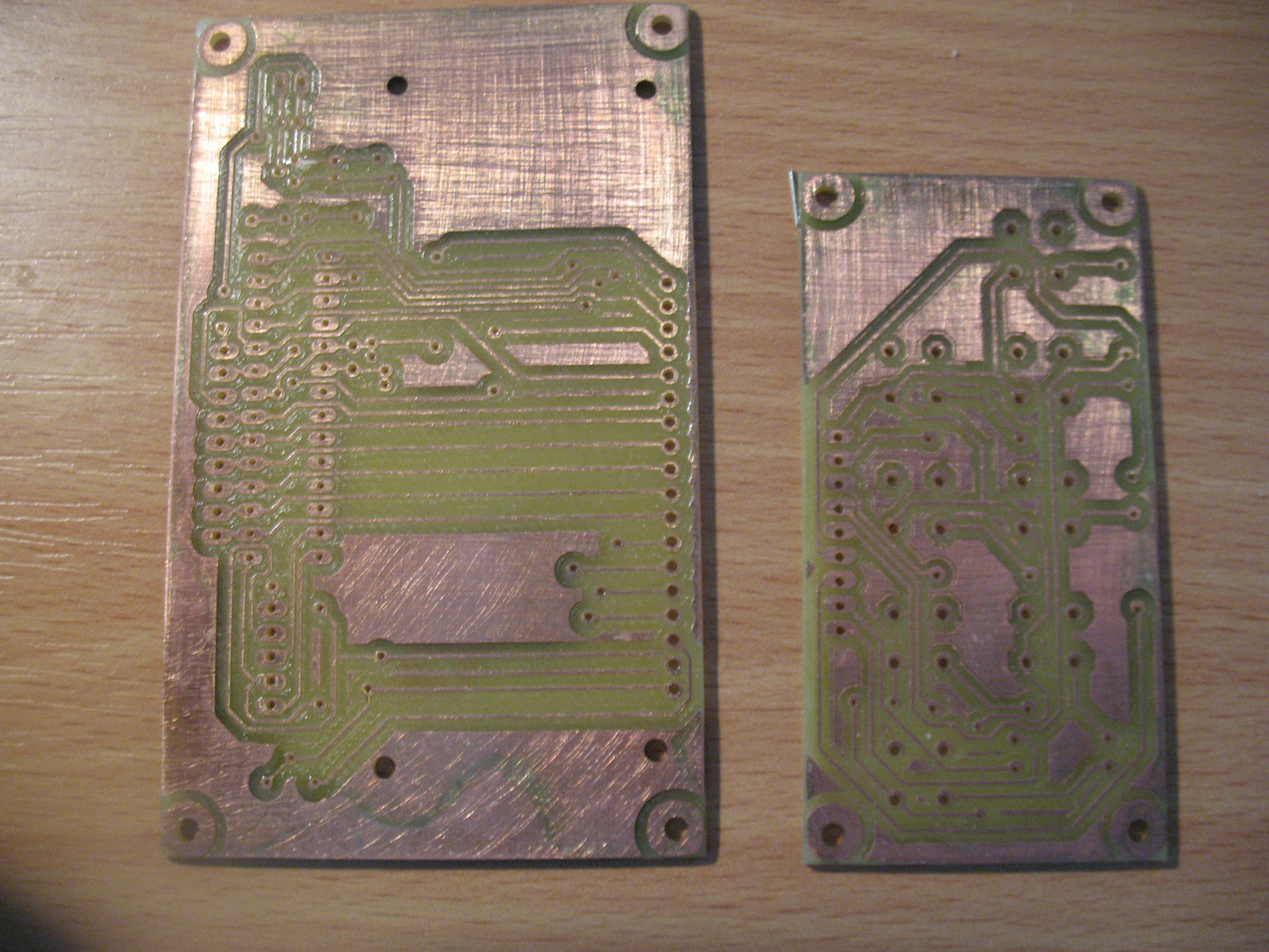
The PCBs look a bit dull on the photo, as I brushed it and covered with solution of colophony with acetone, to stop it from oxidizing and help with soldering. In reality it looks better.
Discussions
Become a Hackaday.io Member
Create an account to leave a comment. Already have an account? Log In.
Wow, those traces look really thin to be milled. Maybe I just didn't realize how good PCB milling is these days, but I somehow thought the traces needed to be really fat and widely spaced. What design rules are you able to use?
Maybe there's a PCB mill in my future...
Are you sure? yes | no
The design rules we agreed on and I entered into DRC were 0,3mm track width, 0,4mm isolation, 0,3mm drill size.
The accuracy of modern - yet still cheap - CNC mills is surprising. While it could be even better, aforementioned specs are easy to achieve with no special precautions and minimal setup.
Are you sure? yes | no