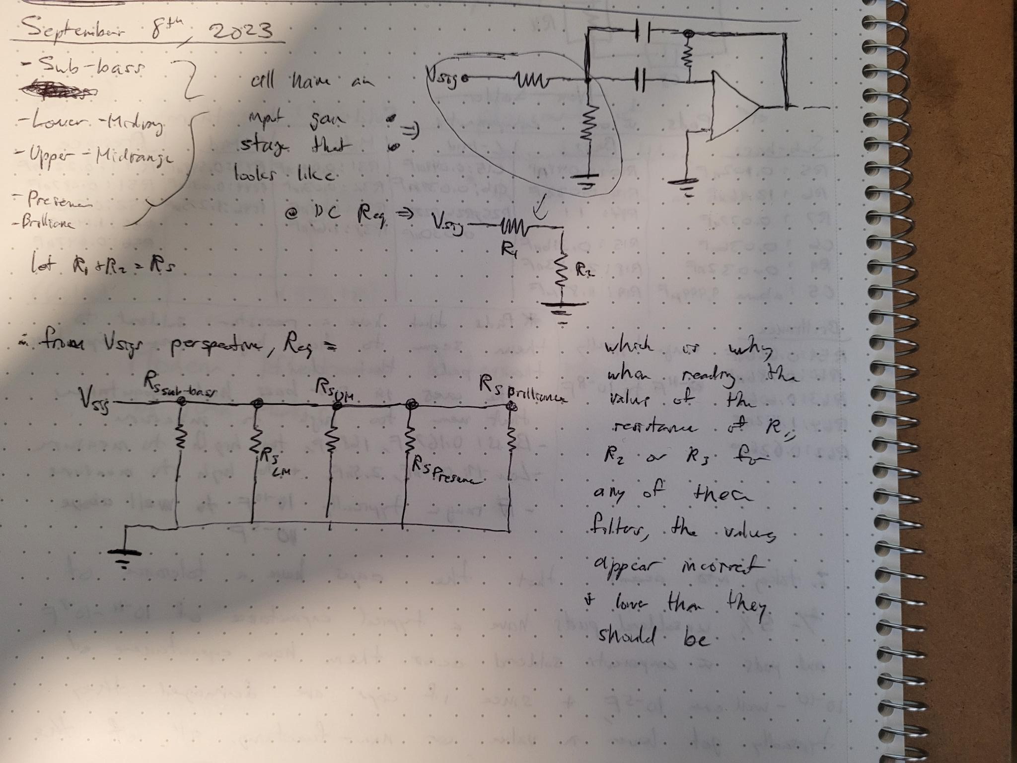
Design flaw, the first stage resistors connected to Vsig of the Sub-Bass, L-Mid, U-Mid, Presence and Brilliance filter have a topology that make that appear in parallel with each other when the resistance is measured between Vsig and ground. As a result this significantly lowers the resistance measured by those resistors as shown in the following diagram.
This means that the spectrum filters are not isolated from each other and will affect each other's signal responses
****************To prevent this problem, I am going to use the fourth op-amp in each IC package as a buffer amplifier for each spectrum filter
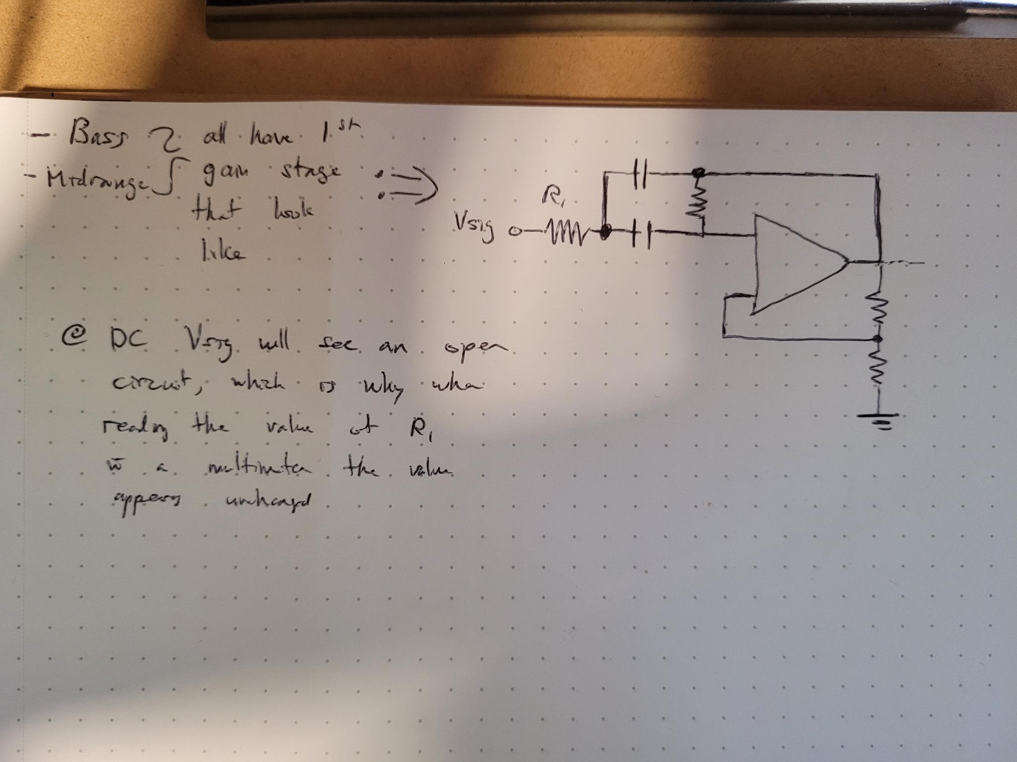
The first stage resistors of the Bass and midrange filter connect to Vsig and a capacitor as shown in the following diagram. Therefore the measured resistance was unaffected as shown in the following image
Interesting, the resistors
that appear to be defective are at the first stage of their respective
spectrum filters and connect either directly to Vsig or via one resistor
***Figured out the issue,
this resisters are not defective, this is a design mistake, need input
buffers will go into more detail tomorrow
Analyzed measured capacitor
values, will go into more detail tomorrow
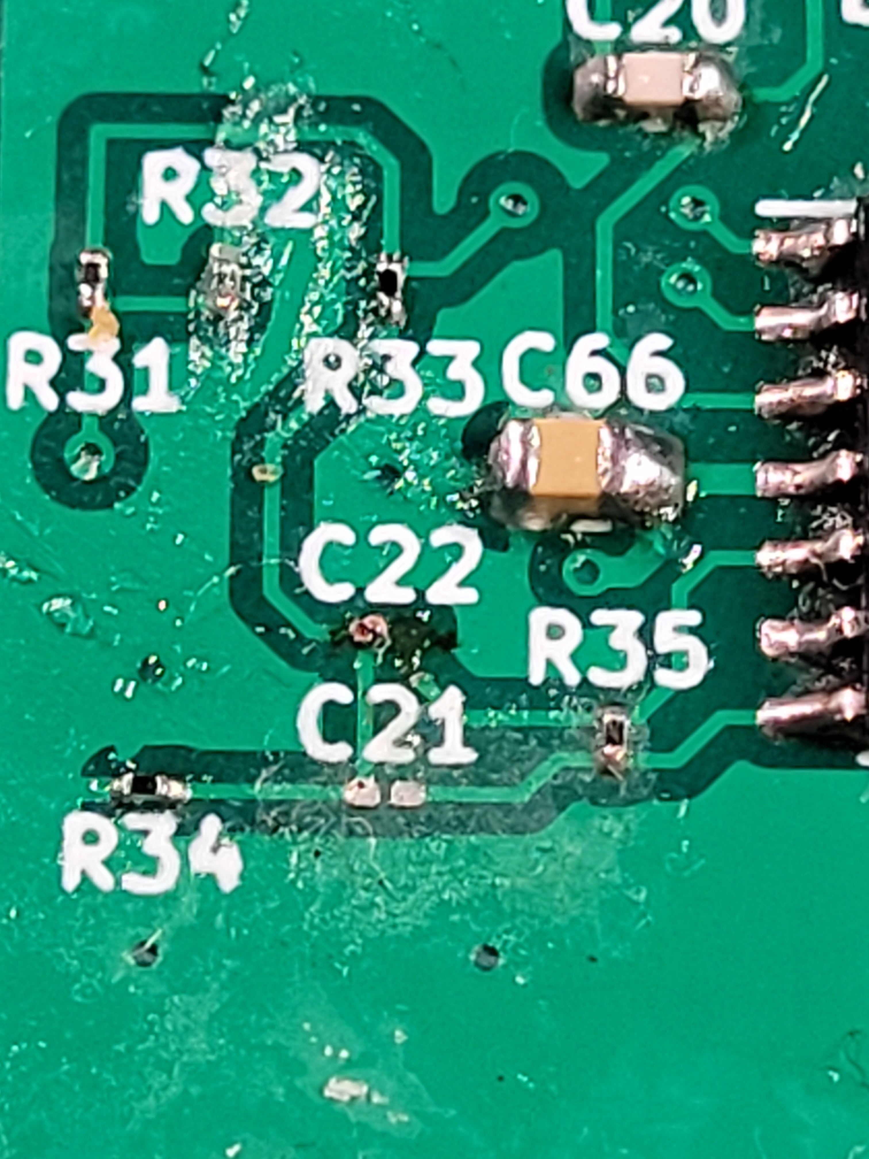
Attempted to solder capacitor
onto area with broken pad by soldering to the trace after scrapping the
protection off
Was able to scrape
protection off, but was not able to get solder to stick to the exposed
copper
Ended up making the
situation worse
The whole point of soldering
myself was to:
Save money
To be accurately claim that
I can solder surface mount devices
The above two are no longer
issues
**SOLUTION: Redesign the board
Don't use components smaller
than 0402, use 0603 if space permits
Fix negative voltage
regulator output and feedback mistake (would have to cut 2 traces and
connect 2 traces...)
Re-check every other circuit
for mistakes
This works out as I can
easily solder 0402 sized devices now, a lot of my 0201 components got
damaged and have values that deviate greatly from the ideal value, so the
filters were not gonna work properly anyway
I have all of the tools I
need this time, should be able to finish soldering aspect within a week
I will spend the rest of this
week and the weekend redesigning and working on the BOM, aim to order new
board by Sunday or Monday
***Incorporate component
availability into design - check if JLCPCB has component before selection,
will use soldering
Will buy new IC's as well,
large chance of damaging components with hot air rework station, do not
wanna take the time and risk with a board with this many components
 Ghani Lawal