PDP-11/70 replica
Recreating boards for those old computers, and improve on them
Recreating boards for those old computers, and improve on them
To make the experience fit your profile, pick a username and tell us what interests you.
We found and based on your interests.
It's been a while, lots have been happening at $dayjob, and time has been an issue lately (that, and funds for components)
I had ordered boards from PCBWay back in february, received them some time later, then time-crunch hit, and I had no time whatsoever to do anything on the project.
those boards are beautiful, look at them !
and here is the stencil...
Again, thank you very much to PCBWay for sponsoring this project with their PCBs
Now, I need to scrounge some money to give to DigiKey 🤣
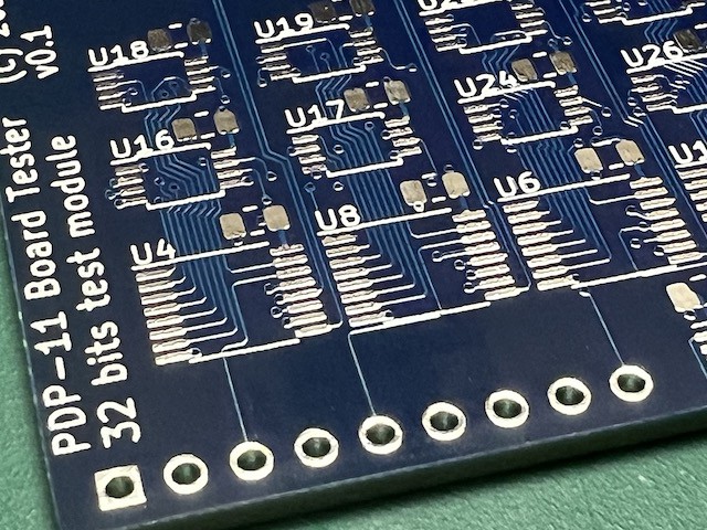
Started designing an automated board tester.
I don't know what computer I should use, a Raspi Pico should be sufficient, but a full raspi could be better, dunno.
the video is here
There, I started to populate the DAP board, unfortunately, I am missing the 50-ish 16 legged sockets, so those will have to wait.
see the video here
Finally found some time (and money) to order the DAP boards from JLCPCB.
here they are in their purple glory (each part of the CPU will have a different color)
I started to assemble them but I messed up the reference of 2 resistor values in my digikey order, so I'll have to do another order for those...
Took some time today to install all the small components -- Resistors and Diodes -- on the chip tester pcb
will do the rest another day, i't getting too hot , have to turn off the light and soldering iron
In order to make sure everything works, I have ordered a Retro Chip Tester Pro from Stephan
https://8bit-museum.de/sonstiges/hardware-projekte/hardware-projekte-chip-tester-english/
which I just received.
Time to order the components to fill this very nice set of boards !
I made a new component for the board and gold fingers, and modified the first board to use it.
Also, I dumped it all into a new gitlab project.
enjoy !
I'll be ordering boards when some money shows up. will have more pictures then
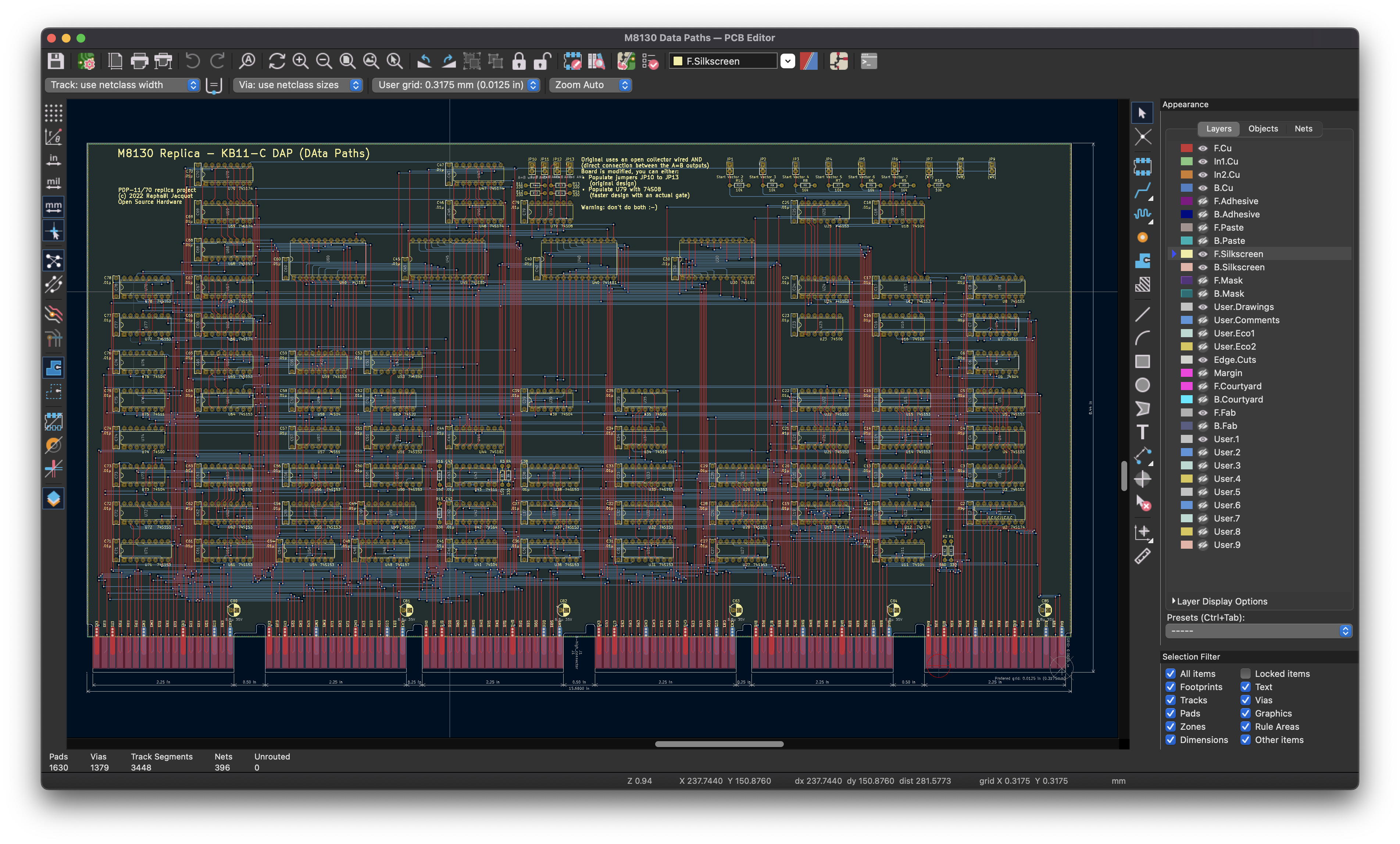
There, took some time, but the first board (the DAP, DAta Paths) is fully routed
Turns out I was mistaken with the A=B situation.
The pins on the ALU are open collector, this does a wired AND, which is incredibly slow (as suspected).
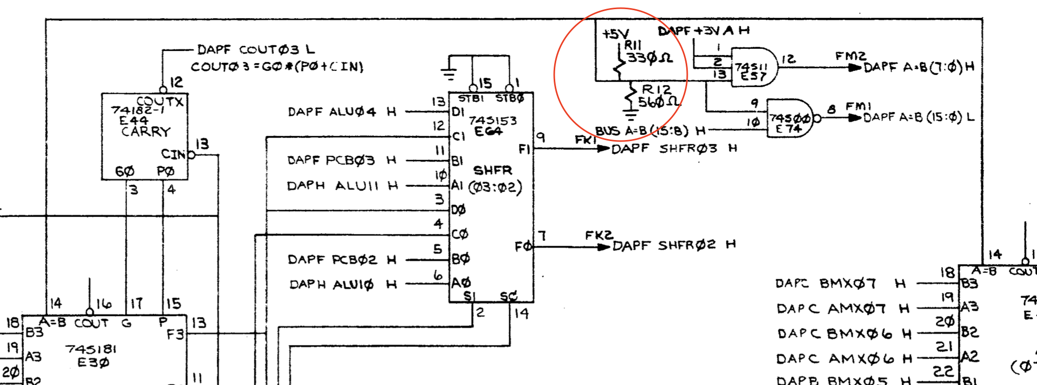
So, what I had needs modified, and this appears to be more appropriate. The R11 / R12 value is debatable though, maybe the classic 1k value would be good enough ?
So, how do we go on doing this ?
Well, download the document here for the KB11-C processor boardand start page 1 😎
First board is the M8130 DAP (Data Paths) which contains the 16 bit integer ALU and related multiplexers.
Schematic capture is done.
There is one thing that looks wierd to me in the original schematic, namely, the ALU chips (74S181) A=B ouputs are tied together with a pair of resistors to pull the line up/down, sure looks like a wired or hack...
So I decided to add the possibility to replace this with proper or gates (a 74S02 would add 5.5ns, which I don't think is so much delay that it'd break things)
Same thing happens in the generation of "BUS A=B (15:08) H"
Of course, the board could be populated with more recent parts such as ACT for all functions that currently exist in this family.
I have now started routing the board. about 50% done right now.
Create an account to leave a comment. Already have an account? Log In.
4 layer is a must with fast ttl. Don't even think 2 layers. You need good ground and power planes.
Can supply me any schematics of other boards?
@raps500 for the connectors, there are 3 options:
* edac
* sullins
have both something suitable
there's also https://ecsconn.com/ProductDetails/2400-Series-Card-Edge-Connectors-125-125-Contact-Spacing-Dec-Style-Press-Fit.html however it looks like they are rather expensive.
Very nice boards, where the originals 4 layers ? with so much empty space I'd probably go for 2 layers, at least for experimenting. Are you planning on using shottky parts ? The 11/70 is quite large, I wonder if something like the 11/05, which should be 2 boards, couldn't be a more startup approach (thinking aloud). I assume you have access to a 11/70...
I don't know if the originals were 4 layers.
I'm planning on using 74F parts, they are somewhat still available, just about as fast and consume much less than the original 74S
I have no 11/70 available to me, i'm just going by the original schematics (customer print)
how about the edge connectors ? DEC used some with staggered pins, are they still available ? which one are you planning for the backplane ?
That is a pretty generous sponsorship! those Unibus boards were close to the size of a lunch tray.
Open collector zero after the result was incredibly slow. 74181's A=B when all inverse F's are high on any zero result, not strictly equality. This pin's function was poorly named. You need external AND to merge internal ANDs, rather than NOR as you have drawn. This old ALU could work at least 40% faster by not waiting on those terrible open collectors. Roll your own zero from F pins instead.
oh, that's right those pins are labelled open collector on the datasheet...
so, what I really need is pull each of the a=b outputs, and an and gate...
should the pull-up/pull down they use be replicated, or just a pull up to VCC ?
Forget those slow A=B gates exist and use something better.
Your choice to AND then AND again, or NAND then NOR.
74AS series might be a good choice, still made today.
Unused 74181 open collectors need no pull-up.
Become a member to follow this project and never miss any updates
All my testers need loads of memory for all the scripts for user interface. Speed was not a problem. The part under test always needed time to settle. I use a Tek 132 channel logic analyzer for fast measurements. You could programme one up to monitor inputs. Just a thought.