-
Ø0 FTW!
05/11/2022 at 16:03 • 0 commentsI can happily confirm that even on the NMOS 6502 Ø2B can be replaced with Ø0 if Ø1B is replaced with ~Ø0.
This improves margins a bit and solves an issue on the NMOS 6502 that caused a few spurious writes - I guess my NMOS Ø2-pullup was not quite enough under all conditions.
Either way - this is why R1 has three of the jumper positions next to the barrel plug.
For the next revision this means I will probably throw away the buffering and just use Ø0 and it's inverted companion. I still need the 74'14 for the reset circuit - but having four left over inverters is great!
-
The mental perils of pin sharing
05/05/2022 at 20:13 • 1 commentThis one might get... technical. I will probably share the light version in a future video. TL;DR - I made a better PS/2 interface but got greedy while optimizing.
Let's start off with a success.. I did it! I actually did it! I got rid of all three components for interfacing the PS/2 keyboard, I got back all of the 6522's port A, including CA1 and CA2, and all it took in return was one half of a 74hc74, some time on the 6522 VIA shift register... and PB6.
This magical pin can count negative pulses and only interrupt the CPU after x pulses have passed. Since the shift register on the 6522 insists that 8 and only 8 shifts is the correct number of shifts for an IRQ, PB6 can take over this job of counting the shift register clocks(together with CB1 - not replacing it) and suddenly the shift register can be used to filter out the correct 8 bits of an arbitrary number of bits. For PS/2 - this number is 11.
You might say I'm throwing away the parity, start and stop bits for no reason, and sure - that can probably be avoided with this trick as well - but I chose the extra complexity and IRQ's aren't worth it for now. And luckily it's only a software change if I decide I need the error checking bits later - I can use the SR IRQ for the first eight bits and grab the remaining three with the PB6 IRQ, or even alternate the number of PB6 bits.
The reason I need the 74hc74 between the PS/2 clock line and CB1 shift register clock is two-fold. First, all 6522's have a bug where external shift register clocks are ignored if they coincide with the falling edge of PHI2, hence the 74hc74 can save the day by only changing the PS/2 clock line on the rising edge of PHI2. Crisis avoided. Second, the inverted output of the '74 is better suited as the clocking edge for PS/2 data since it should be sampled on the rising edge instead of the falling edge. Yay for free inverters!
And best of all - since PB6 is on the keyboard side of the '74, it can be used to hold down the PS/2 clock line and initiate computer -> keyboard data transfer, with a simple mode change of the shift register! Yay for blinky lights on keyboards!
You might have caught on as to what perils the title of this post refers to by now... PB6 is already in use on the board. Not only is it in use, it's also an output, instead of an input.
So far I've been using it as the MISO pin for SPI and that's worked out fantastically since it's pretty fast to sample pin 6 with the BIT instruction - so SPI might be slow, but not really that slow considering it's supposed to be a "late 1970's computer".
I couldn't let it go though. I tumbled down the rabbit hole as I tried to multiplex the poor PB6.
In theory very simple - just leave the pin as an input for the PS/2 clock while not using SPI and then toggle it to an output when it's time to use SPI, right?
Turns out it's not that simple to juggle code, when you not only have to toggle the data direction register but also have to make sure the shift register isn't clocking while using SPI, and you also have to make sure T2 isn't counting down from PB6 edges, and you also have to make sure the right interrupts are disabled... And then do it all over again to enable the disabled things after every SPI byte..
After the success of saving IC's and ports that was previously tied up for PS/2 I couldn't just let it go though, and I was thirsty for more. .. I didn't want to take up another PIN! ... so I started juggling, I started debouncing my polling of the nRF24l01 circuit, I started littering the ROM code with resets of the T2 counter, I left in extra SEI's and CLI's, I was seeing my screen fill up with misaligned characters, the keyboard not working, then working, frantically enabling debug output to the screen... And getting no help.
And here I am. It's over. I will cut the traces to MOSI and MISO tomorrow. MOSI is going to PB7 where it will later share it's time with output to the tape interface. MISO is quietly moving over to the unused PB5 I have no idea what I was saving for. Yay for jumpers!
And the code I have so desperately tried to fix and save? A BIT and a BPL, has turned into an LDA, an AND and a BEQ for a total of two 2 MHz cycles extra.
Let this be a reminder: Don't spend hours trying to save one microsecond. You might be able to save the microsecond - you will never get the hours back. -
Why the external keyboard interface?
04/14/2022 at 19:25 • 0 commentsWhen designing a SBC you always have to balance features vs board space vs price.
When I realized I had to make a choice between putting in the time and finding a new solution to a problem many smart people have already worked hard at or throwing what I knew worked on the board I chose option number three: Make it an add-on - for now.
![]()
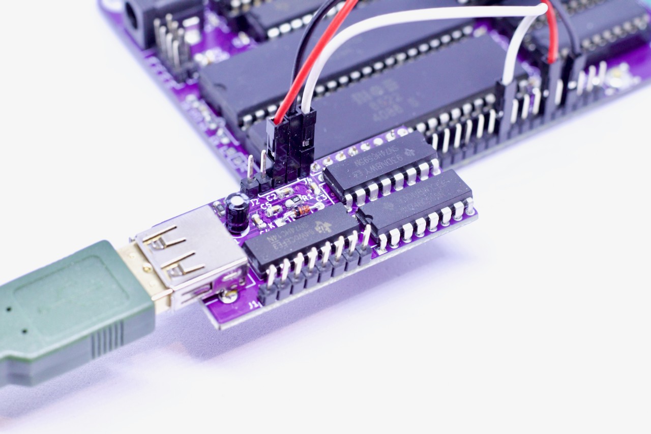
It's a slight redesign of Dieter Müllers PS/2 interface (warning: Files require OOOLD version of Eagle) which I heavily suspect is what Ben Eater based his version on.
I don't know if Dieter tried to obfuscate his design on purpose, but he certainly used a lot of gates for seemingly no other reason than buffering. Like Ben I also used two '595's but got the 74HC14 gates down to two instead of three - so if I ever need four Schmitt-Trigger inverters they're in a handy place.
It plugs right into PORTA and just needs the signal to CA1 wired over, along with 5V and GND.
But.. Even if it just uses two inverter gates and two shift registers it just seems wrong to throw hardware at a software problem in this case (even though I'm usually not opposed to that).
It really should be possible to, at the very least, do the shift registers in software if not with the 6522 shift register. Since the 6522 can count pulses on PB6 and generate IRQ's it should be possible to use that to overcome the limitations of the 6522 shift register.
Either way - the PS/2-interface is external for now because I know it can be done better, or at least cheaper. And just maybe without taking up more board space.
-
The story of the NMOS PHI2 pullup
04/13/2022 at 16:58 • 0 commentsThe cute little jumper wire in the photo below has a 1200 Ohm resistor on one end and pulls phi2 high.
You see, when I was testing R1 with different 6502's most of them suddenly worked horribly, RAM got corrupted, screen was displaying garbage, and most of the time it would just crash. When I put my scope on PHI2 the news was not good. Instead of showing a nice 2 MHz square wave, what I got was basically a shark fin pattern. A slow rise, up to about 4.7 Volts and then a reasonably fast drop.
When I asked on the 6502.org forum, the guesses ranged from "it's normal" to "you might have a defective internal pullup" - of course with a detour to "something is loading it"-town.
![]()
It turns out three out of the four 6502's I tested were NMOS and the one that worked was a CMOS variant. Since they were all sanded and relabeled(I wish they would stop that stupid practice! Especially for chips where a particular model may have sentimental value) I had no way of knowing.
Somewhere along the way I managed to get my glue timing skewed just enough that it would only work on a CMOS 65c02 with nice sharp edges for phi2 - and adding the extra 25ns from the slow rise, even though I ran it through a schmitt trigger inverter, completely broke the RAM write timing.
The solution here turned out to be adding a little bit of help to the internal phi2 pullup resistors with an external pullup. Anything over 1k2 Ohms didn't make much of a difference, so that's what I chose, since we want as little current flowing as possible when phi2 is low.
It still doesn't give me the nice sharp phi2 of the CMOS variant, but it certainly saves enough precious nanoseconds that the whole board - which is supposed to be NMOS compatible - works with both types.
For a later revision this will certainly get it's own pad so you don't have to jumper a resistor, but better yet would be to fix the issue of phi0 vs phi2 timing.
For now - this pretty little thing is required for correct NMOS operation.
-
R1 reset and clock considerations
04/13/2022 at 13:16 • 0 commentsThis is another one of those things where I knew better, but still decided to leave it out of r0.
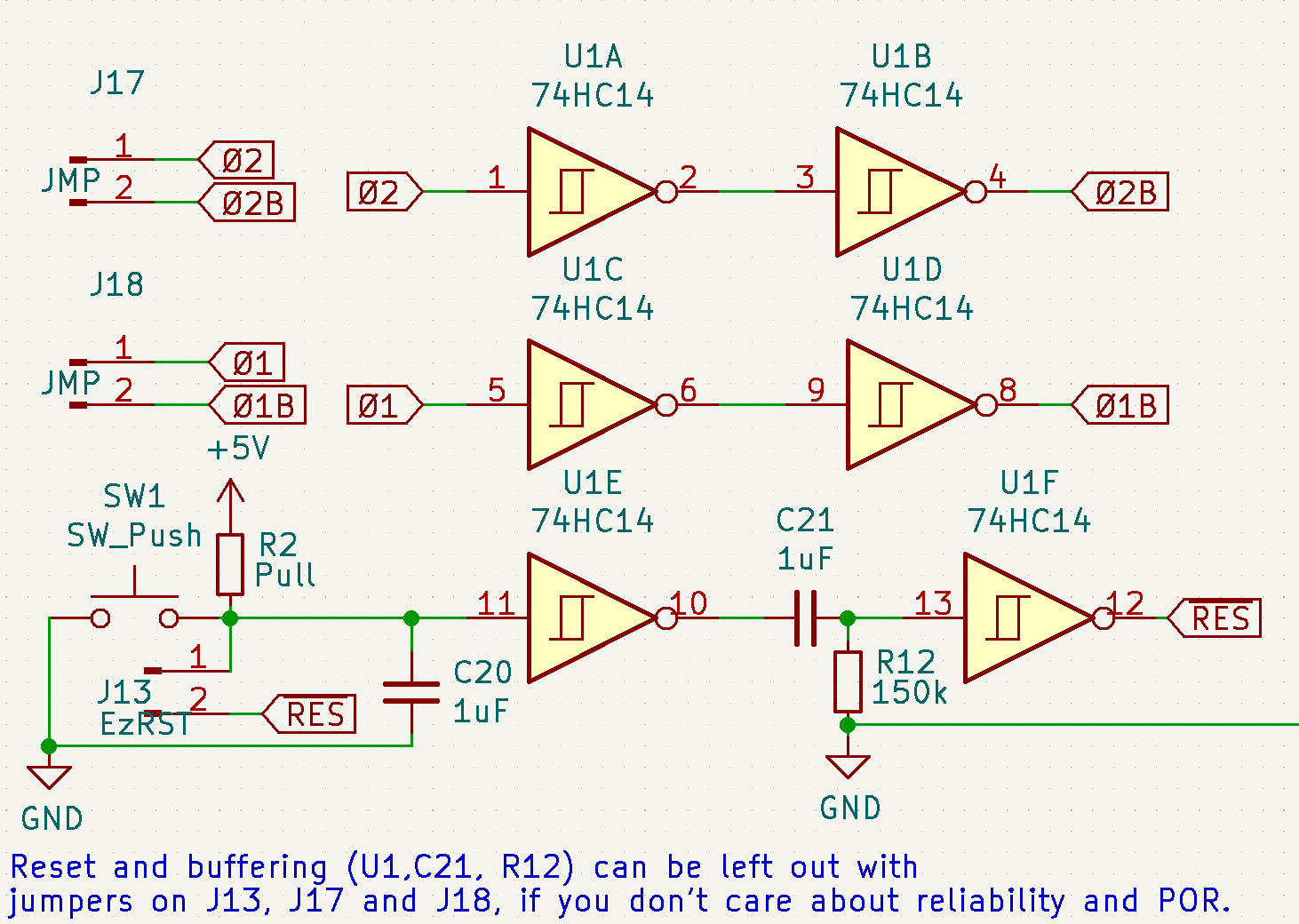
Thankfully I came to my senses and went for it: A semi-proper reset circuit. I had a close look at Garth Wilson's reset recommendations but decided against going all in with 555 timer monostables or DS1813's(wow those are expensive for what they do!)
Instead I went with Garth Wilson's design for NMOS 6502's but removed a pair of resistors and a diode to simplify things. As far as I can see the 1uF cap. and the first stage Schmitt-Trigger inverter is plenty of debouncing and a diode on the second inverter input seems superfluous as the input itself should already have protection diodes as part of the ESD protection.
![]()
With regards to the clock buffering, I simply double invert phi2 and phi1. This is to prevent loading of the clock outputs of the 6502...
... but actually it's not even recommended to use the two clock outputs for anything at all. However since I had a lot more luck using them for my video bus sharing, than using just the 2Mhz input signal a.k.a. phi0, along with the inverted version, I decided to leave the circuit this way until that issue is resolved.
When testing R1 I was very happy I did it this way, since it lets you test new clocks without cutting traces and soldering jumper wires. By simply leaving out U1 and placing a jumper on the reset line J13(which falls back to a slightly debounced reset signal) it's easy to feed the two clock lines with a different signal - for instance phi0 + phi0 inverted.
As a side note I think the reason it doesn't work to just use phi0 and ~phi0 is two fold:
1) Phi2 is about 30-50ns delayed compared to phi0, but the 6502 operates(including data and address line timing) according to phi2. When using the data bus 100% of the time this is a problem when it's driven up to 50ns out of phase on one side.
2) Phi1 & phi2 are not 50% duty cycle - the high time of both are a little bit shorter than the low time, which decreases the issue of bus contention.
Worst case this means I have to make a phi0 derivative that's synced with phi2 and also has a shorter high than low time. For now this seems like too much work to fix a hypothetical issue, but I'm happy it's possible to test without hacking off pieces of the PCB.
That's about why I added this little part - and if you're short one 74HC14, you can still use the computer without it by adding the three jumpers. -
So what else is new?
04/08/2022 at 14:16 • 0 comments...continued.
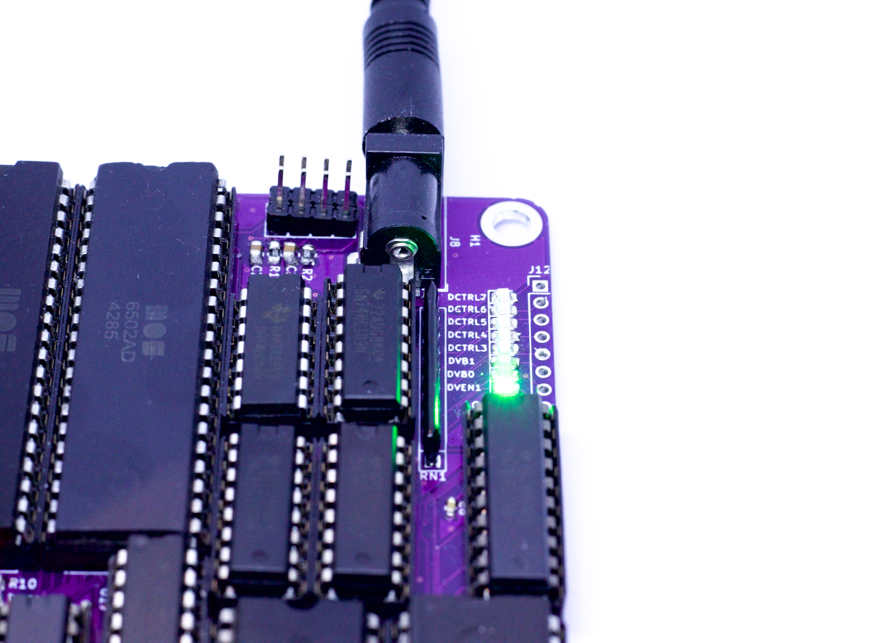
In r0, the 74hc273 (U4 for those following along on the schematic), was hooked up as a very basic debugging output, outputting everything written to the IO range of $4000-7FFF.
This was good enough for figuring out if the 6502 was running or not, but not really very useful.
In r1 the complexity has increased slightly as I used the leftover gates I had to make it into a write-only register in the range of $5000-5FFF, that's not used for anything else at the moment. This means that any read or write in that range will set the register to whatever is on the data bus. Though not optimal, certainly better than before.
![]()
This means it will work as a cheap output register that can be used for simple control signals. With this upgrade, I decided to use the first bit as a video enable line, since it will protect the connected screen from spurious output during boot. It goes through an inverter and to the chip enable of the 74'165. I also put a "small" capacitor on the ~CE - too large I think, because a cold boot takes a few seconds instead of the few milliseconds I was aiming for. Probably 10nF is about the right range to delay video output until clocks are stable and VRAM is cleared, though I still wouldn't connect an old CRT to it. Or maybe I would.. But maybe hold off trying yours :)
The next two control lines I decided to use as banking lines for the character ROM. I can then define a second, third and fourth character set, 128 characters wide. So far I haven't put this to use but I can imagine using it for graphics, like PETSCII, all graphics characters or another font. This still only uses 4k of the 64k available on the W27c512 I use as a character ROM, but considering I got the idea from Don Lancasters 1978 "Cheap video cookbook" when ROMs were still available in 32 byte packages and dedicated character ROMs were still a thing, all I can say is ... can I still get cheap 1, 4, 8k PROMs somewhere? The w27c512's from Aliexpress are less than a dollar each. As far as I can tell they are pulled from random scrap - and not even wiped before sale. The downside for these ROMs are that they need a dedicated programmer like the TL866II+ (Arduino ROM programmer won't work, since these need 14 volts for programming) and they take a bit longer to write. About 30 seconds for the whole thing.
Speaking of ROM, I use the SST39SF010 for development since it's only about 5 seconds to write - this is also the explanation for the 32 pin ZIF socket and J5 Jumper, which lets me easily change between the W27c512 and the SST39SF010.
This is another upgrade from r0 since that actually only had a DIP package landing pattern, meaning I couldn't fit the ZIF socket even though the space was available - the holes were simply too small (doh!). Fixed in r1!
But what about the reset and buffering? Find out in the next log :) -
New project? So what's new?
04/06/2022 at 13:23 • 0 commentsRevision 0 had some major issues and bad design choices.
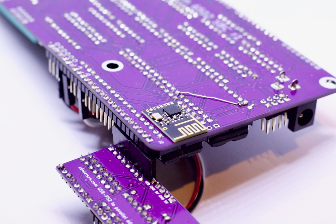
Revision 1 ended up getting a complete rerouting of the PCB, the VGA interface changed a great deal, and the Padauk PMS171B no longer has a place in this project (though I will absolutely find something else to use a 7 cent MCU with ADC and plenty of IO for!).Instead, the only next century tech is the introduction of the nRF24L01+ compatible module neatly tucked away on the back of the board and the 3v3 regulator near the power LED's.
![]()
On Rev0 I was happy with the fact that I could seemingly save a couple of logic IC's for the price of 7 cents for a PMS171b, but the frustration of not being able to set the counting outputs to high impedance mode and hence the necessity for two more 74HC245 bus tranceivers just drove me crazy along with the fact that I was using two 4 bit counters for the remaining 8 bits.
Well - just remove the PMS171B, replace the counting logic with two 74HC590 8 bit counters instead and some glue logic for the sync signals, right? Right? No... That wasn't enough.---------- more ----------Even though I could connect the counter lines straight to the RAM address lines because I have connected the ~OE line of the '590's to phi2(meaning the counters are only driving the lines while phi2 is LOW and the CPU isn't using the busses) to prevent bus contention, the glue logic I had planned to decode the VSYNC and HSYNC signals was completely messed up - the signals were triggering all over the place because they were also triggered during PHI2 HIGH.. Auch.. Maybe there was no way to avoid the two '245's?
It turns out it wasn't that hard after thinking through it all a few nights. First I tried to make do with an SR latch - no dice. Then a 74'74 - no luck either. Finally the 74hc109 JnotK flip flop to the rescue, only allowing the sync signals to change in the correct direction, when phi0 goes high(which is a bit before phi2 goes high). Even better - the jailbars I had seen on the display were a thing of the past, indicating this was an even better solution.You might also notice the LED's around the '273 register on the board has funny names - that's another significant upgrade from r0.
...to be continued.
Here: https://hackaday.io/project/184725/log/204739-so-what-else-is-new
 Anders Nielsen


