-
Have you met the 65uino?
03/27/2023 at 18:21 • 0 commentsThank you all for your support in last year's Hackaday Prize!
This year I went back to the drawing board and thought: How can I make a project a bit like my #ABN6502 SBC R1 but even more accessible to students, teachers and hobbyist and make a board that's quick to make and easy to understand?
The answer is my new project for this year's hackaday prize: The #65uino !
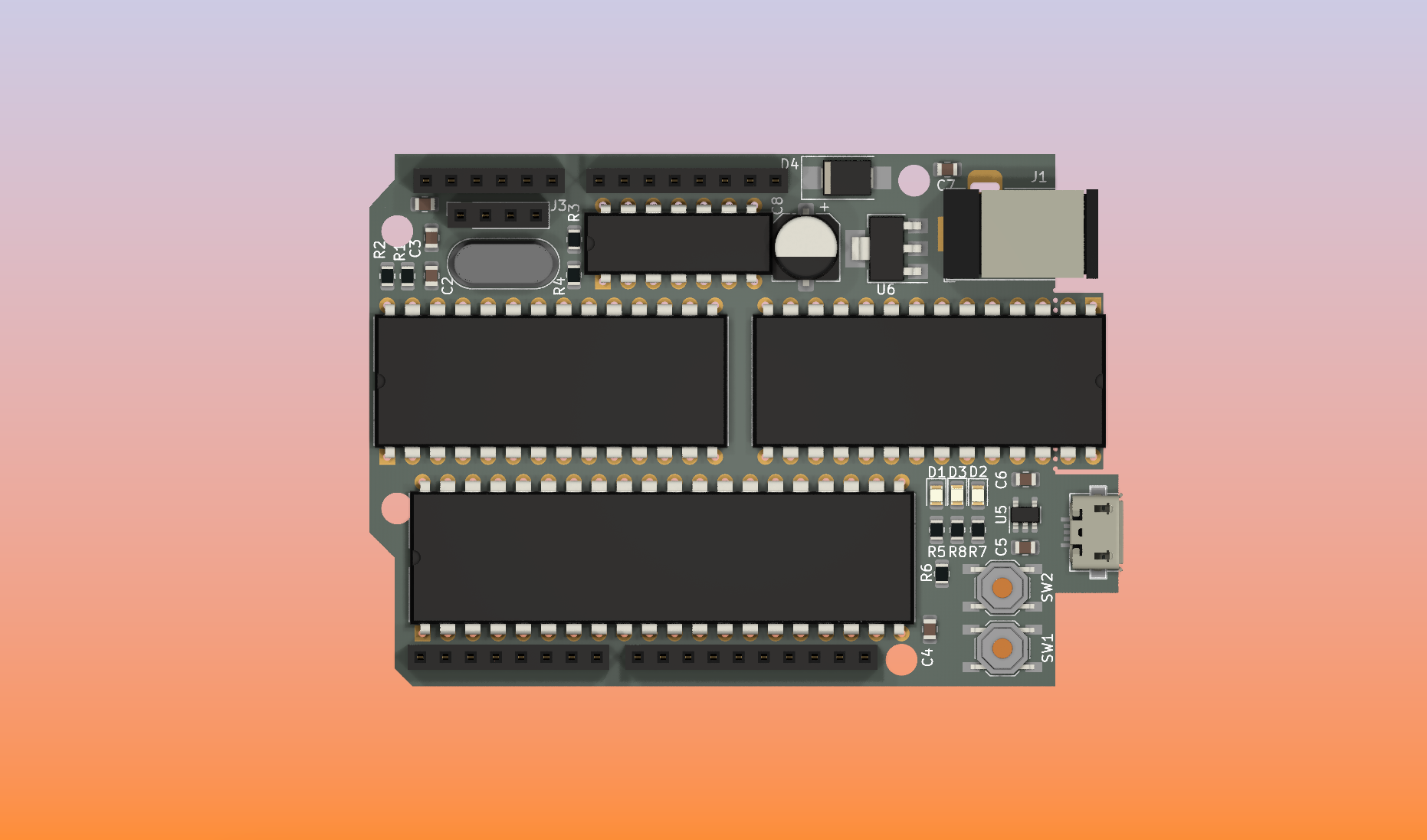
It's a 6507 based dev board inspired by my "6502 Single Breadboard Computer" in an Arduino form factor with only three main IC's + glue and regulators.
It's fast to assemble and it should turn out to be a fun project for students, teachers or a hobbyist weekend project!I hope you'll check out the project and follow along on the main page, here: #65uino
-
Hobby friendly gerbers available!
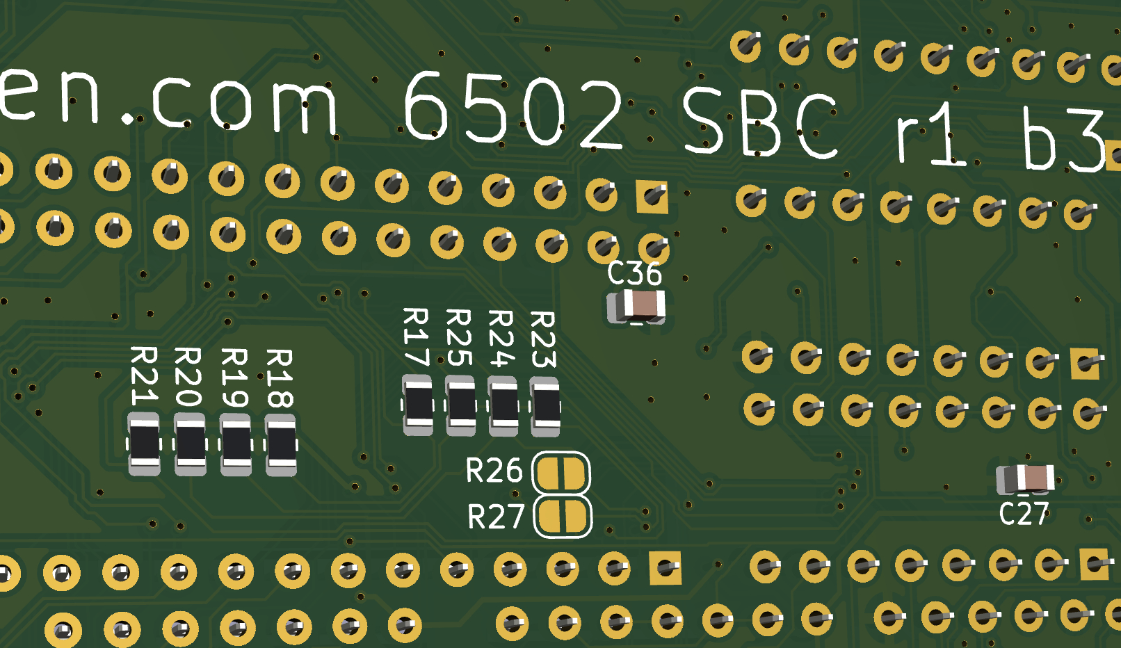
11/24/2022 at 22:28 • 0 commentsTurns out 0402 pads for solder jumpers are a bad idea. They are now a much more friendly size and the board should now be easy to solder for anyone comfortable with 0805 pads. (Not counting the optional microusb connector, the 3v3 sot23 regulator and the castellated hole pad RF module module).
Speaking of 0805 pads, I've added a bunch of redundant 0805 decoupling capacitor pads on the back of the PCB. On the schematic they're marked as "NC"/No Connect but if you're not comfortable with the 0603 100nF capacitors on the front of the board, throwing 100nF caps on these 0805 pads should be sufficient decoupling, assuming a decent power supply.
And finally, speaking of power supply, J1 and J8(0.1" headers) can both be used to power the board in case you don't solder a microUSB connector to the board. They now come with 5V/GND labels - the board has no reverse polarity protection, so do be careful not to plug power in backwards.
I haven't shipped this build to a fab yet so please let me know if you do - nothing critical has really changed since R1 B2 but please regard it as UNTESTED until I remove that label from the gerber zip filename.
The updated gerber zip can be found in the hardware folder on github: https://github.com/AndersBNielsen/abn6502
-
The fun has just begun!
11/06/2022 at 11:14 • 0 commentsThe project might not have finished top5 in this year's Hackaday Prize but I still have to thank everyone here, and Hackaday staff, for all the support - and a big congratulations to the winners!
Even though the 2022 HaD Prize is over the project certainly isn't going on the shelf - it has a permanent place on my desk as a helpful gadget that let's me easily do tons of tasks.
Testing a logic IC is as simple as connecting it to port A and reading it, and testing old parallel equipment is super easy with the address, data, and control lines broken out. I'm sure it'll be featured in a couple more videos on my youtube channel.
In the coming week I hope to update the board slightly as I might have underestimated the size of the random hacker's soldering iron tip - 0402 solder jumper pads will be no more, and changed to actual solder jumpers of a more reasonable size, a minimum amount of decoupling caps will be changed from 0603's to 0805's where possible, and that should make it slightly more hacker friendly.
I probably won't order the new design next week though so if you decide to try it out before I do then please let me know.
Since I don't plan on making the ROM in circuit programmable any time soon, I also plan to move the control register into ROM address space since the register is write only anyway and the ROM is read only anyway. Not happening this week though, so after I make the "user friendlyness" changes this week might be a good time for you to make one.
If you missed the RIOT video, check out what I use my SBC for.
-
New build, new video, updated documentation!
10/22/2022 at 18:35 • 0 commentsAs you might have noticed I recently uploaded my official contest video to Youtube. If you haven't seen it, it's embedded a bit further below.
If you've been following along you might notice that the barrel jack connector has mysteriously disappeared and has seemingly been replaced by a USB-connector. The explanation here is that I did manage to squeeze in the 74hc74 flip flop onto the board to have the PS/2 keyboard connecting straight to the board without a daughterboard - a nice trade for a barrel jack. In return two pairs of 5V+GND 0.1" headers have been added - J1 and J8.
At the same time I also managed to squeeze in another 74HC00 NAND IC, which let me fix the control register decoding - it now only listens on write cycles and has been moved to $7000, which means more RAM freely accessible. This has also been fixed in the project details.For this build I also managed to make the address space from $4000 to $5FFF jumper selectable - which means it's easier to switch between using it as RAM or IO space, shorting either R26 for RAM or R27 for making it floating address space.
The character ROM also got another address line enabled which means each "bank" now has 256 characters instead of 128 - that should make it easier to fit some PETSCII pixel art characters in there without switching banks.
Lastly I've added a bunch of 0402 jumper pads which understandably scared a newcomer away from ordering a board - for now they are intended as a test/debugging way of skipping the 74HC245's as I suspect they might not be needed when using a 'C02 since it also has the BE pin which should do the same and float the address bus.
I did manage to need one bodge since I also removed the unnecessary phi2 buffering but forgot to connect Ø2B and PHI0 (Aka 2MHz) - super easy fix and already fixed in the gerbers.
I regret moving some of the pinheader jumpers to 0402 pads, since 0402 pads are surprisingly resistant to being solder bridged - I will absolutely find a better footprint for the solder bridge jumpers before I order more PCB's.
From the Youtube comments I also learned that 0603 capacitors might also be on the small side for most interested people - so I might up that to 0805's as well. It really is meant to be solderable by a hobbyist with a relatively huge soldering iron - though power supply might have to be via pin header now that the barrel jack is out of the picture.So, is this a new "revision"? Meh - I've decided it's merely a new "build" as most of these changes were always intended to be part of R1 and most of the routing and general idea remains the same. So say hello to the ABN6502 SBC R1 B2 - now with a USB port for PS/2 keyboards.
Thanks for the support to everyone so far!
-
Using my #ABN6502 SBC R1 to test RIOTS
10/12/2022 at 07:30 • 0 commentsWhen I'm talking to my friends it's not always easy to explain why I would put together a computer out of 40-50 year old parts, but besides having fun with it, it really does have a lot of practical value.
Since it's sitting there on my desk anywayy - with control signals neatly broken out, 5V and 3v3 available, along with the complete 16 bit address bus, data bus and plenty of IO - it really does beat a Raspberry Pi or an Arduino for easy of use.Flip the power switch, turn on the screen and use the keyboard to scroll through memory or scan for I2C devices - it really doesn't get much easier than that.
If it's hard to picture, I made a quick video yesterday that shows how I do just that.
P.S. Contest video about my 6502 SBC coming soon!
-
WHUUUT! It runs BASIC?
09/19/2022 at 22:12 • 0 commentsIt's not exactly Crysis.. It's not even DOOM.. But for the real retro crowd BASIC certainly seems to be the true test of a real 1970's microcomputer.
And now mine does it too!
I somehow managed to mess up the memory map configuration when I first tried to get it running and that certainly delay'ed the whole thing a bit(yes, I spent more time than I care to admit), but after learning a lot about cc65 macros and how Bill Gates and Ric Weiland architected their version of BASIC from the experience, it was smooth sailing from there - I even managed to quickly write up some wrappers for saving to and loading from tape! Proudly featuring my #Simple Universal Modem !
I hope the video will be well received. Either way, I had a lot of fun getting to this point - next stop: I2C-land!
-
This project spawned a new one!
07/21/2022 at 09:27 • 0 commentsHello everyone!
These last couple of weeks I've spent a bunch of time recording data to my 1972 tape deck. I couldn't decide if it was a part of this project or it deserved it's own project, but went with a new project since it's very self contained and applied much broader than just a single 6502 computer.I suggest you check out the daughter project here on hackaday.io - the Simple Universal Modem - here: https://hackaday.io/project/186309-simple-universal-modem
I've already made a video demo, so check that out too:
-
Thank you for the support! What's next?
06/07/2022 at 09:56 • 0 commentsI'm overwhelmed with all the positive responses to my new hardware overview video. Thank you all!
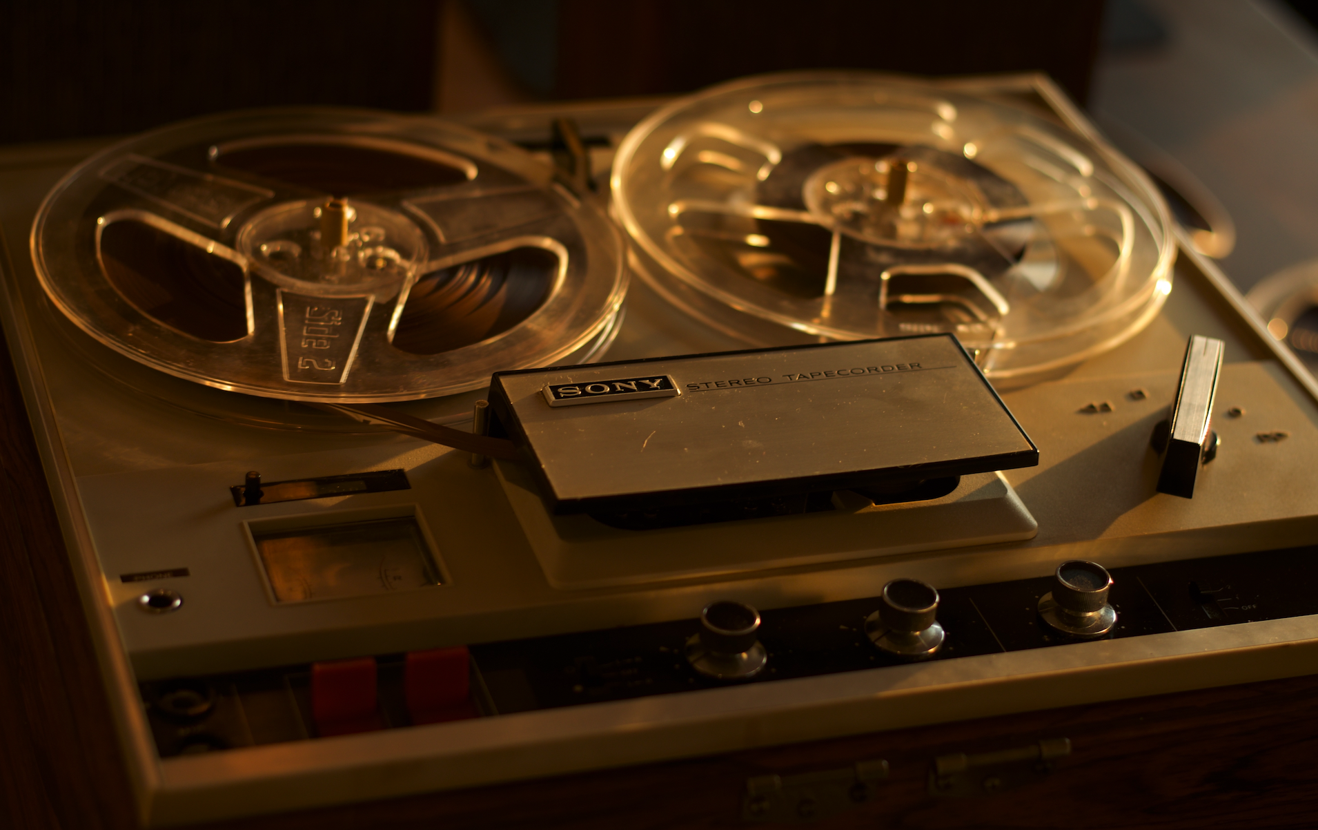
In the near term I'm focusing my efforts on making a tape deck interface, letting me save data on reel to reel tape - the way I'm sure Chuck Peddle intended it! :D The big question here is if I can make something that will make sense as a permanent part of the SBC, or an audio data interface will remain an external add-on.
Of course this wouldn't be limited to 1970's tape but should work fine with the audio jack on your modern laptop. I'll have to test both.
When that's done I will probably focus my efforts on porting one of the MS Basic versions - I'm sure it'll be glorious!
When that's running I might decide to grab an old laptop screen and see if I can make the world's - probably - first 6502 cyberdeck!
![]()
-
Complete hardware overview video out!
05/27/2022 at 16:23 • 0 comments -
New video coming soon-ish!
05/16/2022 at 21:02 • 0 commentsAs I've been promising for months, I will eventually release a video about all the hardware of my 6502 single board computer - not just the changes since r0 but the whole thing.
I plan to go through all the major hardware components in about a half hour long video - beginner topics will receive less attention than the things that make this single board computer unique.
At the very least the topics covered will be:- So what is a “6502”?
- Memory mapped IO
- A memory map from half a century ago
- SPI, I²C, and PS/2
- Reset and buffering circuit
- “VGA” output
If there's anything else you would like me to explain in the video, now is the time to leave a comment :)
 Anders Nielsen

