This is another log I moved out of the quick comments because it's starting to snowball.
For a point of reference, the resistivity of pure/bulk metals are approx:
- Copper: 2 μΩ cm
- Brass: 4 μΩ cm
- Iron: 10 μΩ cm
- Stainless: 90 μΩ cm
Finding "Copper Composites and Laser Sintering: Novel Hybridization Method for 3D Printed Electronics"
On April the 24th, I found this open-access paper that's 2 years old:
Two notable quotes are below:
PLA-based composites with 90% and 80% (wt.%) copper loading [with] a 5.5-W 450-nm blue laser with various combinations of parameters to “sinter” the surface of the samples. [...] The copper particles became oxidized during the process, and none of the samples yielded a conductive result.
Instead of partial melting, sintering (i.e., bridging adjacent particles) can be achieved by chemical reaction that causes deposition of a native copper layer on copper particles [...] using copper formate, which [...] spontaneously decomposes at approximately 200 °C to form native copper and volatile compounds. [...] However, copper formate, formic acid, and ethylene glycol are all incompatible with the temperatures associated with FDM printing (200–250 °C).
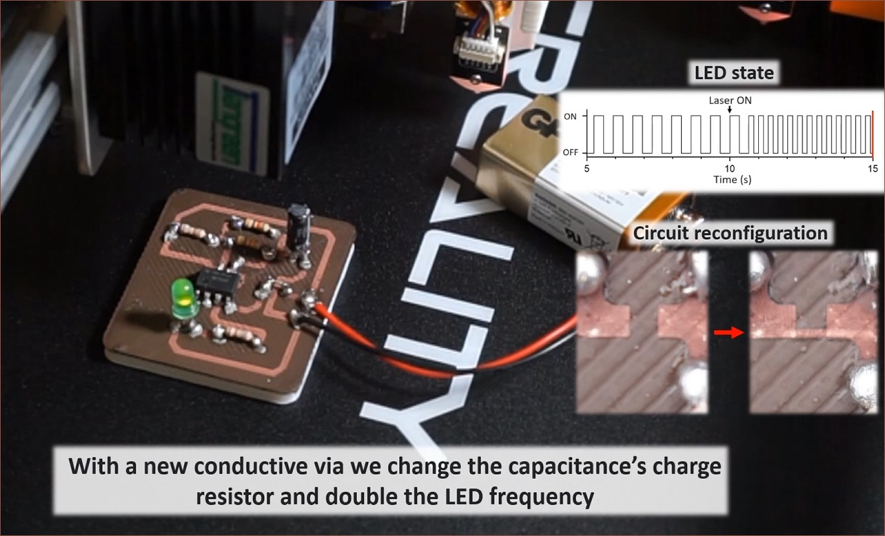
They reported a resistivity of 400 μΩ cm and included a video showing a 5.5W blue laser adding a new trace to a printed, active circuit:
![]() Finding loads more papers
Finding loads more papers
Because I don't have the limitation of FDM, and my hypothesis of sintering particles suspended in matrix possibly disproven, I started looking into what the aforementioned paper was talking about when they mentioned native copper formation.
It seems that it's possible to use a laser to "reduce" copper (oxide) nanoparticles to copper at a temperature low enough to apply circuits onto PET, for example. General reading gives the impression that copper oxide nanoparticles are more stable than copper nanoparticles.
- One-Step Fabrication of Copper Electrode by Laser-Induced Direct Local Reduction and Agglomeration of Copper Oxide Nanoparticle (2011)
- 31 μΩ cm
- Laser: 1070nm 0.4W 25μm at 30mm/s
- "There are two types of copper oxides: CuO and Cu2O. The band gap of CuO (∼1.2 eV) is lower than that of Cu2O (∼2.1 eV). Hence, Cu2O is reported to have a high transparency with a slightly yellowish color and usually absorbs wavelengths below 600 nm, while CuO strongly absorbs the whole visible spectrum range and is black in appearance."
- So it sounds like a 450nm laser should be fine. I expect all the researchers are using lasers that their uni had on hand, and high powered blue lasers are relatively new.
- Photonic Sintering of Composite Pastes with Copper Oxide Powders Using Different Light Sources (2021)
- 8 μΩ cm on PET substrate
- It seems only a single layer is formed in these experiments, so the substrate its on affects the resistance.
- Laser: 638nm 1W
- 8 μΩ cm on PET substrate
- Direct Writing of Semiconducting and Conducting Microstructures by Using Selective Laser Sintering and Reduction of CuO Nanoparticles (2024)
- 88 μΩ cm
- Femtosecond Laser: 800nm 0.04W at 0.004mm/s
- "The cupric oxide (CuO) nanoparticles are air stable, cheap, and easily available materials; they are also good precursors for fabrication of Cu micro/nanostructures by using selective laser reduction."
- So I guess this is why they're common in academia.
- Fabrication of Flexible Copper Microelectrodes Using Laser Direct Writing for Sensing Applications (2024)
- 62 μΩ cm
- Laser: 1064nm 0.955W* at 60mm/s
- *This laser was defocused because it's minimum power was 10W for a 42μm spot size was too much.
- Direct laser writing of copper and copper oxide structures on plastic substrates for memristor devices (2023)
- They only mentioned ohm/square measurements
- Laser: 1064nm 4W 15mm/s
- Additive Manufacturing of Electrically Conductive Multi-Layered Nanocopper in an Air Environment (2024)
- 28 μΩ cm
- Laser: 1064nm 2.5W 50μm at 150mm/s
 kelvinA
 Finding loads more papers
Discussions
Become a Hackaday.io Member
Create an account to leave a comment. Already have an account? Log In.