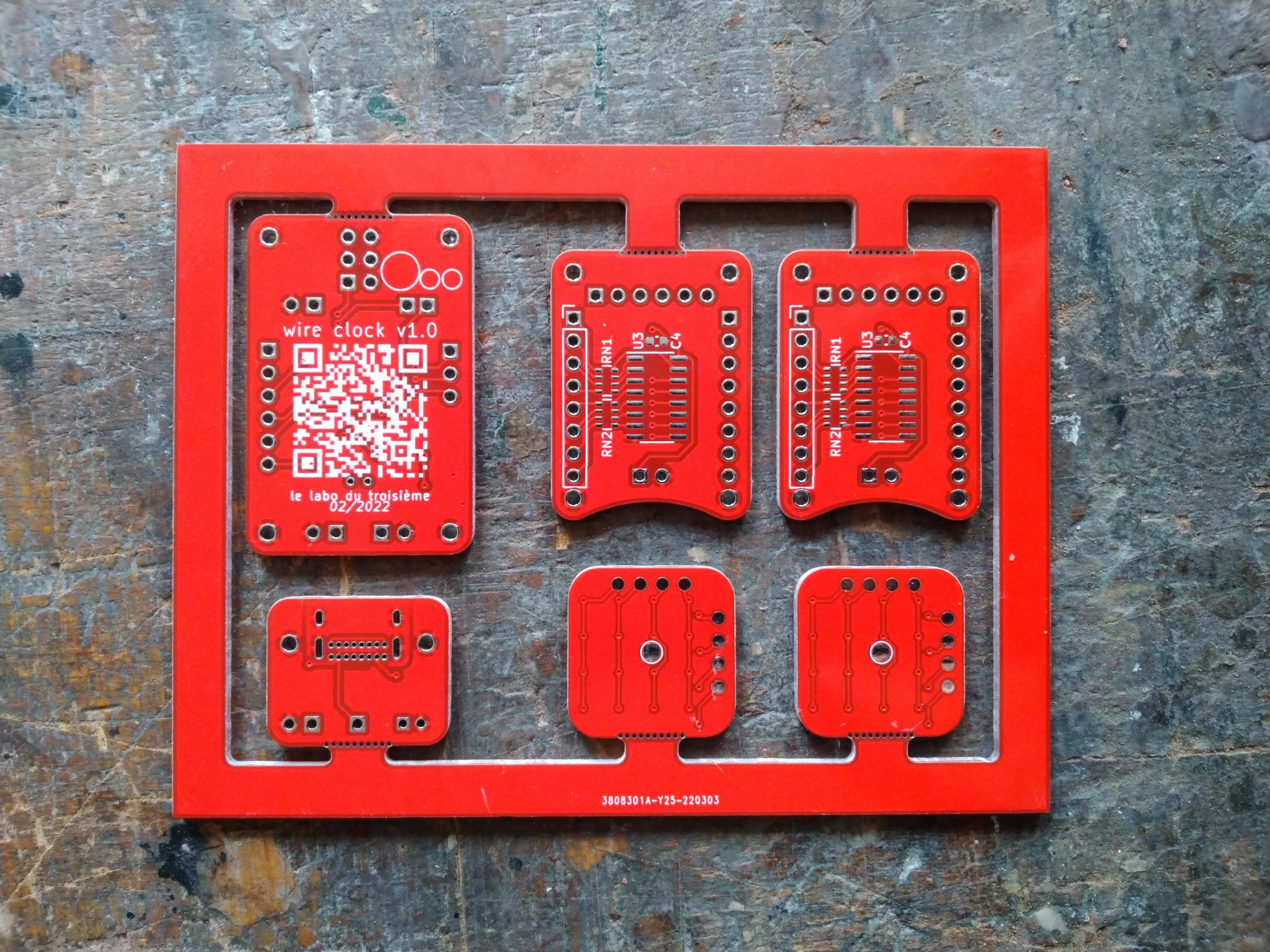
It's been a long time since I wanted to give a try at freeform circuits (or circuit sculpture, call them how you like). And preferably a clock, because it's probably the most obvious thing can be useful in everyday life. In fact, the clock should have an old calculator VFD display. The ones I saved here and there will one day come to life again.
So. Clock, freeform. Freeform, but there's a catch : I'm quite lazy. Planning something too complex was the best way to start nothing at all. And a display, two shift register, a microcontroller, quartz, photodiode and amplification circuit, plus a safety cell start to be something complex, at least if every connection has to be hand made, and hand shaped. That's roughly 120 wires to cut, form, etc. Plus, I love the esthetic of PCBs. Making a PCB that groups functions on several individual boards could be a good base for several different geometries, and that will easy the freeform assembly.


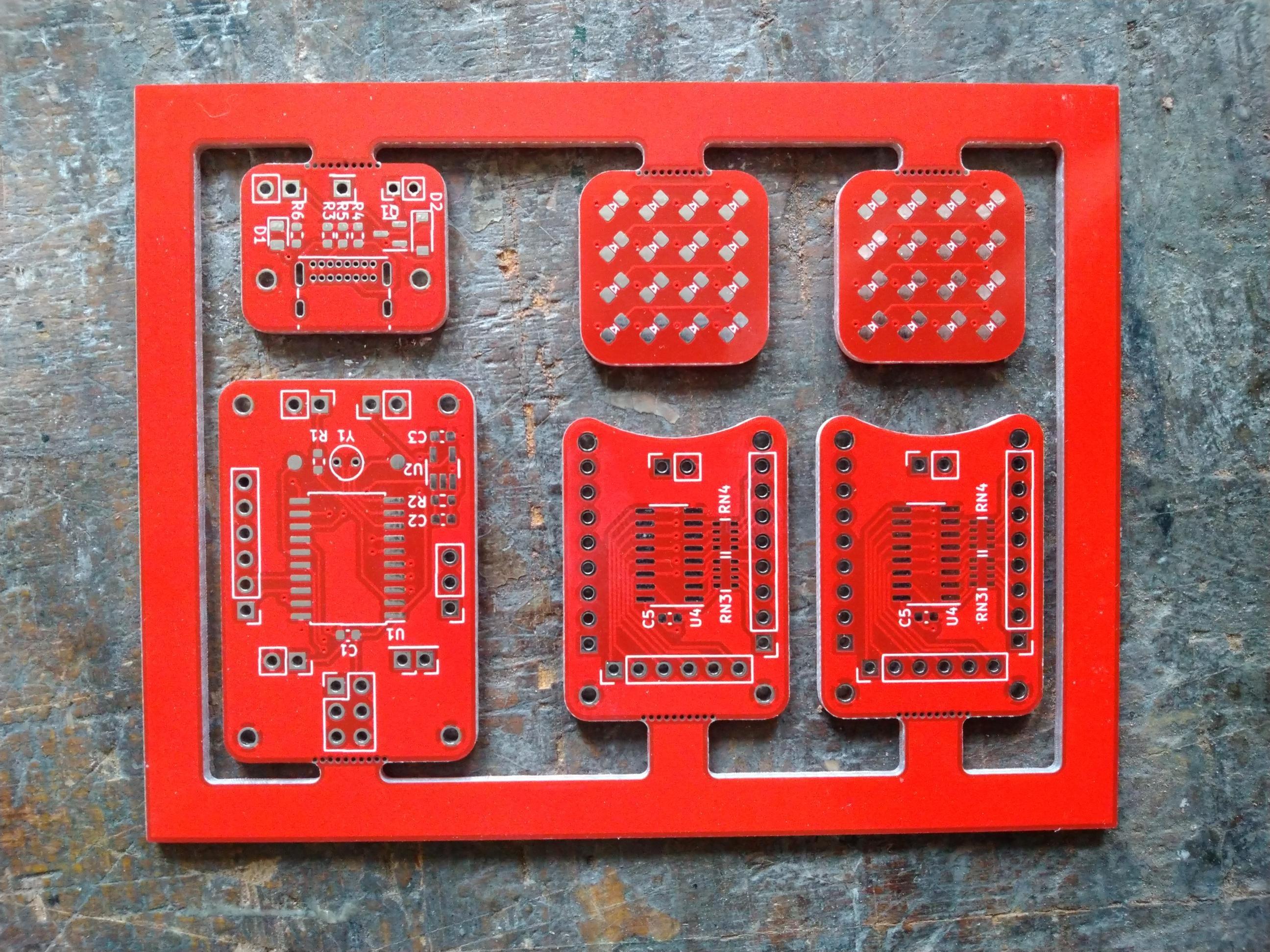
The circuit has been subdivided in three (four) different circuits :
- Main board. This contains the Attiny 816. Side note : I was planning to used an Attiny 1616 instead, but you've maybe heard of ship shortage ? That's this thing that makes you design a board not following the functions you need, but what you can source before two years have past. Seriously, for some projects I work on, we had to revise the design not to correct bugs, but to accomodate for different references or footprints that are available...
Attiny 816, connectors to other boards, crystal (dedicated log to come), photodiode and its amplification circuit. There is also a UPDI port for programing, and while I've followed Microchip recommendations for this footprint, I should not have. On next revision I'll use the three pin connector recommended by SpenceKonde of MegaTinyCore (which is the Arduino plugin used for programming the Attiny series 1). The three pins have two advantages : less real estate used, and it's symmetrical, so can be used from both faces. And I quickly realized that it's not useful : it's essential, given how constrained space can become on this kind of project. :D
There are three connections for buttons, to set time. I didn't know while designing PCB what would be those buttons, so I just provisioned ports. They could be capacitive buttons, classic tact buttons, or freeform. After all, a button is a device that shorts a circuit, so let's be creative ! On future revision I'll probably add a button board : I don't like capacitive that much (mostly because I prefer the tactile feedback of a button), and "wire buttons" do not inspire confidence. - Power board. Quite straightforward. A USB port. It's the first time I use USB C connector. They are available in a wide variety, from completely implemented USB C to power only, with USB 2 in between. On this board there is a power led, a provision for connecting a coin cell for data saving in case of power loss, and a few resistors (USB C asks that you place pull-down resistors on CC1 & CC2 lines when replacing USB B or micro B).
- Shift register boards. There are two of them. One is used for providing VCC to each segment, the other to provide GND connection for active digit. The SR can be mounted on either side of the board, the output ports are symmetrical. The idea is that two boards can face one another, the inputs pins are aligned (except of course the data pin, as they are chained), and each output pin face a non-connected pin on the other board. That way the two boards form a strong assembly with 16 wires forming two 8 bits "data bus", going from their pins on one board, to "mechanical" pins on the other. And following how we want to place things in space, SR can be mounted to either face.
The drawback of this is that the boards virtually becomes a "two-sided one-side PCB", as there is no room for vias. At least on the size I wanted not to exceed. It contrains the port to map the SR pins one on one. Initially the connection were supposed to match with the main board. That's no longer the case, but that adds a bit of intricacy to the wires. - Lastly, there are two little square board. I'm always sad (kind of) to have some resources not used. That's the case here : with a 4 digit display, there's only half the outputs of the shift register used. I wondered what I could do with the remaining, imagined 32 leds bargraph (that I even designed in Kicad), or two 16 leds bargraphs, before I realized that 16 is 4x4, and settled for two 4x4 matrix. That end up not beeing used, as you can see.
A final note : I would never have designed such a circuit made of several different boards without a fantastic tools, Kikit. It makes panelizing almost as easy as blinking an eye. It's been mentioned on Hackaday, and you can find the reference here. I really owe Kikit to have unleash the potential of what can be made with PCB.
 Pierre-Loup M.
Discussions
Become a Hackaday.io Member
Create an account to leave a comment. Already have an account? Log In.