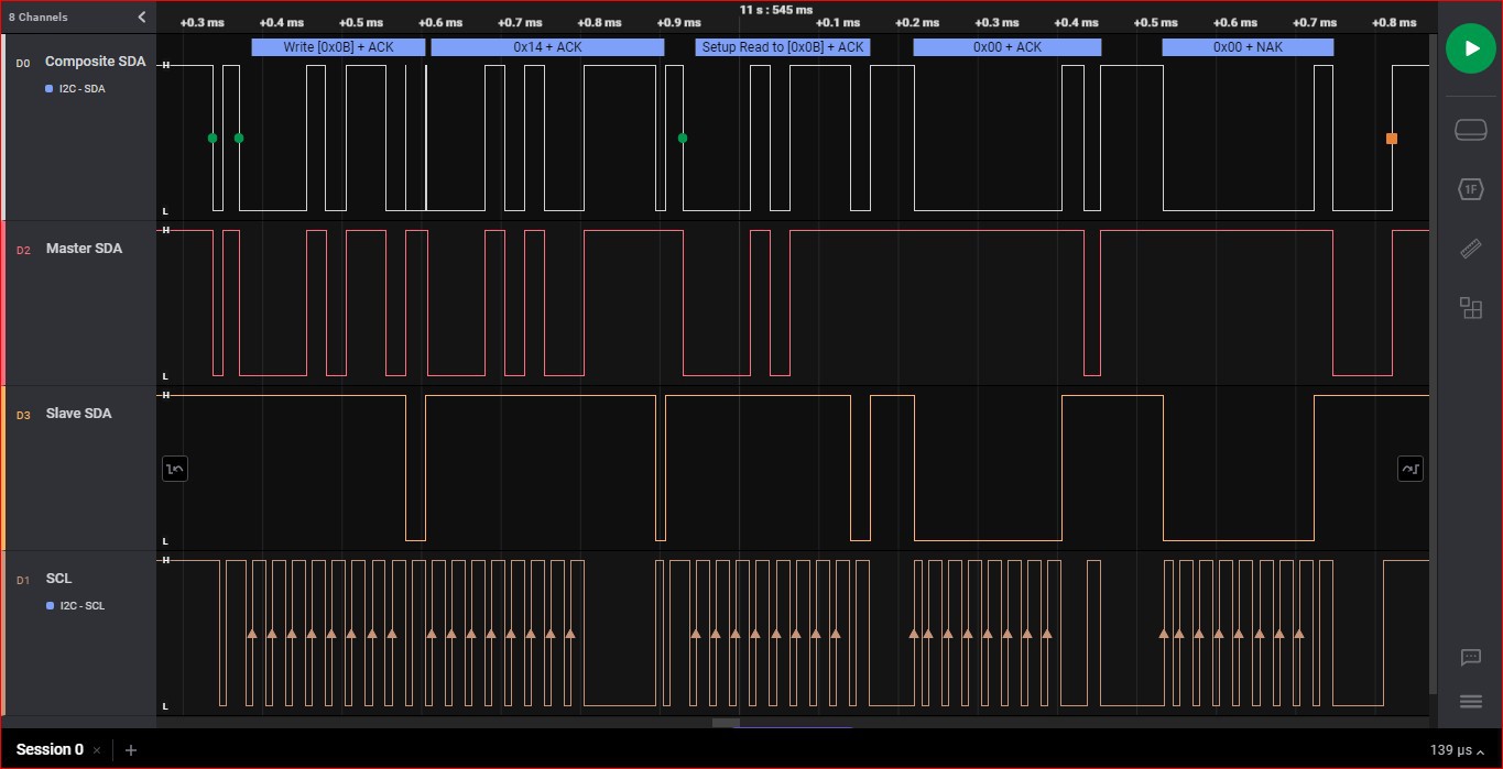
4 Channel Data Analyser screen dump.
From top to bottom:
Composite SDA
Master SDA
Slave SDA.
SCL.

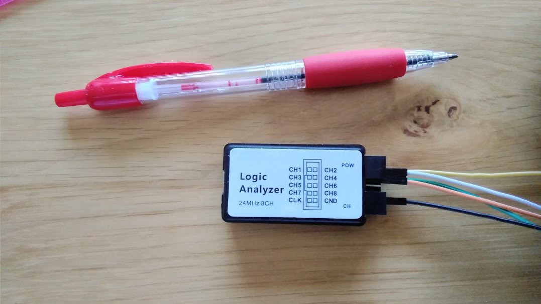
Logic Analyser
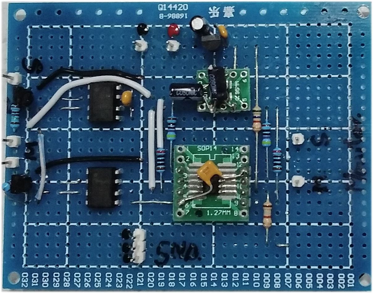
Rough and ready test PCB

This project is ideal for learning about the I2C protocol if you're new to it, because you can clearly see each and every transition and who's doing the transitioning.
Normally it is only possible to monitor the composite SDA line which carries both master and slave data, so it's hard to know who is sending the ACK pulses or who is holding the line low or answer the question: 'What are those narrow pulses all about' ? etc. etc.
By using a cheap multi channel data analyser ex AliExpress, plus this project, you can view all 4 channels ie. Composite Master/Slave SDA line, Separate Master line, Separate Slave line and SCL line on your PC with the free Saleae Logic 2 software. Download from www.saleae.com
A quick search of Aliexpress "USB Logic Analyzer 24MHz" will bring up plenty of units under US$10 incl shipping.
This project is a bit 'rough and ready' The schematic is hand drawn and there is no PCB artwork or .pcb files supplied. This is more than made up for by the detailed info supplied in this text.
It is designed so you can knock a board out with spare parts you may have lying around.
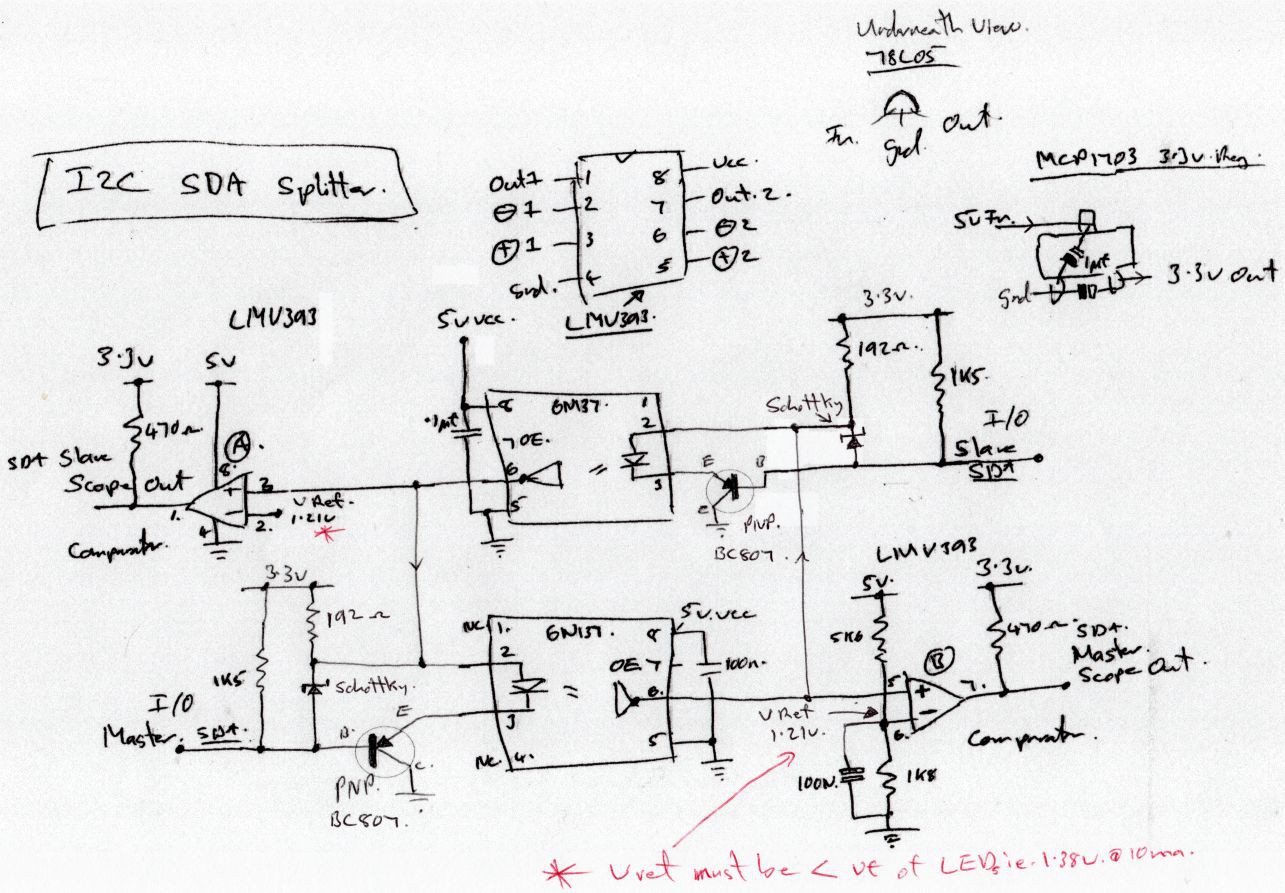
Circuit Diagram:

Desciption of Circuit :
I won't describe the isolation circuitry in full as it's a standard arrangement, better described by the likes of TI etc.
The two signals on lines labelled I/O Master SDA and I/O Slave SDA are separated with a standard dual opto coupler arrangement. I used the 6N137 ICs here due to their much faster switching times than their 6N138 or 139 cousins. 138 and 139 versions require 1K5 base bias resistors at 100Khz, between pin 7 and ground also. Pin 7 of the 6N137 has a different purpose and is an output enable pin. Pulled high internally, you can leave it open circuit. You can use any fast optos here though if you want to.
In addition to the standard I2C isolation arrangement circuitry sourced from TI's app notes, I've added two comparator gates which enable the Master signal and Slave signal to be filtered and output separately.
These comparators will only switch low when their associated 6N137's LED is active. ie. when 6N137's pin 6 is at GND level which is below the 1.21 volt comparator threshold.
The 1.21 volt comparator threshold, filters out the 1.38 volt LED Vf signal which is produced when the other non associated 6N137's LED is activated.
1.21 Volt comparator threshold was chosen due to the fact I had some 5K6 and 1K8 resistors available.
Any Vref between 1.38 LED Vf and pin 6 of 6N137 GND voltage will suffice.
___________________________________________________________
The comparators' pins 3 & 5 get to see 3.3v, 1.38v or GND levels depending on who's doing the switching.
A low going signal input to I/O Slave SDA will never reach pin 7 of Master comparator because its pin 5 input will see 1.38 LED voltage which is still above the 1.21 V threshold. The same applies to the duplicate I/O Master SDA circuit.
The Composite SDA signal line to the data analyser can be taken from either I/O Master SDA or I/O Slave SDA. They both see the same signal after all, separated only by the circuit's propogation delay.
The SCL lines wire directly between Master and Slave devices because the master alone (under most circumstances) has control of this line. The I2C spec does allow for the Slave to take control of this line under special circumstances, but I've never come across it. You could, however, have a duplicate circuit arrangement for SCL lines if you so choose. It's up to you.
NB: 6N137 optos and LMV393 comparators are powered with 5 volts for faster switching times than would be had from 3.3 volt supply. All 4 outputs are open collector devices connected to 3.3V rail via their respective pull up resistors.
BC807 PNP devices (or just about any PNP type ) are wired as emitter followers for Hi to Low impedance conversion purposes. We actually want close to our 10ma LED current if we can get it. Without the transistors we'd have to rely on our Master and Slave devices to sink this current for us, which from memory would be out of I2C spec.
Don't forget the common GND wiring for the Master and Slave devices and Data Analyser also.
5 volt supply can come via a battery and simple 78L05 regulator or a 5 volt cellphone charger even. Not clearly obvious on the schematic, but 5V reg output also connects to input pin of the 3.3V regulator.
There are bound to be better ways of doing this job, like with the newer digital isolation chips or maybe a single microcontroller and a dozen lines of ASM code, which I may yet have a look at. Nevertheless, I can't find anyone online who has done this using any method at all. It is such a great I2C learning tool too.
Anyway, opto couplers lend themselves ideally to this task with their LED forward and reverse biasing attributes used in the isolation circuitry. Note the compulsory use of schottky diodes here. They cannot be regular old diodes with high Vf spec or the circuit may not work.
The 192 ohm resistors are the values chosen that would allow 10ma to flow at 1.38 Vf through the 6N137 LEDs with 3.3V supply ( ignoring any voltage drop accross BC807). The next highest available value ie. 200 or 220 ohm will do the job fine.
Important:
The cheap data analysers ex AliExpress don't seem to work well at all above 8Mhz sample rate. In fact, setting them higher seems to decrease the sample rate.
The main MCU chip is an Infinion Tech CY7C68013A-56
Perhaps someone reading this may have an answer to this.
If you have any questions at all, please ask.
