Close
0%
0%

Discrete Geiger Counter V2

Portable, low-power geiger counter made exclusively from discrete components

Public Chat
Similar projects worth following

Project Goals

As a amateur mineral collector, I was recently in the market for a portable geiger counter to locate radioactive minerals. There are dozens of off the shelf geiger counters and kits that would work just fine, but they either seemed too expensive or too boring looking (the most important metric). Of course, this is the perfect reason to throw practicality out the window and make one from scratch. Before getting into the design, I made a list of boxes this geiger counter had to check. 

  • Portable, ideally pocket sized
  • Low power operation from commonly available batteries
  • Reasonably sensitive to background radiation
  • Discrete component design for a bit of a challenge

Version 2 Design files ***unverified 8/9/24***

I'm still in the process of building this version, so the design files are untested as of yet. The BOM file details everything needed to make this geiger counter except for consumables. Most electronic components have an alternate non-automotive substitute that can be used instead if the primary part # is out of stock, or if you want to save a little cash. I had the PCBs and 3D prints done by JLCPCB, but feel free to use other fabs if you prefer.

Schematic

LTspice simulation

BOM

AEC-Q Digikey cart

Budget Digikey cart

Mainboard gerbers

Battery board gerbers

Component Placement

3D Models

Schematic.png

Portable Network Graphics (PNG) - 522.33 kB - 08/09/2024 at 18:20

Preview

bom.xlsx

sheet - 11.69 kB - 08/09/2024 at 18:18

Download

Placement.pdf

Adobe Portable Document Format - 39.98 kB - 08/09/2024 at 18:16

Preview

Cutaway.PNG

Portable Network Graphics (PNG) - 94.37 kB - 08/09/2024 at 16:41

Preview

Discrete Geiger Counter v2.pdf

Adobe Portable Document Format - 128.09 kB - 08/09/2024 at 16:04

Preview

View all 12 files

  • Mechanical Overview

    Caleb W.08/09/2024 at 14:56 0 comments

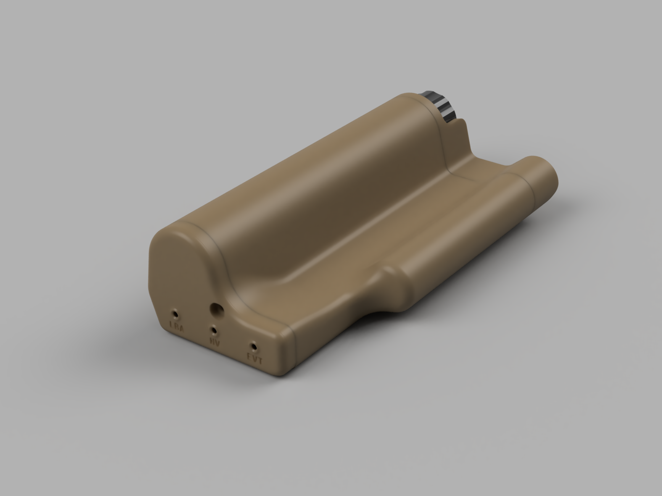
    In this entry I'll go over the mechanical considerations for the project. This is probably the most detailed drafting I've done so this part took a lot longer than it should have. There are some things I would change in future versions, but what I have currently should get the job done.

    After a lot of thinking, moving the battery positive terminal to a daughterboard along with the indicator LEDs made the most sense. This uses spring loaded connectors which make contact the main PCB. The battery cover has a recess to accept the daughterboard, which will be potted in place with epoxy. This is then covered by a faceplate which also gets glued on. Since I'd like this design to be rain resistant I made two grooves for orings where the battery cap slides into the main housing. This is where most of my design uncertainty lies, because it's really pushing the limits of current 3D printing technology for these to work as expected. Hopefully I left enough room to not shred the orings after repeated use without compromising the seal. The tolerances are very tight around the oring seals, and this may end up causing waterproofing issues. I'll probably beef up these areas if I decide to make subsequent housing versions.

    On the bottom side of the main housing is a circular hole for the piezo element to be glued in. The piezo element will also be attached to the PCB by jumper wires. I have had good success from JLCPCB for previous projects, so I'll be trying out their 3d print service for the first time. I'm not sure what level of accuracy I can expect, so in addition to MJF I also ordered some SLA parts in CBY resin.

    I would preferred screw-oring seals instead of gluing to make disassembly possible, but I decided to abandon this idea at least for the current iteration. Designing in oring grooves and screw holes take up a lot more volume than glued connections, and I didn't want to spend a lot of hours on this quite yet. So for now I plan on gluing the pieces together with DP8910NS made by 3M, which is a 2 part acrylic adhesive specifically designed for nylon. I was able to find a 45ml tube on Amazon for $20, but elsewhere it was very pricey. Plastics are notoriously difficult to bond due to their low surface energy when compared to metal or glass. There are ways to increase the surface energy via flame or plasma treatment, which I have had mediocre success with. My extremely limited plasma treatment setup involved running a portable ozone generator inside an enclosed container for a few hours. While not technically the same as real plasma surface treatment, my theory is that the ozone should be able to micro-etch the surface of the plastic, making it more receptive to bonding. In practice, I didn't see much difference. I saw virtually no change in treated polypropylene, and only a small improvement for PET. The ozone is clearly doing something however, as both test swatches were bleached white after treatment. Hopefully none of this will be necessary if the DP8910NS performs as expected.

  • Version 2 Redesign!

    Caleb W.07/30/2024 at 19:05 0 comments

    It's been over 2 years since the last project update, but recently I've revisited the design and decided to work on version 2, which should have significant improvements over the first iteration. Again, the purpose of this project is more of an exercise in old-school electrical engineering rather than trying to optimize for the usual metrics such as cost, performance, or simplicity.

    I was happily surprised with the performance of version 1 given that it worked on my first attempt. However there are still a few things I wanted to improve upon:

    1. The power source. CR2032 cells are easy enough to come by but the battery life was sub-optimal, and I ended up using a 9V battery for higher efficiency. AA batteries are much more common and store significantly more energy then the latter two, so I needed to re-design the circuit to work from a low voltage source.
    2. Click volume was very quiet, I'd like the new design to make clicks that are more pronounced.
    3. Version 1 relies on Vbe of the bipolar transistor as the reference, and this causes wild fluctuations in output voltage based on temperature. In extremely cold environments this could cause arcing in the tube, so the new design should have tighter regulation.

    Design Overview

    Powering the circuit from a AA battery makes the design a little more challenging than the previous one. I decided to go with the same oscillator architecture from the previous design, since it worked well, and is able to operate down to 0.7 volts. After getting into the LTspice simulations for only a short time, I realized that a system supply would be necessary in order to achieve the efficiency range I was looking for, especially since the HV boost FET necessitates a minimum drive voltage of around 3.5V. A low voltage FET is used for the boost section of the circuit, so ensure startup from sub-volt supplies. The main oscillator is supplied from this system rail, forming a positive feedback loop. This enables the circuit to run on supplies down to 250mV once bootstrapped. While this feature wasn't part of the design requirements, it's a real plus when operating batteries below their recommended temperature range. The system voltage is regulated via a feedback loop which sends a pulse of current through the boost inductor whenever the supply voltage drops too low. There was a strong tendency for my first attempts of this circuit to soft-drive the boost FET, which resulted in increased switching losses. Eventually I converged on a configuration that's able to make sharp and consistent pulses, and this concept worked well enough to use in the HV feedback loop also.  

    The high voltage supply is driven by the same oscillator as the system voltage regulator, and uses the same 1:100 coupled inductor as the previous design. After re-evaluating diode options, I was able to find an ultrafast diode with a reverse recovery time under 25nS. Finding a fast rectifier is crucial for this stage, since this accounts for a large portion of the switching losses on the high voltage side. I found that additional voltage doubler stages had only a minute effect on overall efficiency, so I stuck with one stage.

    For pulse detection, I'm sticking with cathode-side sensing because it avoids the high voltage capacitors and resistors necessary for anode side sensing. Noise didn't seem to be an issue with the previous version, likely because the connections were fairly short. Pulses from the Geiger tube are fed into 3 bipolar transistors, one of which triggers a one-shot timer for flashing an LED. The other two trigger the piezo driver for audible clicks. I spent several days stuck at dead ends until I arrived at the current piezo driver iteration due to the numerous design constraints I had. All my first ideas revolved around feeding the pulse from the geiger tube to a FET-inductor flyback generator that would create the click. The main problem with this approach is with the volume control. I couldn't find a feasible way of achieving...

    Read more »

  • Version 1 Prototype

    Caleb W.05/13/2022 at 01:05 0 comments

    V1 Schematic Overview 

    Starting on the left side of the schematic, Q7 and Q9 form a classic bistable multivibrator which oscillates at roughly 22kHz. This keeps audible noise to a minimum while prioritizing electrical efficiency. The benefit to this type of oscillator is the relatively fast turn off time of the transistors. I found a good balance of resistor and capacitor combinations that have a fall time under 75nsec, which will maximize the amount of energy extracted from the inductor every cycle. These pulses are fed into Q2 via a high pass filter which limits the current pulses through the inductor to 3uS. This is important to keep the main inductor out of saturation, which will waste energy. Also, if the oscillator gets stuck 'ON' for some reason, there is no risk of dumping current through the main inductor. When Q2 is pulled low, Vbe of Q5 drops below 0.6V, and charge from the main MOSFET gate gets pulled to ground via D3. As soon as Q2 turns off, R9 and Q5 form a voltage follower which turns the MOSFET ON. R6 prevents unwanted oscillations in the gate voltage. 

    When the current is cut off from L1, the inductive EMF kickback is fed through the secondary side which adds the two voltages together. This high voltage spike goes through D1 and begins to charge the main high voltage capacitor. R5 and C5 form a snubber network that technically isn't needed, but without it, there is a lot of ringing on the FET drain which will cause a lot of unnecessary RF noise. The efficiency hit is pretty minimal, and it's the 'right' thing to do. The voltage across C1 is sensed via a resistor divider network consisting of R2, R3, R4, and R7. 100Meg resistors are needed here so the leakage is minimal. At 400V, even a 10Meg divider will be the main loss of power in this circuit. 100Meg resistors are a decent balance between leakage current and cost. 

    When the voltage at the base of Q3 reaches the setpoint of 0.7 volts, it begins to conduct. The setpoint voltage can be adjusted via VR1. This lets you use a 100k adjustment pot, which is easier than trying to find a 10Meg pot. A crude voltage regulator consisting of R19, D6, and C12 provides a relatively stable 3.6V for a consistent output voltage across the entire battery discharge range.  The collector current in Q3 is amplified by Q4, and inverted by feeding the collector current from Q4 into Q8 and Q10. Even the tiniest base current into Q8 pulls the gate of Q6 low, cutting power to the oscillator circuit. This lets the high voltage capacitor slowly discharge through the resistor divider. As soon as the high voltage line drops slightly, Q6 will turn the oscillator back on, forming a negative feedback loop. Very high loop gain is preferable, as it improves load regulation and response to transient current draw from the geiger tube. R17 and C7 form delay circuit which forces the whole circuit to squeg. While this does cause some ripple on the output, overall efficiency is much better. Q10 conducts when the regulation loop is active, so D2 will light when the output is in regulation. When the battery voltage drops too low, the output falls too low and D2 turns off as a 'change battery' indicator.

    The detection side starts with R1 and GM1. Normally, the current through the geiger tube is essentially zero. When a high energy particle enters the chamber, it triggers a chain reaction of electrons that slam into the anode. The result is a pulse of current through the tube which is picked up with the high pass circuit consisting of R26, C13, and R25. This current pulse gets amplified by Q14 and Q12. VR2 adjusts the sensitivity, which needs to be adjusted to discriminate against noise. Q13 drives a small buzzer and generates the characteristic clicking sound geiger counters are known for. D5, C11, and R12 form a simple pulse stretcher circuit which flashes D4 every time the geiger tube is struck. Since the pulses are only about 100uS long, the pulse stretcher lengthens them...

    Read more »

View all 3 project logs

Enjoy this project?

Share

Discussions

Bharbour wrote 07/31/2024 at 00:53 point

Nice Job!

  Are you sure? yes | no

Caleb W. wrote 08/01/2024 at 16:07 point

Thanks!

  Are you sure? yes | no

klym-tatarnikov wrote 02/08/2023 at 22:54 point

http://forum.rhbz.org/topic.php?forum=2&topic=87

Simple one. Works fine

  Are you sure? yes | no

Similar Projects

Does this project spark your interest?

Become a member to follow this project and never miss any updates