-
Mechanical Overview
08/09/2024 at 14:56 • 0 commentsIn this entry I'll go over the mechanical considerations for the project. This is probably the most detailed drafting I've done so this part took a lot longer than it should have. There are some things I would change in future versions, but what I have currently should get the job done.
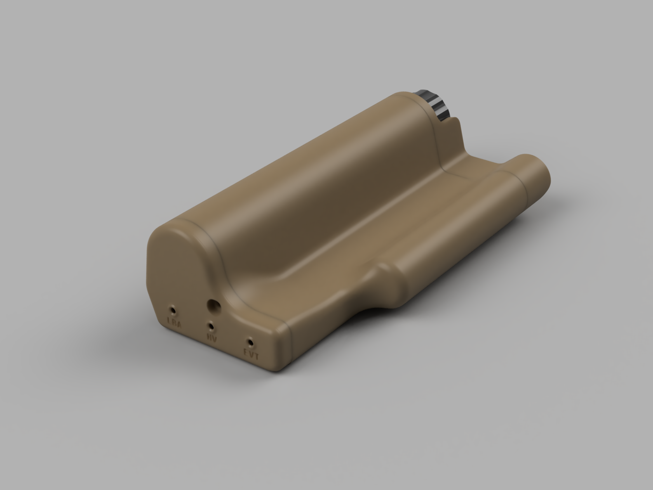
After a lot of thinking, moving the battery positive terminal to a daughterboard along with the indicator LEDs made the most sense. This uses spring loaded connectors which make contact the main PCB. The battery cover has a recess to accept the daughterboard, which will be potted in place with epoxy. This is then covered by a faceplate which also gets glued on. Since I'd like this design to be rain resistant I made two grooves for orings where the battery cap slides into the main housing. This is where most of my design uncertainty lies, because it's really pushing the limits of current 3D printing technology for these to work as expected. Hopefully I left enough room to not shred the orings after repeated use without compromising the seal. The tolerances are very tight around the oring seals, and this may end up causing waterproofing issues. I'll probably beef up these areas if I decide to make subsequent housing versions.
![]()
On the bottom side of the main housing is a circular hole for the piezo element to be glued in. The piezo element will also be attached to the PCB by jumper wires. I have had good success from JLCPCB for previous projects, so I'll be trying out their 3d print service for the first time. I'm not sure what level of accuracy I can expect, so in addition to MJF I also ordered some SLA parts in CBY resin.
I would preferred screw-oring seals instead of gluing to make disassembly possible, but I decided to abandon this idea at least for the current iteration. Designing in oring grooves and screw holes take up a lot more volume than glued connections, and I didn't want to spend a lot of hours on this quite yet. So for now I plan on gluing the pieces together with DP8910NS made by 3M, which is a 2 part acrylic adhesive specifically designed for nylon. I was able to find a 45ml tube on Amazon for $20, but elsewhere it was very pricey. Plastics are notoriously difficult to bond due to their low surface energy when compared to metal or glass. There are ways to increase the surface energy via flame or plasma treatment, which I have had mediocre success with. My extremely limited plasma treatment setup involved running a portable ozone generator inside an enclosed container for a few hours. While not technically the same as real plasma surface treatment, my theory is that the ozone should be able to micro-etch the surface of the plastic, making it more receptive to bonding. In practice, I didn't see much difference. I saw virtually no change in treated polypropylene, and only a small improvement for PET. The ozone is clearly doing something however, as both test swatches were bleached white after treatment. Hopefully none of this will be necessary if the DP8910NS performs as expected.
-
Version 2 Redesign!
07/30/2024 at 19:05 • 0 commentsIt's been over 2 years since the last project update, but recently I've revisited the design and decided to work on version 2, which should have significant improvements over the first iteration. Again, the purpose of this project is more of an exercise in old-school electrical engineering rather than trying to optimize for the usual metrics such as cost, performance, or simplicity.
I was happily surprised with the performance of version 1 given that it worked on my first attempt. However there are still a few things I wanted to improve upon:
- The power source. CR2032 cells are easy enough to come by but the battery life was sub-optimal, and I ended up using a 9V battery for higher efficiency. AA batteries are much more common and store significantly more energy then the latter two, so I needed to re-design the circuit to work from a low voltage source.
- Click volume was very quiet, I'd like the new design to make clicks that are more pronounced.
- Version 1 relies on Vbe of the bipolar transistor as the reference, and this causes wild fluctuations in output voltage based on temperature. In extremely cold environments this could cause arcing in the tube, so the new design should have tighter regulation.
Design Overview
Powering the circuit from a AA battery makes the design a little more challenging than the previous one. I decided to go with the same oscillator architecture from the previous design, since it worked well, and is able to operate down to 0.7 volts. After getting into the LTspice simulations for only a short time, I realized that a system supply would be necessary in order to achieve the efficiency range I was looking for, especially since the HV boost FET necessitates a minimum drive voltage of around 3.5V. A low voltage FET is used for the boost section of the circuit, so ensure startup from sub-volt supplies. The main oscillator is supplied from this system rail, forming a positive feedback loop. This enables the circuit to run on supplies down to 250mV once bootstrapped. While this feature wasn't part of the design requirements, it's a real plus when operating batteries below their recommended temperature range. The system voltage is regulated via a feedback loop which sends a pulse of current through the boost inductor whenever the supply voltage drops too low. There was a strong tendency for my first attempts of this circuit to soft-drive the boost FET, which resulted in increased switching losses. Eventually I converged on a configuration that's able to make sharp and consistent pulses, and this concept worked well enough to use in the HV feedback loop also.
The high voltage supply is driven by the same oscillator as the system voltage regulator, and uses the same 1:100 coupled inductor as the previous design. After re-evaluating diode options, I was able to find an ultrafast diode with a reverse recovery time under 25nS. Finding a fast rectifier is crucial for this stage, since this accounts for a large portion of the switching losses on the high voltage side. I found that additional voltage doubler stages had only a minute effect on overall efficiency, so I stuck with one stage.
For pulse detection, I'm sticking with cathode-side sensing because it avoids the high voltage capacitors and resistors necessary for anode side sensing. Noise didn't seem to be an issue with the previous version, likely because the connections were fairly short. Pulses from the Geiger tube are fed into 3 bipolar transistors, one of which triggers a one-shot timer for flashing an LED. The other two trigger the piezo driver for audible clicks. I spent several days stuck at dead ends until I arrived at the current piezo driver iteration due to the numerous design constraints I had. All my first ideas revolved around feeding the pulse from the geiger tube to a FET-inductor flyback generator that would create the click. The main problem with this approach is with the volume control. I couldn't find a feasible way of achieving significant click volume range that also worked reliably within typical component tolerances. More specifically, small changes in the FET gate switchoff slew rate created huge variations in output volume. This would only be exacerbated by temperature variations and battery voltage. Eventually, I came up with a modified joule-thief booster that ramps up the voltage across the piezo element over several switching cycles, then rapidly discharges. This way, volume level is acheived by adjusting the voltage trip level that resets the monostable latch. If the piezo driver isn't able to boost the voltage to the required level within ~600uS, there is a timeout circuit that terminates the voltage booster. The booster is suprisingly efficient when a high current bipolar transistor is used, and this topology may be viable for generating the high voltage or bootstrap supplies in future revisions.
A significant portion of the losses in the previous design came from FET switching losses. Version 2 improves this via implementation of proper push-pull gate drivers that are optimized for near zero shootthru, bringing switchoff to ~25nS. The major difficulty with push-pull drivers is in the minimization of shootthru current. This is when both the high and low side transistors are simultaneously conducting, which produces a significant increase in power consumption. I overcame this via addition of two base bias diodes, which only activate the high or low side transistors when either is within ~0.6V of the positive rail, ensuring the opposing transistor is fully off at this point.Three 220uF tantalum capacitor are needed for the circuit to bootstrap when powered from a high impedance source. Without these, the input voltage rail will sag below the circuit's minimum starting voltage. Simulations indicate that it should be able to start from a 0.8V source with an internal resistance of 1 ohm. Electrolytic capacitors would have been much cheaper, but have electrolyte drying issues in the long term. Tantalum polymer capacitors are the ideal choice because of their small size, and have superior ESR when compared to solid tantalum variants.
By far the most time consuming part of the design process was temperature compensation. Luckily LTspice is able to model the circuit's behavior at different temperatures, which made this process much easier. The P-N junctions of diodes and transistors typically have a forward voltage temp coefficient of -2mV per degree. Both the system and high voltage supplies rely on the base-emitter voltage drop of a transistor as a voltage reference. Without compensation, the regulated output will drift by +/- 18% over a -40-65 degree temperature swing, which is too loose for this application. The most common method of temperature compensation is via a matched transistor pair arranged as a current mirror. While this should result in nearly perfect compensation, I found that only one compensation stage was insufficient. Monitoring the change in the high voltage supply over temperature, I measured the temperature coefficient to be closer to 3mV per degree. I believe this is due to the fact that the regulation loop is comprised of multiple cascaded PN junctions, but I'm not entirely sure. Properly compensating each cascaded PN junction would double the number of transistors, and I didn't want to increase the design complexity this much. I decided to accomplish this by use of NTC thermistors, but there are a few caveats. NTC thermistors change resistance exponentially with temperature, versus the (almost) linear response of PN junctions. This can be linearized to a certain extent with a carefully chosen resistor network, so I wrote some quick and dirty C++ that finds the optimal resistor values for this network. You can try it for yourself here. To use it, you will have to experimentally determine the effective lower resistance necessary at 3 temperature points. I managed to find a network combination that kept the output voltage deviation within a few percent. While not absolutely necessary, I also included compensation for the piezo driver circuit, and the main oscillator. Compensating the oscillator means I can get away with less peak current headroom for the voltage boosters so they don't saturate. The piezo boost driver is less of a concern, since it begins to switches current off when the inductor starts to enter saturation.
Optimizing the current consumption of the entire design was an exhaustive task, but I was able to get it down to ~10mA at 1.2V. This should equate to >200 hours of operation from a AA alkaline cell, and is much better than I was initially going for.
If you're interested in making your own modifications, you can download the LTspice simulation, or a PDF of the schematic. I will probably have to tweak the values of a few passives after testing, but the current values should be pretty close.
Component Selection
Nearly all the specific parts in this design are rated for automotive use. It's definitely overkill for a portable device, but I wanted to design something that would still work in 20 years. Automotive components also have longer lifecycles, and most have several non-automotive alternates that are drop-in replacements.
I'm going with some 1414 size LEDs from Osram which will be massively underdriven for efficiency reasons. I like the VJLPL1 series because of the unique color options available and size.
Most passives are 0603 size because they're easier to place than 0402s. For complex designs like this, it also makes routing easier since traces can be routed underneath on the same layer. Since long term reliability is a factor I went with all sulfur-resistant resistors, except for the high voltage resistors which I was unable to find. All capacitors are C0G/NP0 dielectric which don't have DC bias or temperature coefficients, and don't suffer from aging like other dielectrics. The bulk capacitance for the system supply is a 22uF X7R capacitor, since a C0G/NP0 with this capacitance is massively impractical. Tantalum are also not the best choice due to their higher ESR. I'm not too worried about aging in this case because the exact value of 22uF isn't critical.
All bipolars are the ubuquitous 2N3904/2N3906, although others would work just fine. Substituting alternatves would likely merit a recalculation of temperature compensation networks though. The main switching transistor for the piezo boost circuit is a ZXTN4240 can handle more current.The system supply boost FET was chosen to have a particularly low Vgs so that the circuit is able to boostrap from low voltages. For the high voltage boost, I went with a 100V FET which I believe is the sweet spot for on resistance and Vds for optimal efficiency. The threshold voltage is less critical for this one, but should be as low as possible so the system voltage booster doesn't have to work too hard.
Construction
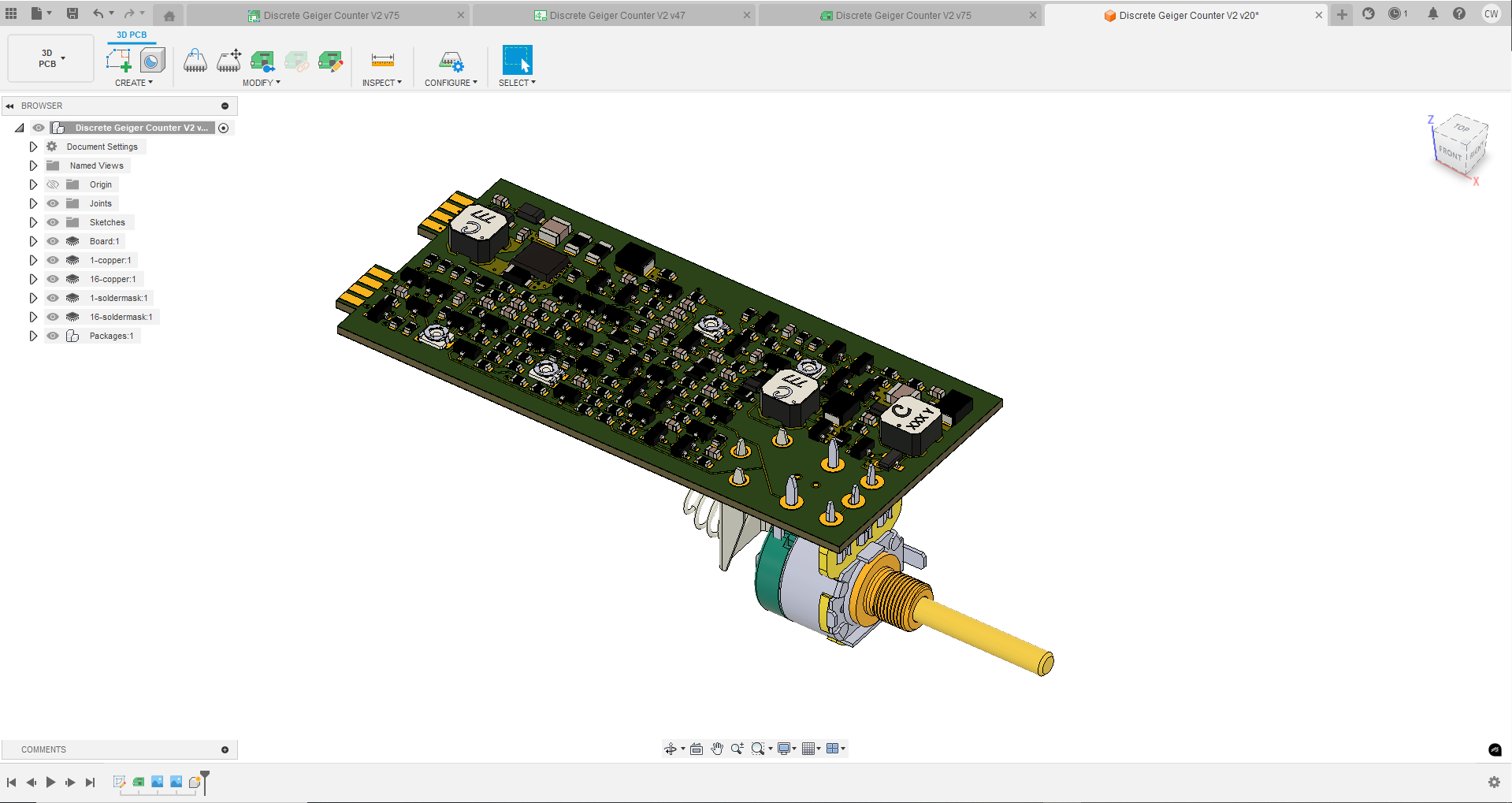
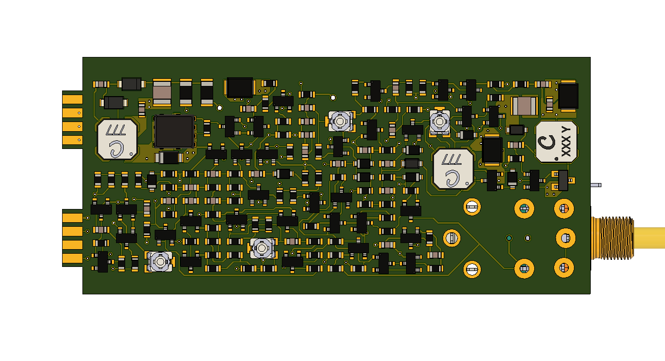
Since I still want this geiger counter to be portable, it will be housed in a custom 3D printed enclosure. This model has some pretty fine details so I will be going with the MJF process for the durability and resolution. From what I've read it's also water resistant, but I will have to do some testing once I get the models.Despite the schematic being so chaotic, PCB layout ended up not being too difficult. Most of my time was spent grouping related components together. With the exception of the gate driver FETs, I don't think component placement will matter all that much. To keep the overall dimensions small, I went with a 4 layer PCB, with the inner layers being the system supply and ground. The battery negative terminal is aligned with the volume potentiometer/power switch to make the best use of space. I left several mm of space on either side of the PCB so it can slide into slots in the internal cavity of the main housing. The geiger tube itself will be inserted into a hollowed out recess in the main housing, and the terminals will be connected via soldered jumper wires.
In the next project entry I'll go into more detail about the 3D printed parts. The models are about 75% complete, I just have to verify the fitment and make some minor adjustments.
-
Version 1 Prototype
05/13/2022 at 01:05 • 0 commentsV1 Schematic Overview
Starting on the left side of the schematic, Q7 and Q9 form a classic bistable multivibrator which oscillates at roughly 22kHz. This keeps audible noise to a minimum while prioritizing electrical efficiency. The benefit to this type of oscillator is the relatively fast turn off time of the transistors. I found a good balance of resistor and capacitor combinations that have a fall time under 75nsec, which will maximize the amount of energy extracted from the inductor every cycle. These pulses are fed into Q2 via a high pass filter which limits the current pulses through the inductor to 3uS. This is important to keep the main inductor out of saturation, which will waste energy. Also, if the oscillator gets stuck 'ON' for some reason, there is no risk of dumping current through the main inductor. When Q2 is pulled low, Vbe of Q5 drops below 0.6V, and charge from the main MOSFET gate gets pulled to ground via D3. As soon as Q2 turns off, R9 and Q5 form a voltage follower which turns the MOSFET ON. R6 prevents unwanted oscillations in the gate voltage.
When the current is cut off from L1, the inductive EMF kickback is fed through the secondary side which adds the two voltages together. This high voltage spike goes through D1 and begins to charge the main high voltage capacitor. R5 and C5 form a snubber network that technically isn't needed, but without it, there is a lot of ringing on the FET drain which will cause a lot of unnecessary RF noise. The efficiency hit is pretty minimal, and it's the 'right' thing to do. The voltage across C1 is sensed via a resistor divider network consisting of R2, R3, R4, and R7. 100Meg resistors are needed here so the leakage is minimal. At 400V, even a 10Meg divider will be the main loss of power in this circuit. 100Meg resistors are a decent balance between leakage current and cost.
When the voltage at the base of Q3 reaches the setpoint of 0.7 volts, it begins to conduct. The setpoint voltage can be adjusted via VR1. This lets you use a 100k adjustment pot, which is easier than trying to find a 10Meg pot. A crude voltage regulator consisting of R19, D6, and C12 provides a relatively stable 3.6V for a consistent output voltage across the entire battery discharge range. The collector current in Q3 is amplified by Q4, and inverted by feeding the collector current from Q4 into Q8 and Q10. Even the tiniest base current into Q8 pulls the gate of Q6 low, cutting power to the oscillator circuit. This lets the high voltage capacitor slowly discharge through the resistor divider. As soon as the high voltage line drops slightly, Q6 will turn the oscillator back on, forming a negative feedback loop. Very high loop gain is preferable, as it improves load regulation and response to transient current draw from the geiger tube. R17 and C7 form delay circuit which forces the whole circuit to squeg. While this does cause some ripple on the output, overall efficiency is much better. Q10 conducts when the regulation loop is active, so D2 will light when the output is in regulation. When the battery voltage drops too low, the output falls too low and D2 turns off as a 'change battery' indicator.
The detection side starts with R1 and GM1. Normally, the current through the geiger tube is essentially zero. When a high energy particle enters the chamber, it triggers a chain reaction of electrons that slam into the anode. The result is a pulse of current through the tube which is picked up with the high pass circuit consisting of R26, C13, and R25. This current pulse gets amplified by Q14 and Q12. VR2 adjusts the sensitivity, which needs to be adjusted to discriminate against noise. Q13 drives a small buzzer and generates the characteristic clicking sound geiger counters are known for. D5, C11, and R12 form a simple pulse stretcher circuit which flashes D4 every time the geiger tube is struck. Since the pulses are only about 100uS long, the pulse stretcher lengthens them to 20-30mS so they are more visible to the user. The whole circuit is powered by two CR2032 coin cells which provide 6V. Ironically, the LEDs and buzzer are the main power draw, as the rest of the circuit only draws ~1mA. Including the LED current, I expect the circuit to run for at least 12 hours which is plenty for my needs. C3 improves the battery life considerably, smoothing out the current pulses through the main inductor.
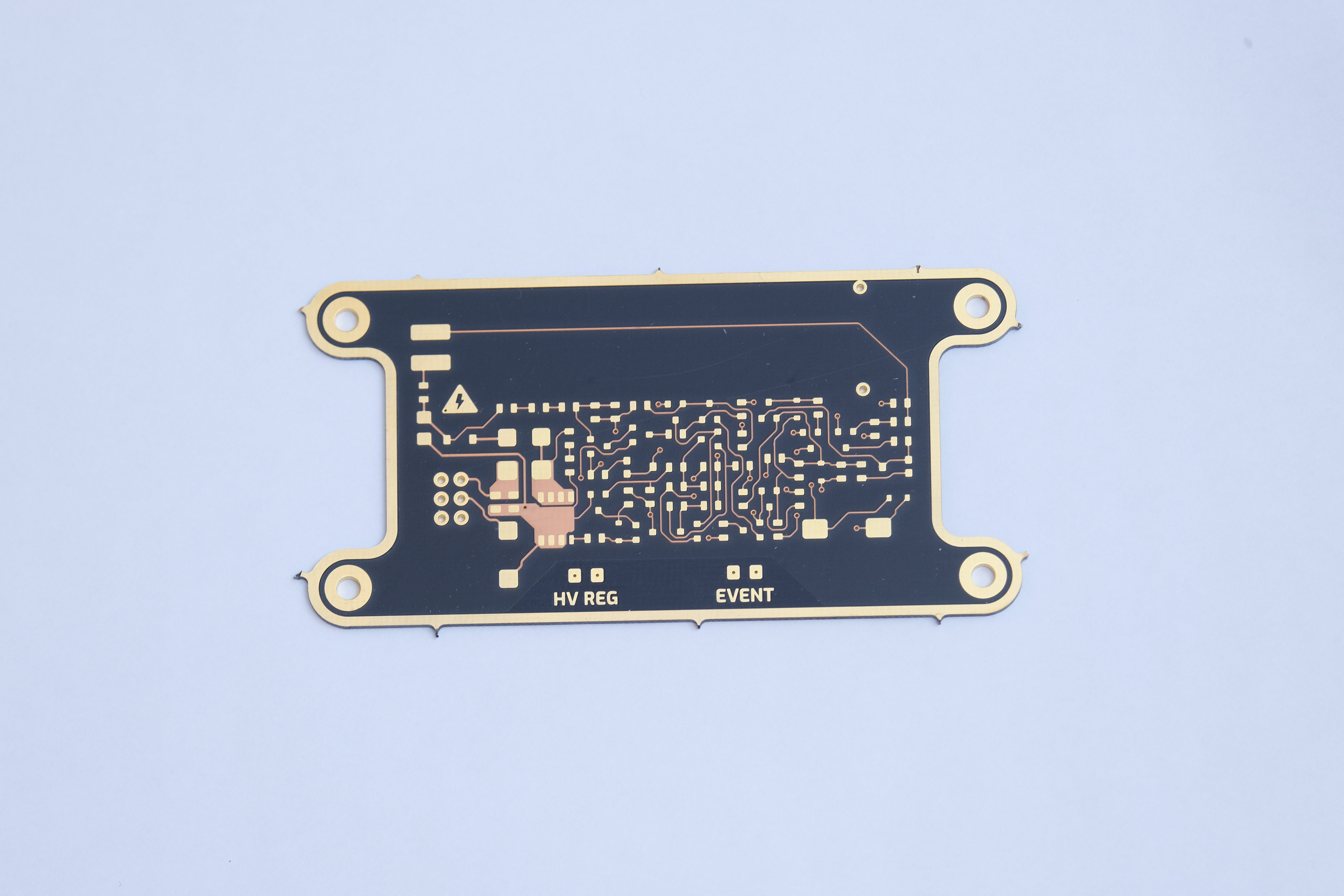
After waiting ~2weeks, I have my parts from DigiKey and 3 prototype boards from OSHPark. I'm a huge fan of their 'after dark' option, especially since it's the same price as the regular puple soldermask. The traces have really great contrast against the black substrate that give it a sophisticated-but-older look. Strangely, none of the silkscreen was printed on either side of the board, which I'm pretty sure is an error on OSHPark's part, but honestly it isn't that critical since most of the lettering was done on the copper layers.
Assembly was pretty straightforward with 0805 size components. And it passes the magic smoke test on first power up! It's always a relief when theory actually matches real life for once :) Of course, there were a few passives that needed tweaking. Nothing too major - mostly the components involving the detection side. C13 I decided to change to 10nF for better immunity to voltage drifts on the high voltage, although this shouldn't really make a difference. R24 and R27 I adjusted to give a better usable sensitivity range via VR2. With the original schematic, geiger pulses were *barely* audible through the speaker, so I reduced R23 to 4.7k and replaced the flyback diode with a 10nF cap. It's still pretty quiet, so for future versions I may experiment with lower impedance speakers or switch to a piezoelectric one. The pulse stretcher circuit for the LED was way too short initially, and I eventually figured out that the C11 wasn't able to discharge completely during pulses. Since there wasn't an easy way to increase the discharge current dramatically, I opted for a 10nF cap and 100Meg charge resistor. This gives flashes that are ~300mS long for decent visibility. Also, for reason the snubber circuit across the main FET wasn't tuned right, so I reduced R5 to 100ohm. It isn't perfect, but it's good enough that I'm not going to bother fiddling any more.
Setting the output voltage is tricky because of the very high output impedance. Even a 10Meg multimeter input impedance will drag the voltage down out of regulation. After experimenting with different setpoints, I set VR1 to ~30% of the max output voltage. I'm guessing the output voltage is 360 volts or so, but I can't say for sure until I buy or make a high impedance probe.
At 6V, the entire circuit draws about 5mA, although the majority of that current is flowing through the indicator LEDs. With a setpoint of 360-ish volts, it stays in regulation down to a battery voltage of 3.75V. After dropping below this point, the step up converter is on constantly and the input current rises exponentially to a max of 100mA. Of course, the CR2032 cells wouldn't be able to support this much current, especially when discharged to 1.9V/cell. It's difficult to find data on CR2032 capacity vs discharge rate, so I'm going to have to determine that experimentally. I estimate ~20hrs of continuous operation until the output falls out of regulation.
Background CPM is 15-17 in Oregon where I live, which seems to be typical for the SI-29BG tube. Bringing a few Uranium UV fluorescent beads close to the tube results in readings in the range of 50-70 CPM. I don't have any other check sources at the moment, but soon I will be exploring some abandoned Uranium mines where I will be able to do further testing.
Discrete Geiger Counter V2
Portable, low-power geiger counter made exclusively from discrete components
 Caleb W.


