 Open Green Energy
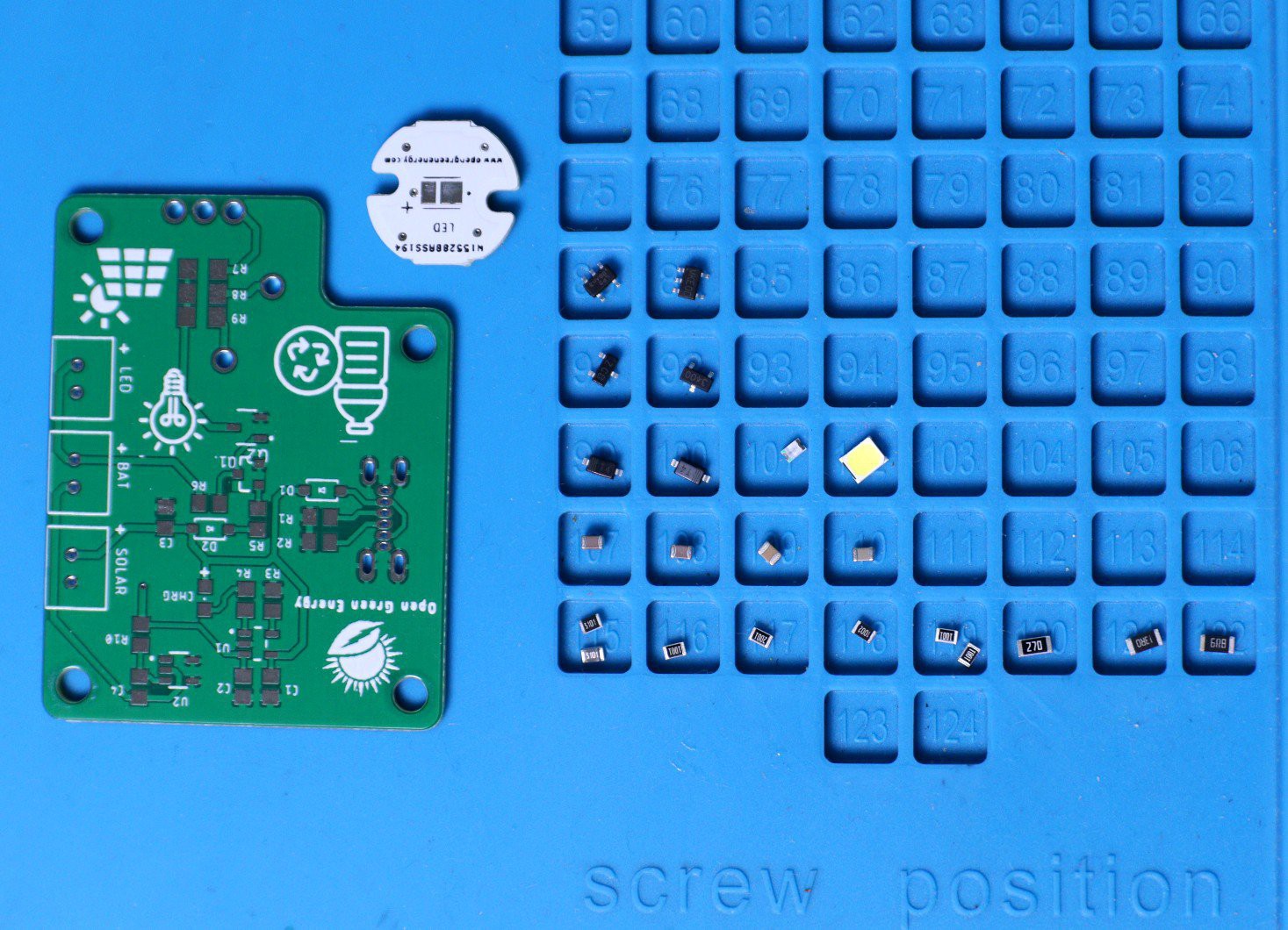
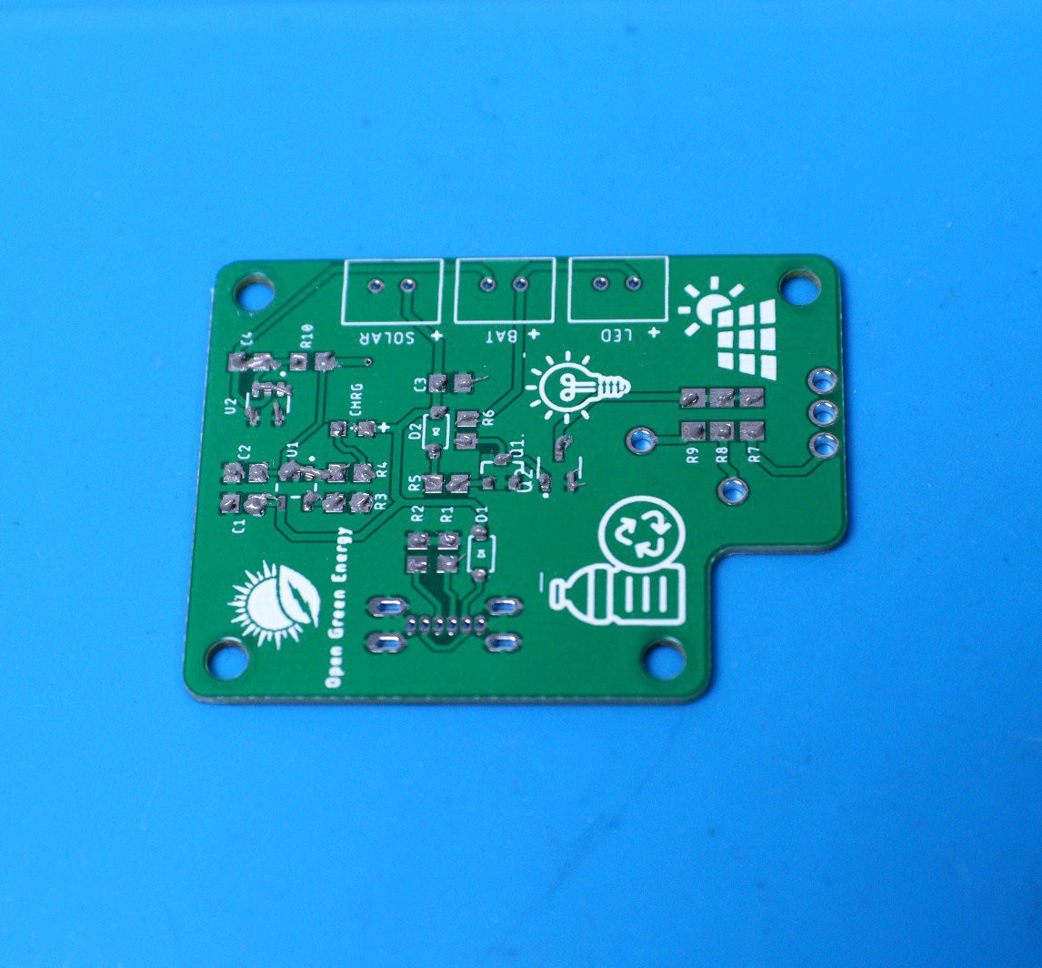
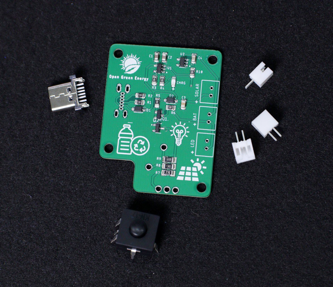
Arranged the SMD components as per the schematic diagram, so that it will be easier for placing the components on the PCB.
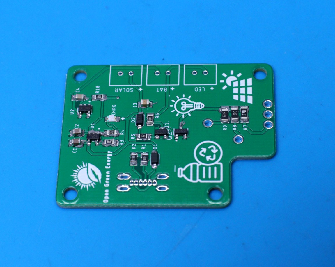
First I have applied the solder paste by using a solder paste syringe.
Placed the components by using tweezers
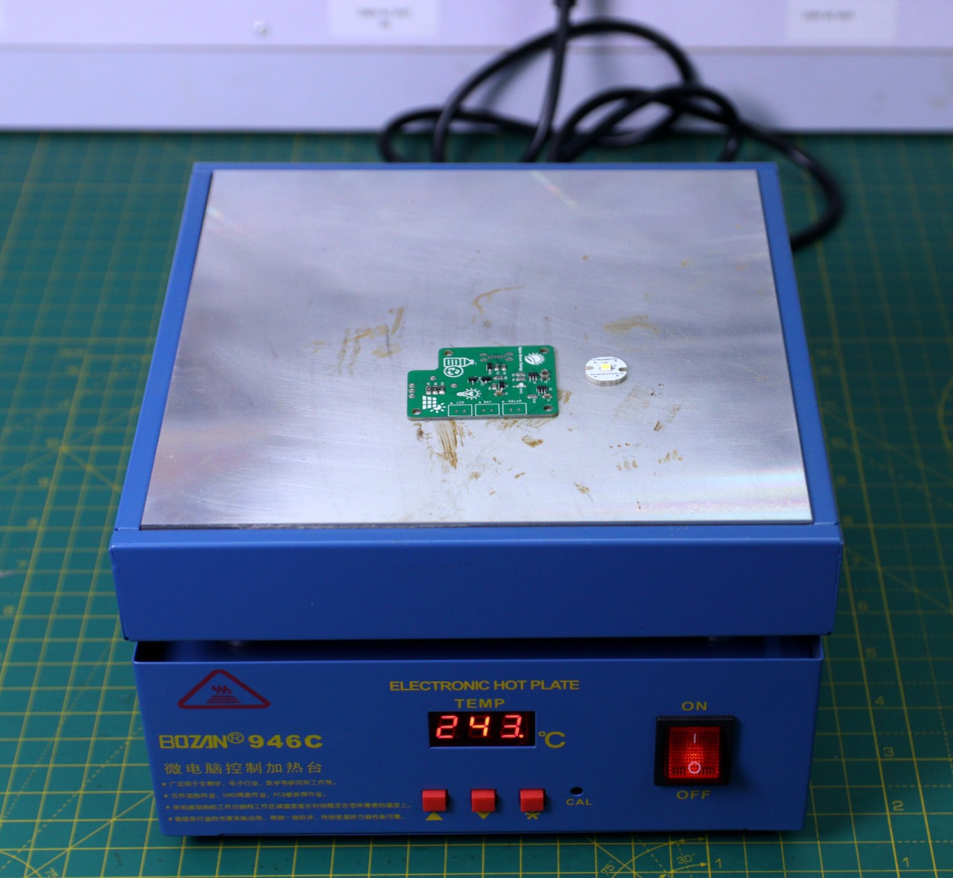
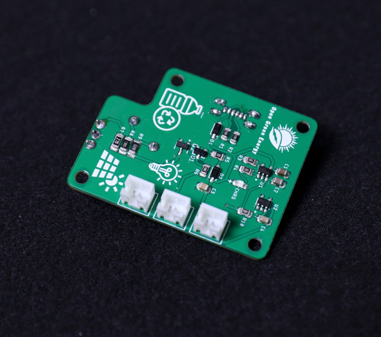
Cooked the PCB using my Hot Plate.
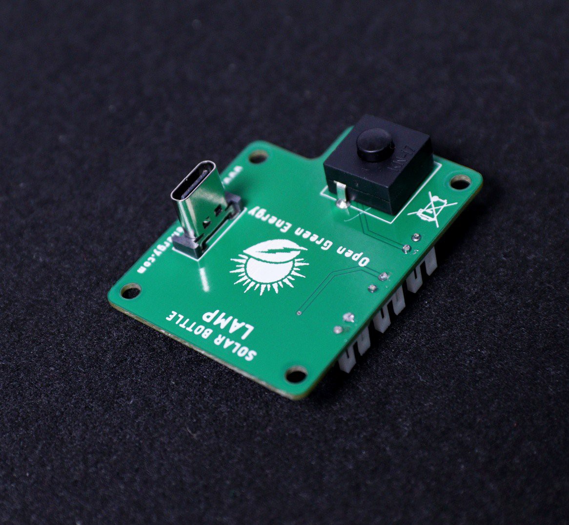
Soldered the Through Hole Components : 3 x JST connectors, Push Button Switch, and USB-C Socket
Discussions
Become a Hackaday.io Member
Create an account to leave a comment. Already have an account? Log In.