Artem Kashkanov
-
WW16 Update
04/25/2017 at 07:43 • 0 commentsDeveloped 2AND/2XOR module for carry-chain version of Adder. Just need to etch pcb's for it.
Failed first attempt of protection solder mask applying. I expected this.
I did this procedure long time ago last time.
Unfortunately my oven handles temperature with very big difference between the top and the bottom of oven. As a result - when two thirds of plate were successfully opened from mask top one third wasn't. Need to add little metal fan into oven for active convection.
Move out mask from all plates which I tried to do.
![]()
If second attempt would be failed too I will just milled boards and solder them without the mask.
-
WW14 Update
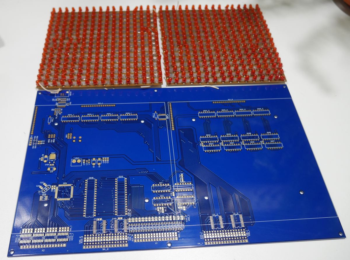
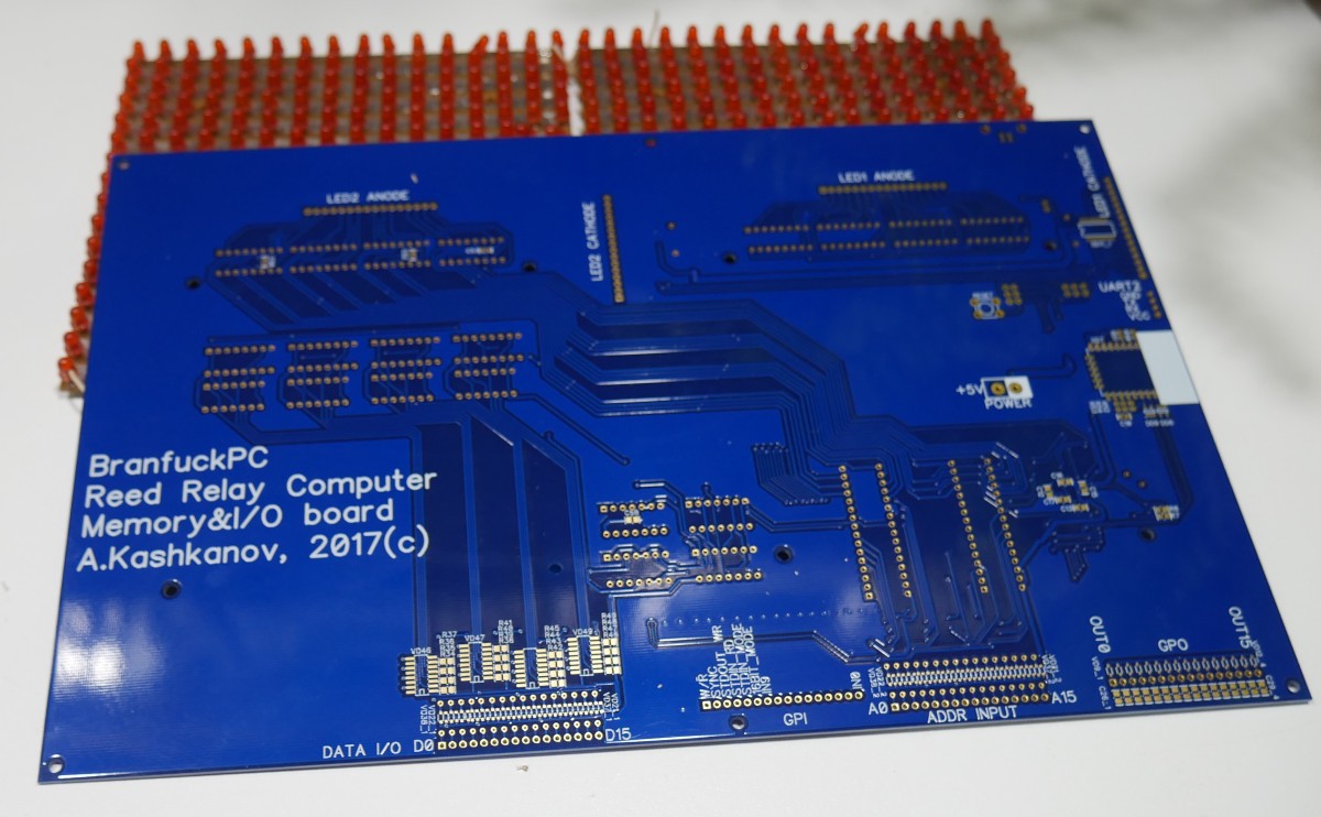
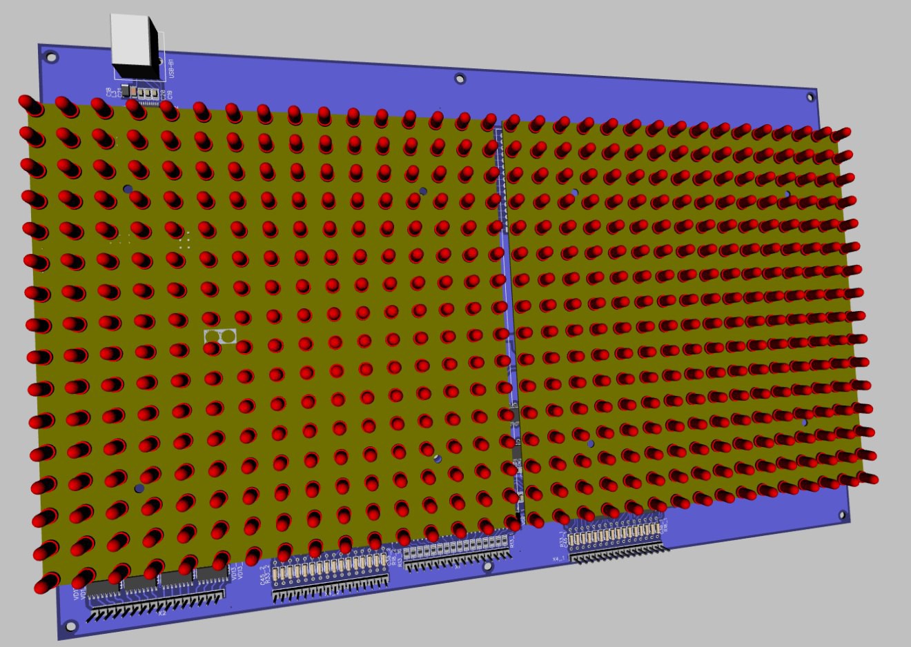
04/05/2017 at 18:26 • 5 commentsReceived memory board.. Oh man.. It look so cool. Need to start parts soldering. There are 16x16 led panels for this board. dimensions 300x200 mm.
![]()
![]()
Published an article about this board on Russian geek site geektimes.ru on the first of April. That was very good idea - My article was very popular this day.
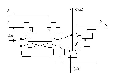
And as a result - someone in comments gave me advice how to optimize adder schematic and reduce relays for it from 256 to just 112! It's the whole block! Carry chain - is very good idea for this project.
Here is schematic:
![]()
There is an error near K4 - contacts are reversely connected. So instead of 32 modules with 3 different types (ADD+C, 2AND/2OR, 5AND) I just need 32 modules with one type! 2AND/2XOR
Will create schematic and routing for this module in nearest future.
-
WW12 Update
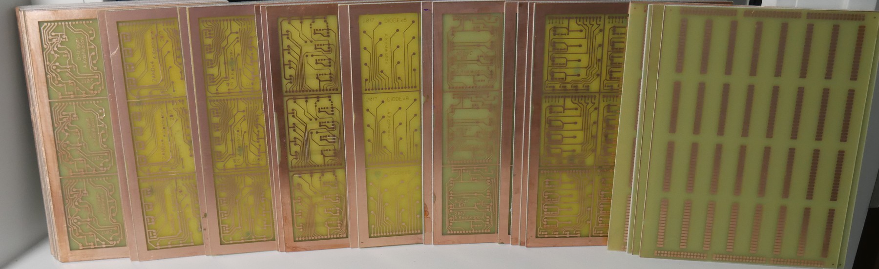
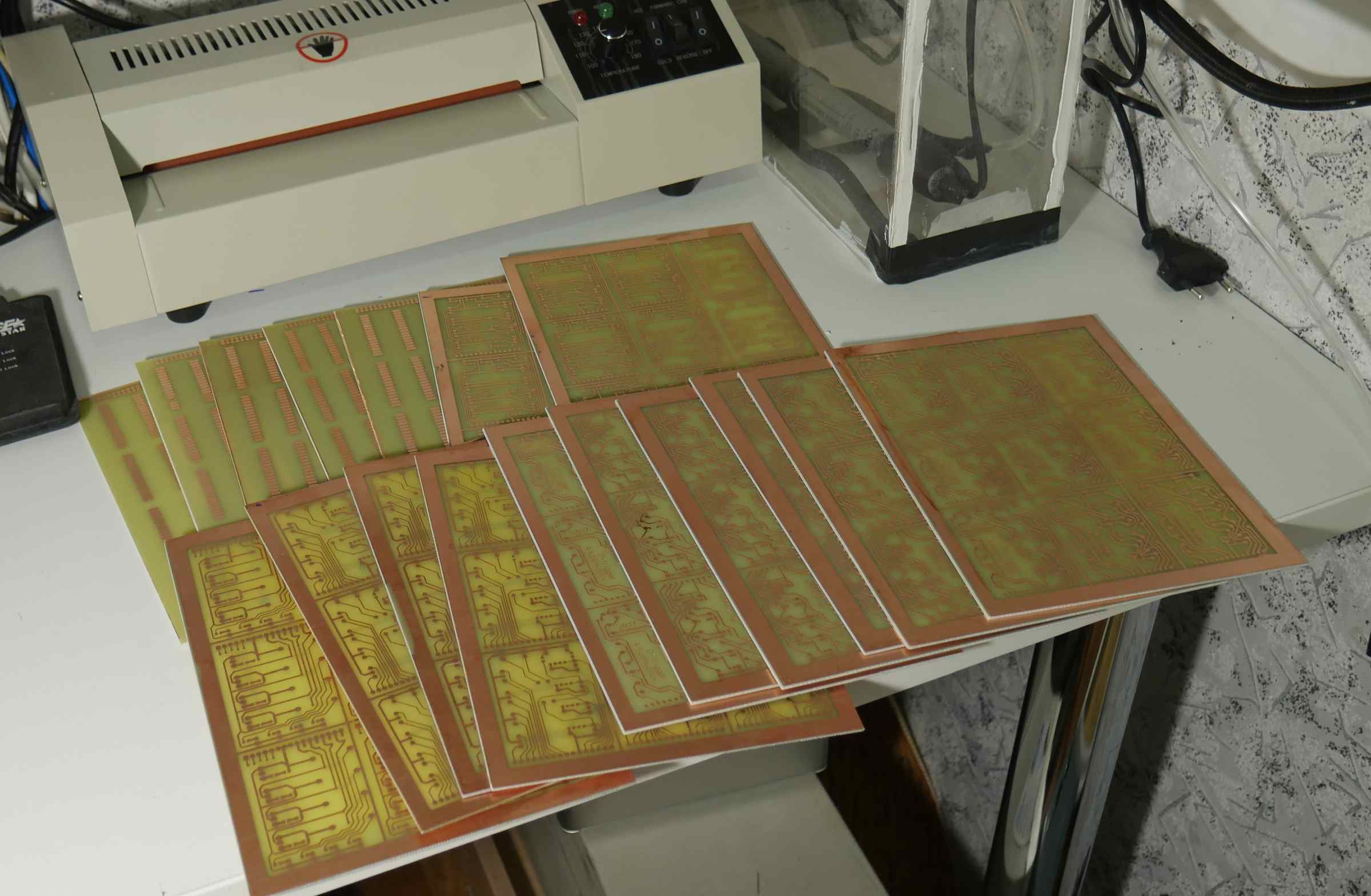
03/23/2017 at 20:38 • 0 commentsDone with etching 30 pcb plates! 8 different types. Now working on photomask.
![]()
I'm done with Memory Board and send it to manufacture. It comes back to me at the beginning of April and I will start assemble it
Here is 3D view with all parts (yes, it's 16x16 led panels on the top):
![]()
![]()
-
WW09 Update
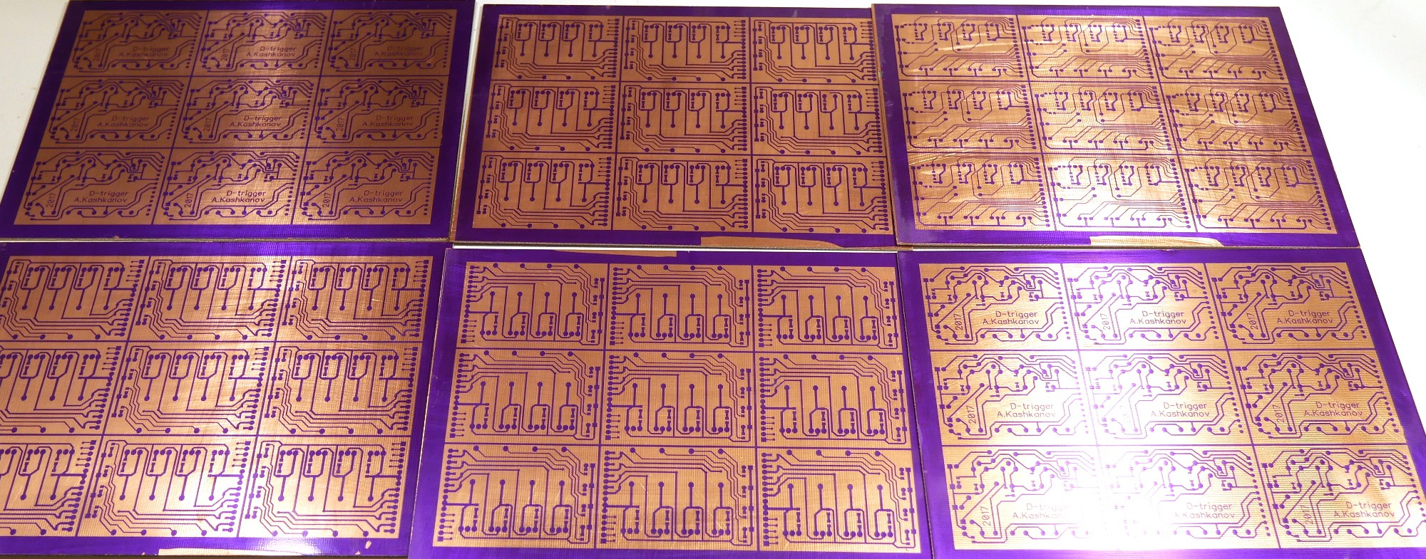
03/05/2017 at 21:07 • 0 comments- Put image to another 6 plates - 3pcs of 5AND, 1pcs of 2AND/2OR, and 2pcs of D-trigger. Need to etch them but first want to image other boards for batch eching :)
![]()
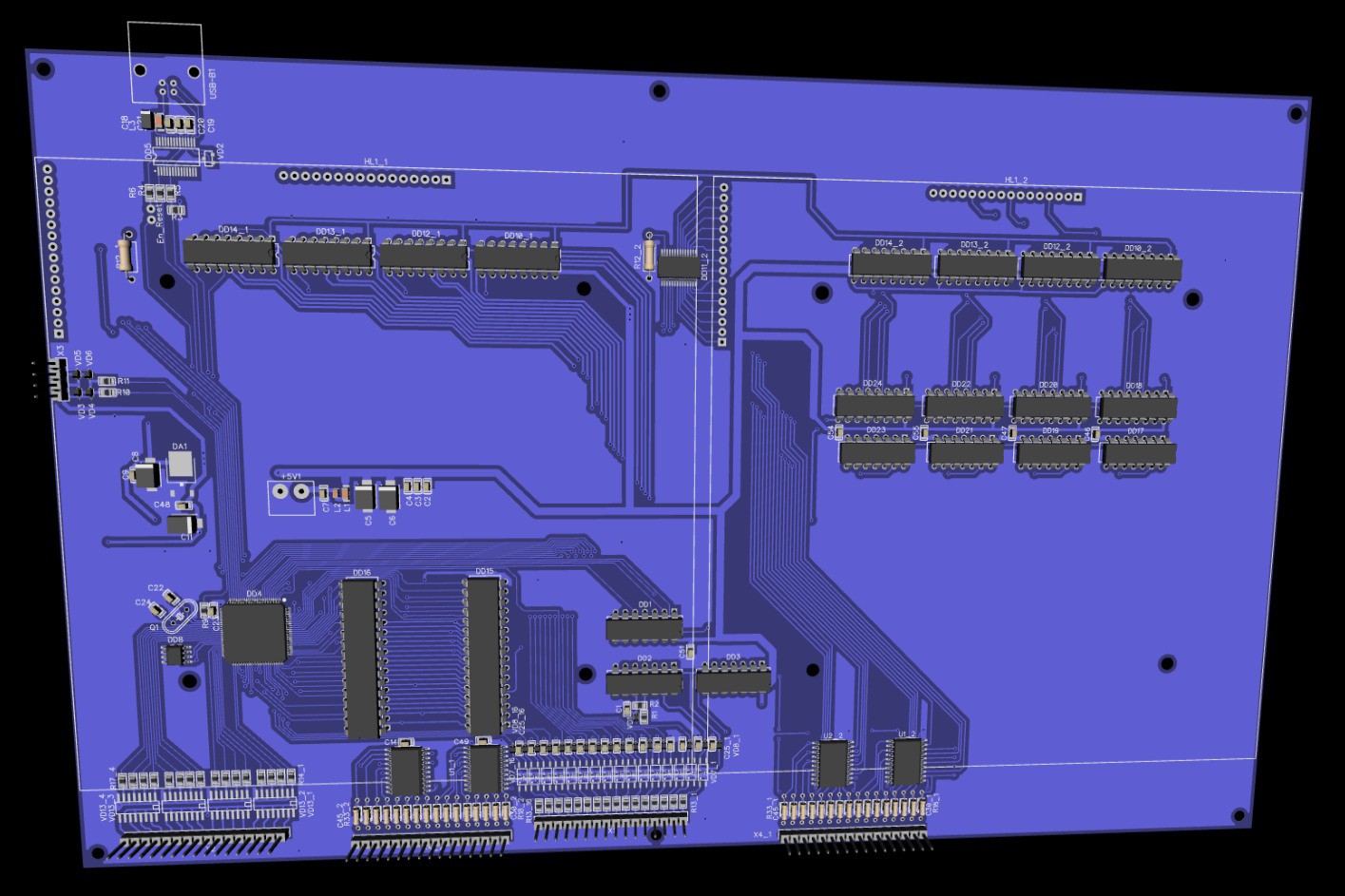
- Finished with Memory Board routing. 3D Looks very good. Yeas, Most IC's are in DIP - this is because I have a Lot of Soviet IC and use them. Need to check all connections and will send routing to pcb maker - I can't do so big pcbs (300x200 mm ) at home.
![]()
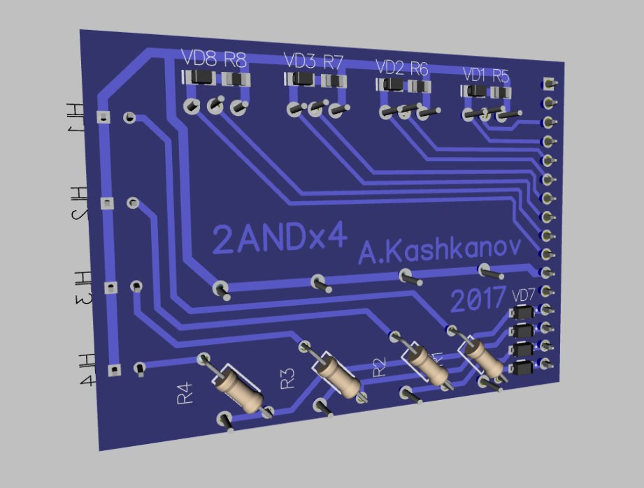
- Routed 2ANDx4 pcb - I got single-side pcb again. Will use this type of module as a key module (four modules per bus) and in sequenser module where after 10-stage sequenser and diode matrix I will need to send signals to blocks. 3D looks good. Will do this modules at home.
![]()
- Prepare plywood table for photomask - it's ready for use and I want to start when finished with all known boards.
- Put image to another 6 plates - 3pcs of 5AND, 1pcs of 2AND/2OR, and 2pcs of D-trigger. Need to etch them but first want to image other boards for batch eching :)
-
WW08 Update
02/26/2017 at 19:44 • 0 commentsI routed almost all modules:
ADD+Carry module, D-trigger module, 5AND, 2AND/2OR module, base board and working on memory module
Currently I'm working on making pcb's - I'm doing all pcb by myself using photoresist technology.
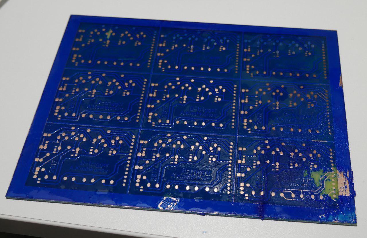
I already etched 17 of 26 panels 20x15 cm - each panel contain 9 modules and 4 relays on each module. When I finished etching I will start with solder mask.
6 pcb's - D-trigger,
2 pcb's - ADD+C
3 pcb's 2AND/2OR
5 pcb's - base panel each for 32 modules. I need one more of this type
1 pcb's 5AND - I need 4 of them for paralle carry.
I created roadmap webpage in github repository where I update all steps
https://github.com/radiolok/RelayComputer2/blob/master/roadmap.md
![]()
BrainfuckPC Relay Computer
Von-Neumann 16-bit relay computer with Brainfuck++ instruction set