Artem Kashkanov
-
Pi =4 and another relay computing bugs
03/14/2019 at 19:36 • 0 commentsTurn on subs..
-
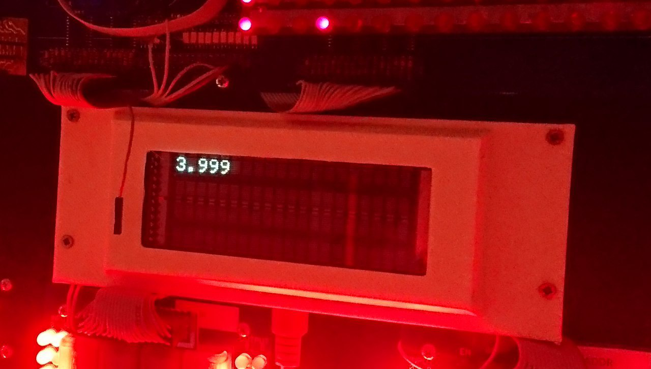
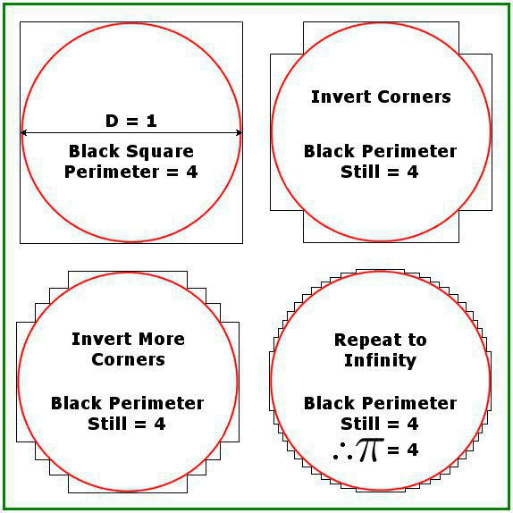
Pi = 4! My Relay computer think so..
02/22/2019 at 07:14 • 0 commentsI ran Pi program calculation on my relay computer. And after 25 minutes of calculations (~30000 retired instructions) It shows me, what he think about Pi number.
Remember this meme?
It's not a meme anymore!
-
Run Hello World on BrainfuckPC on 25Hz
02/16/2019 at 15:34 • 1 commentI connected VFD to my relay computer and run Hello world on "Brainfuck" on 25Hz
-
Perhaps, the world's fastest relay computing
01/28/2019 at 08:50 • 5 commentsFirst program works! In a cycle I'm doing ADD+ADA operations on 25Hz!
Program:
0: NOP
1: ADA+0xFF00 - set Address register to 0xFF00
2: ADD+1 //increment value in current memory cell
3: ADA+1 //shift current memory cell number
//repeate last two instruction 16 times, because writing inner loops in brainfuck is brainfuck enough :)
33: ADA-0xF //return AP to 0xFF00 memory cell
34: JNZ-0x21//if current cell is Not Zero, return IP to number 1 (which would be skipped due to pc arch).
All instructions are repeated.
-
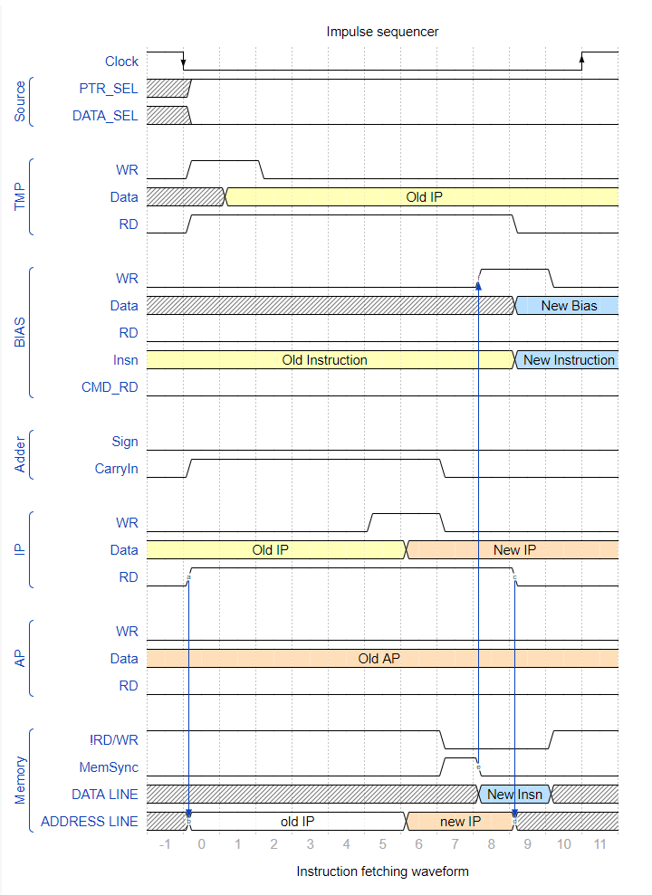
instruction fetching stage works!
01/18/2019 at 21:05 • 0 commentsInstruction fetching stage is one of two main stages - fetching and execution.
We need to write old IP register(right block, top) value to TMP register (left block, top) and using full 16-bit adder do IP+1 operation.
The result of this operation as saved back to IP register.
After we got new IP, we send reading strobe to RAM, and new instruction goes to DATA line. Now we just need to write it to CMD register (Left block, bottom) and goes to execution stage.
As RAM was inited with 0x5555 and 0xAAAA values we see how on odd IP numbers Odd bits on CMD register are flashing, and on even IP values - even bits.
Bottom line of switching boards have leds which are showing current DFATA line state and odd-even switching is observed well
With high fps camera both stages are visible very well
-
Clock system is ready
01/18/2019 at 08:14 • 0 commentsI wire-wrapped clock system! the idea is to do instruction fetching stage and execution stage in one clock cycle. So we need to run impulse sequencer two times, on every clock signal edge.
I used simple schema with XOR element and D-trigger to do this and now everything works fine.
On high-speed camera you can see, how impulse sequencer signal wave is going. And this process happened two times per one clock period.
Is Lights of impulse sequencer are flashing only ~10 ms of half-period it's funny to see how camera doesn't detect it because of stroboscopic effect.
-
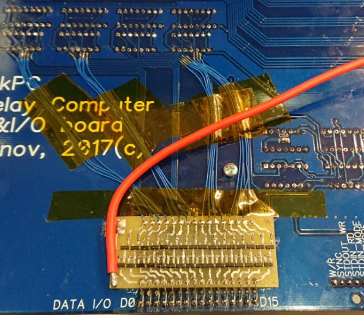
Output driver replacement for Memory board
12/06/2018 at 09:48 • 0 commentsPreviously I found, that my output drivers on TLP281-4 couldn't open just one relay... So I have to replace schematic and developed more powerful driver base on P-MOS.
-
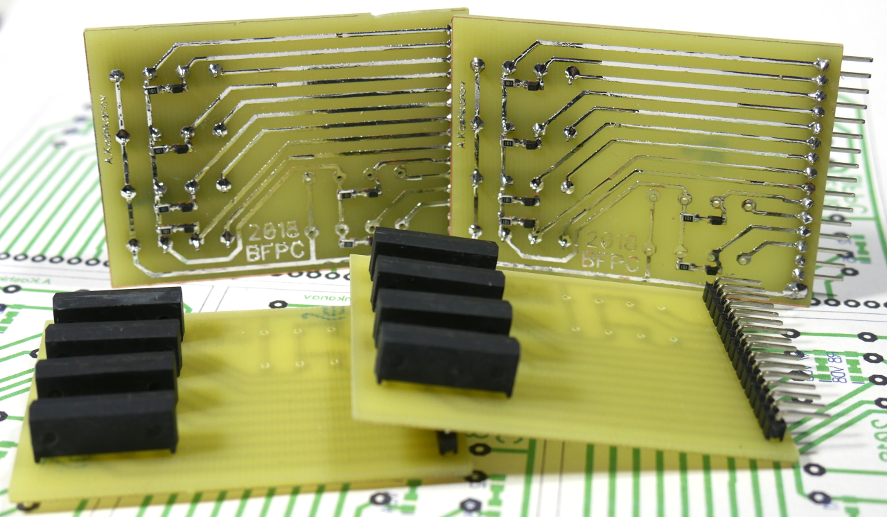
Yet another relay modules
12/02/2018 at 16:43 • 0 commentsMade driver modules for BFPC.
Control line need to be supplied with 0.5-0.7A current and my RES55 end RES64 would be broken if I will use them for this.
So I took 1A reed relays and made just a driver.
-
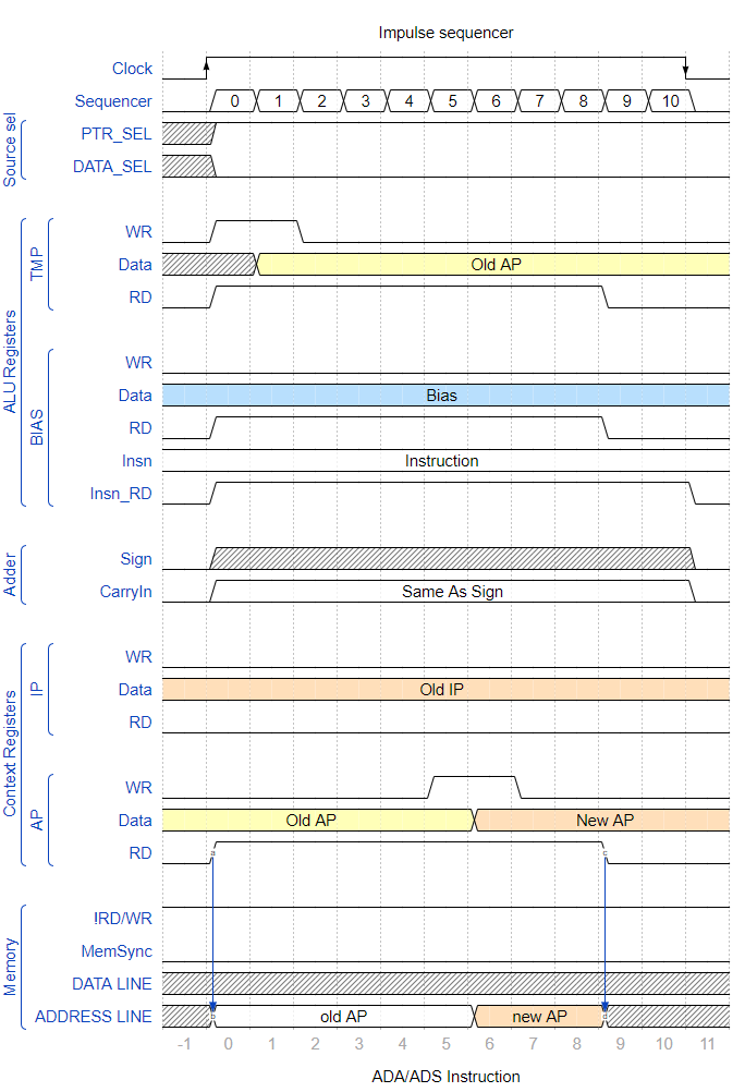
ADA/ADS Instructions timing diagram
11/21/2018 at 21:01 • 0 commentsADA/ADS instructions are used for walking through memory - we can change current AP register with some constant value.
-
Signal sequencer is not an easy task
11/20/2018 at 21:23 • 0 commentsJust created waveform for new instruction fetching - we need to do IP++ operation and with new IP address load instruction from memory.
BrainfuckPC Relay Computer
Von-Neumann 16-bit relay computer with Brainfuck++ instruction set