 danjovic
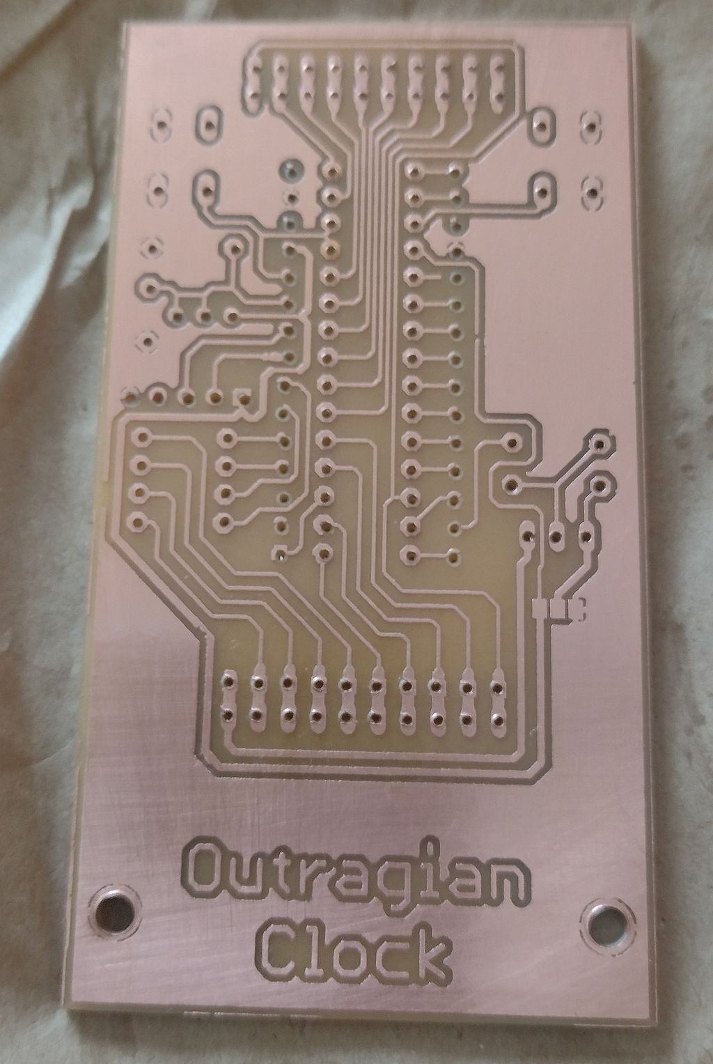
I have built a PCB at home using toner transfer method
The board was assembled and I have a first release of the code uploaded in github
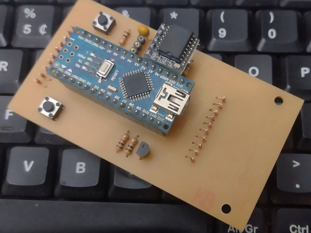
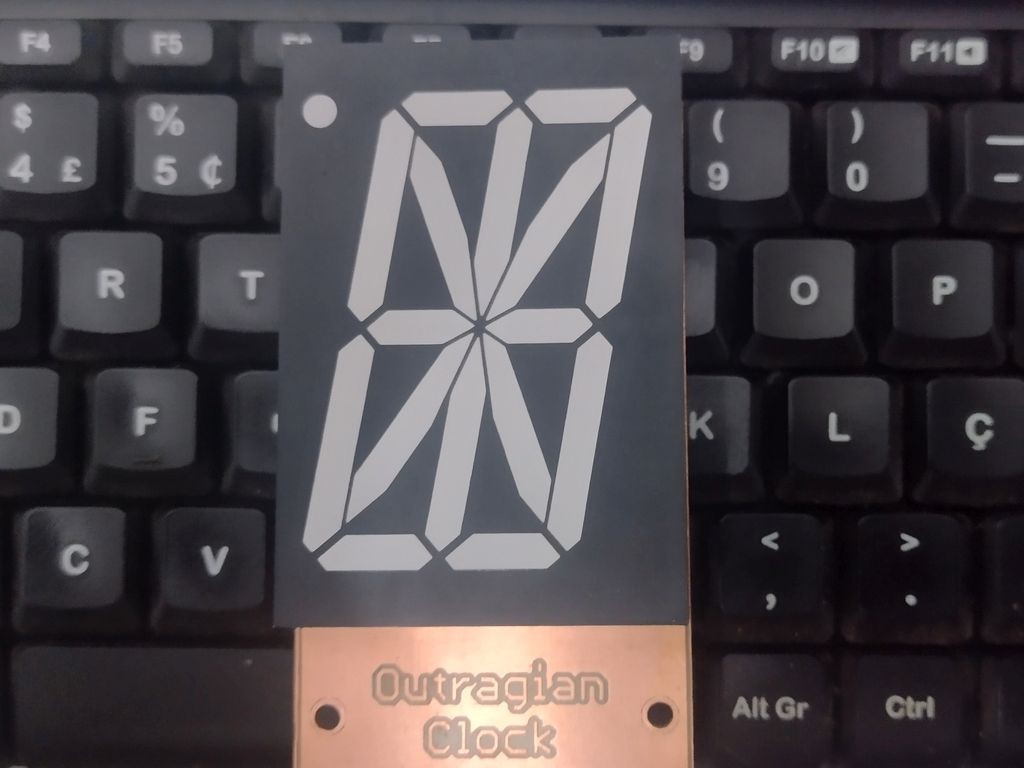
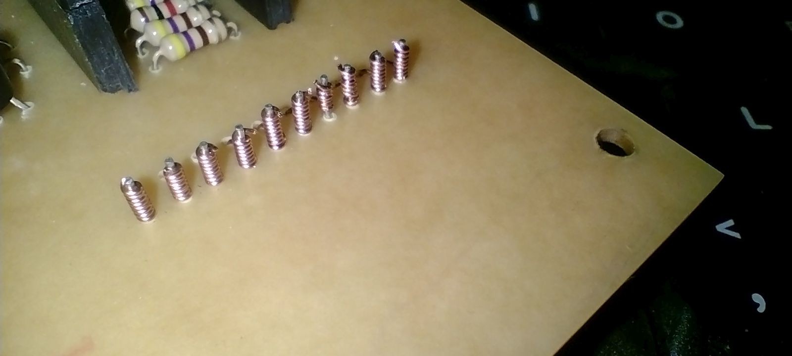
As the display is placed on the bottom the board provides holes to solder bare wires that are wrapped on the display pins.
Discussions
Become a Hackaday.io Member
Create an account to leave a comment. Already have an account? Log In.
Thanks!! It was only after etching the board that I have realized that the pads on Nano library were too small, even for my 0.8mm drill bit.
Are you sure? yes | no
That's a very nice PCB etch, well done! As you may have noticed, it's a good idea to make extra large pads just in case they erode too much, Making a "hole" smaller than actual end result helps center the drill bit more precisely.
Are you sure? yes | no