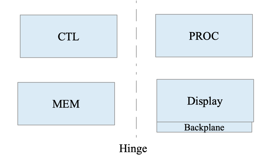
After three years I have started back up on this project. When I left off the display board and backplane were complete and the memory board was partially complete. The idea was that the board under test would be moved to the last slot of the board stack. The realization that all three boards would have to be debugged simultaneously led me to the conclusion that the board configuration would have to be modified. This has been the first issue to attack before getting back to then fun of wiring chips together. The new plan is to have all four boards exist in one plane that will eventually be placed into a frame, probably hinged down the middle. The boards will still need to be connected with various ribbon cables. The data cables defined before will remain the same, only their location on the boards will change. The display cables will change quite a bit since there will no longer be a backplane. A portion of the existing backplane was cut off. This will become a breakout board that plugs onto the bottom of the existing display board. Each group of pins relates to displaying things like registers and control pulses. These pins have been grouped into either 8, 16 or 20 bits. Each of these connectors route to only one other board. The other three boards will have these display connectors on the bottom edge instead of the huge backplane connector as before. This simplifies things significantly. The display board will have the LEDs face out and the other three boards will have the wire wrap side face out.
This is the configuration that makes the most sense.


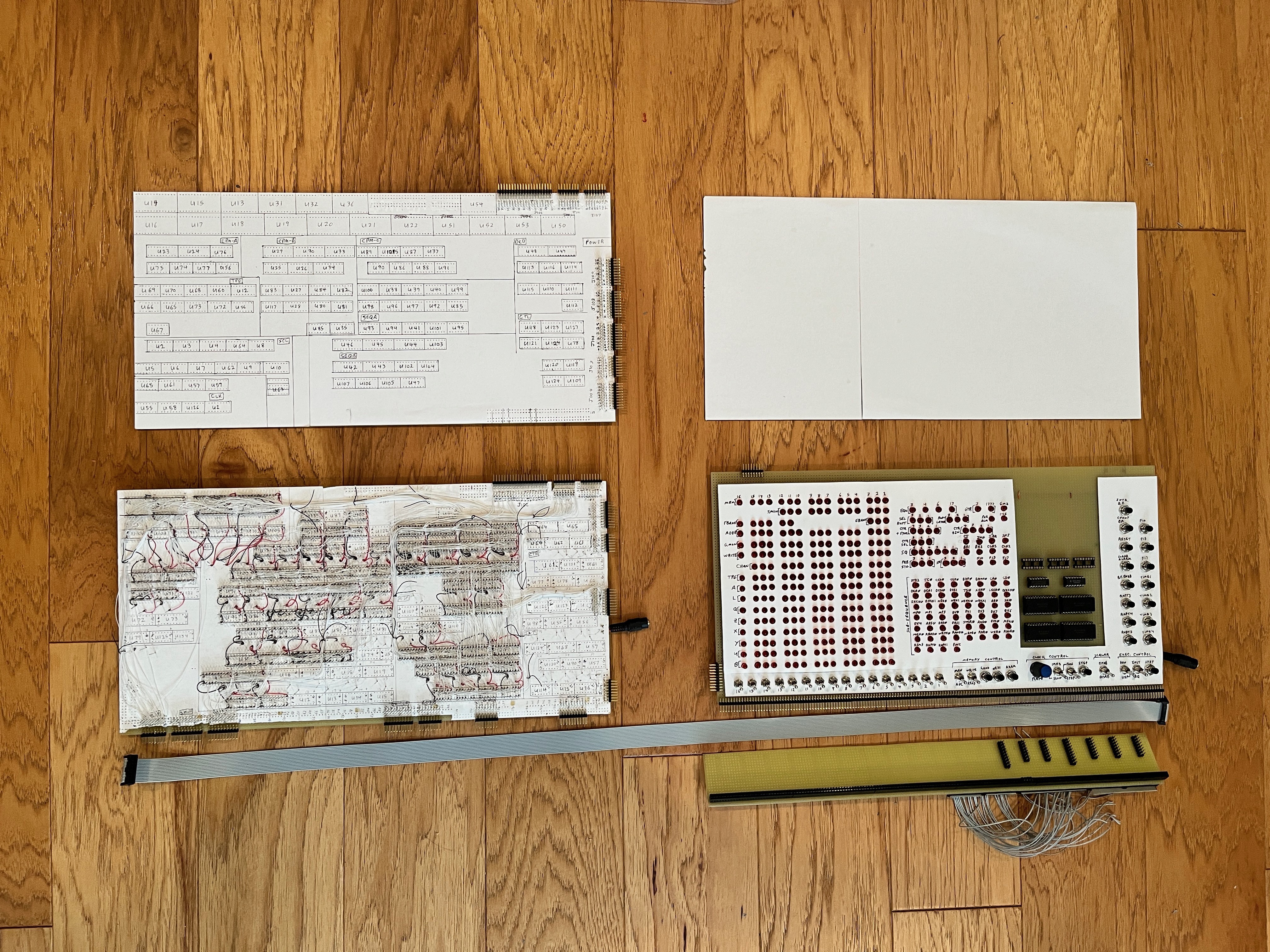
The memory board has been rewired for this new configuration. The control board only had connectors and those have been relocated. The only mod that the display board needs is the power supply connector moved to the other side of the board. You can see that I am working on the breakout board that will connect to the underside of the display board.
Once the breakout board is complete I will connect the memory board to the display board and start the process of re-verifying the wiring to date on the memory board. I stopped wiring the memory board when the realization hit me that without the display board, debugging was getting too hard.
Discussions
Become a Hackaday.io Member
Create an account to leave a comment. Already have an account? Log In.