 Guido
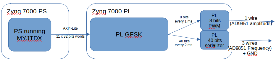
GuidoA FIFO component receives via AXI4-Lite the 79 symbols (each symbol is 3 bits each) composing the FT8 message. In this way the Linux software (MYJTDX) and the Cortex A9 CPU have plenty of time to send these 21 x 32 bits every 15 seconds. Besides, the carrier frequency (e.g. 7075500 Hz) must be sent to the AD9851.
Therefore the message from PS to PL could be composed by the following 11 x 32 bits words.
MSB LSB
- R0 : Phase shift for the carrier frequency (when symbol value=0): 32 bits
- R1 : Symbol 8 (4 bits) Symbol 7 (4 bits) ... Symbol 1 (4 bits)
- ...
- R10 : Symbol 73 (4 bits) ..... Symbol 79 (4 bits) Symbol 73(4 bits)
- R11 : 0 ... ... 0 PWM max value (8 bits) TODO
NOTE Please note that an FT8 symbol (0...7) could be encoded with 3 bits but for AXI4-Lite convenience (8 bits alignment) I decided to encode a symbol in 4 bits leaving the MSB at 0.
TODO: PWM Maximum Value
Lately I added the R11 register where I program the maximum DC value that the PWM can reach.
E.g. If I set PWM max value to 153, PWM can go from 0 Volts (duty cycle 0%) to 3.3 x 153 / 255 = 1,98 Volts.
This parameter, programmable by myjtdx (PS side) allows to be sure that when the PWM DC level is:
- at its maximum value, the AD9851 outputs nothing
- near the maximum value, the AD9851 outputs a minimal signal.
As I already built the AD9851 PWM and AD9851 serializer, it's now time to design the GFSK IP.
Discussions
Become a Hackaday.io Member
Create an account to leave a comment. Already have an account? Log In.