UPDATE: Thanks to an insightful comment by Doug Merrett You CAN relocate the board ID on boards produced by JCLPCB using the following directions.

Its finally here!
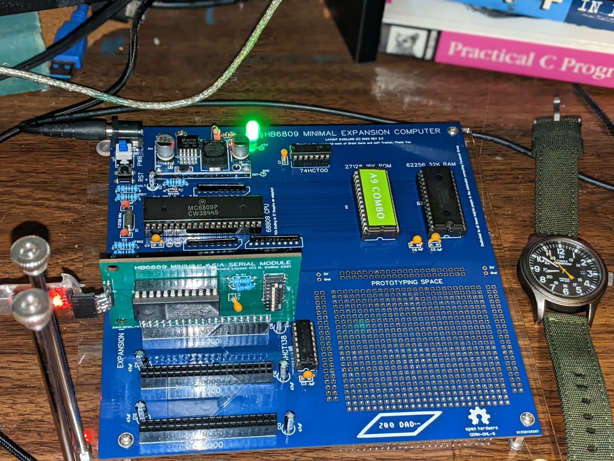
As of today, I am considering the main build complete. There's still quite a bit of work to do in making some fun optional modules for the computer, but I am comfortable releasing the build files to the general public for anybody to try out. It has been a ride for certain! I wanted this to be a fast, no-nonsense project. here we are roughly 2 months out start to finish. I can't even believe it myself, back in July I didn't think I'd get this far by now but it's basically a complete project. If anything, this really has been the pallet cleanse I needed after coming off such a complex build that, in the end there wasn't much in the way of results. What a relief to finally be here.
Final Road blocks and hurdles cleared:
if you've been following the build on Facebook, then you'll know I made a slight mistake during final assembly, resulting in some parts being damaged. If you compare the two boards assembled in pictures then you will see that I have a bog standard Motorola (45 week of 1984) 6809, instead of the proper speed grade 68B09, which the board calls for. I've since ordered the right CPU's from a recycler in Texas and they should arrive soon. The issue came in when I was getting ready to test the lines with the scope, I forgot that I had the board powered on, and when I went to solder the lug to the ground pin on the power supply module, something happened (I still don't know what, but I'm in process of doing some testing to determine exactly what). As soon as the soldering iron tip hit the pin on the module the voltage on the 5V line spiked the LED got very bright and I managed to fry out my circa early 2000's 6809 chip, a vintage eprom, and a hand full of TI 74HCT chips. I suspect that it may have to do with my soldering Iron not being isolated properly but also could be simply that the module is not designed to be soldered to while its in operation, the end result was I had to burn a new EPROM and switch out the CPU for the other one in my collection. It's running happily clocked twice it's rating; I won't run it this way for long but I wanted to make sure the final boards were working before releasing to the public.

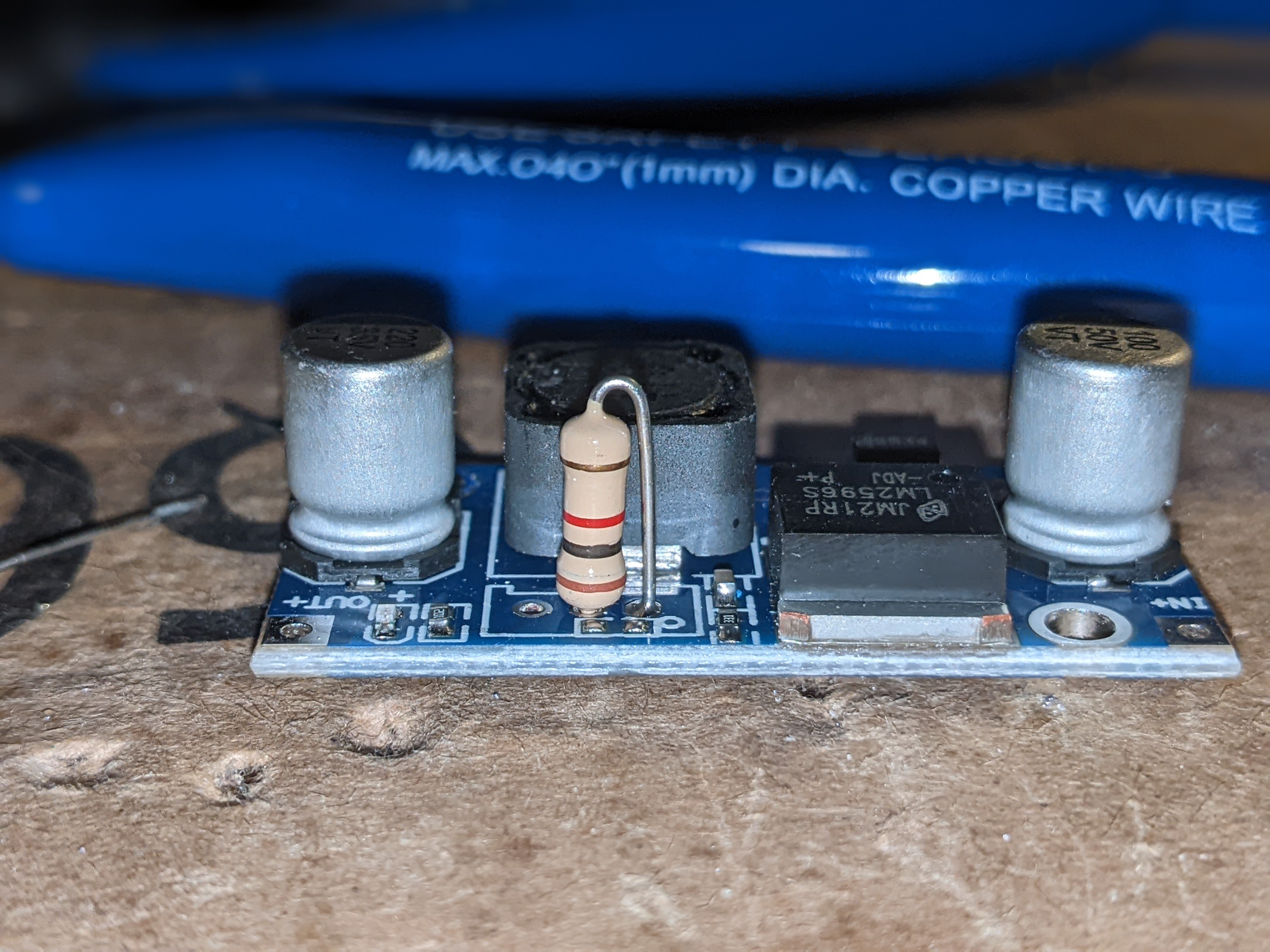
I made a small change to the DC-DC converter module, I removed the high turn potentiometer and replaced with a standard 1/2 watt, 5% 1K ohm resistor. This provides a steady 5v output, without the worry of the pot becoming scratchy, getting bumped or turned. It's absolutely optional but since it was a very easy mod to make I did it because it's some piece of mind really. If you look closely you can see there's a SMD pad which essentially routes to the same location as the through hole pads, so that you can use a simple SMD resistor (it absolutely doesn't have to be 1/2 watt tolerant, this is just what I had on hand ).
V2.2 of the PCB - PCBWay / JCLPCB PCB Comparison:
I will start out by saying, I am looking at these boards like a hobbyist would. I'm not a quality control engineer, so I can only write what I see but the question does get asked, Is the higher price of PCBWay from start to finish for a plated through hole HASL 2 layer board worth it? I think the short answer is yes, but let me spell out a few of my observations so you can get an Idea of what I am seeing. I should also point out, PCBWay, our build sponsor has covered the cost to fabricate the final test boards, However they aren't reviewing my thoughts or requiring me to say anything in particular in my review, what follows is simply my honest opinion on what I see between the two boards.
Finish (Solder mask):
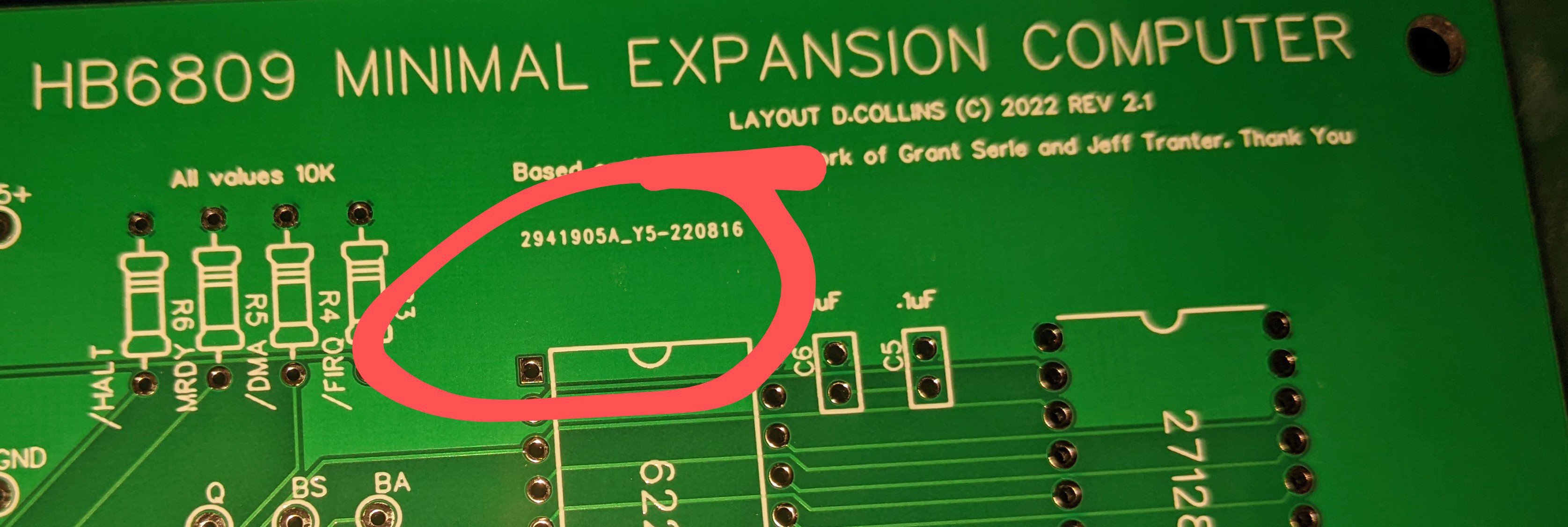
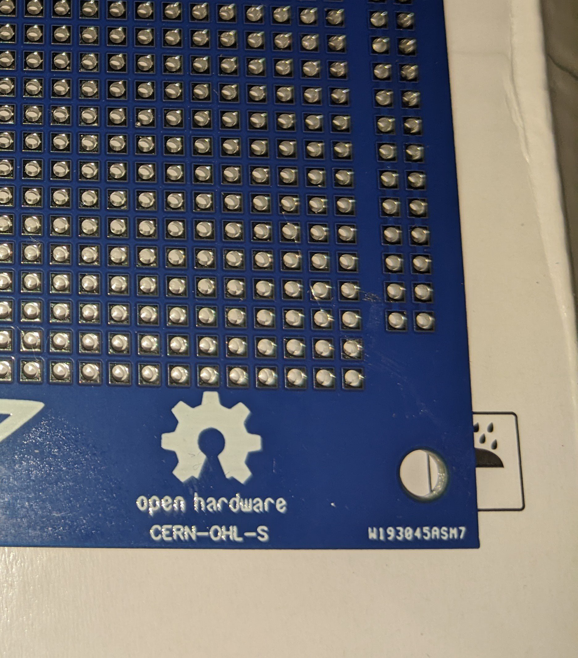
JCL's solder mask comes off exactly like what you would expect from a rapid turn prototype, it is very blotchy in places and doesn't look like a finished product should (although its important to remember its not, its a prototype). Additionally they charge extra for changing the color, and it looks like they go out of their way to put the order number in a prominent location on the PCB. Which is kind of frustrating if your particular about those things. See the update notes preceding this entry for a solution to this

The boards from PCBWay had considerably more uniform solder mask. Results are very high quality and do not look cheep. Additionally they allow you to select from a few different colors at no extra cost, and even though they are prototypes, they come off as being almost a finished product that you could put into a box as a kit and send to a customer. If they spend as much care and attention on the more higher end finishes than they do on HASL its easy to see the cost is explained by just to this level of care and detail simply spent on the one thing that is plane and visible when you pick up the board, the solder mask. As you can see they put the order number in a discrete location on the board -- as removing this order number is a value added service (just a few dollars) it almost seems like JCL went out of there way to put it in a location that would be a nuisance, as were PCBway simply put it in the lower corner, which has been my usual experience with them.

Milling and edge finishing:
The milling was spot on by both manufacturers, the plating was only applied to the through holes in locations were they were required, the vias were perfectly installed and I found no issues with either of the boards (save the one design mistake I made on the 2.1 prototype, which is hardly the fault of the manufacturer.) The edge finishing on the other hand was how the boards differ. There was a distinct softness, and minute rounding of the finished boards from JCLPCB. This led me to think that the edges were cut in such a way that they would need to be manually finished to remove sharpness left by either cutting the boards to quickly or with a manual circular saw; instead of routing them in place with a bit sharp enough to bring the edge to the specification, without making it overly sharp. The PCB's from PCBWay on the other hand were cut exactly 170 mm x 170 mm, there was a very firm right angle but the edge was not sharper than one would expect on something that only gets minimal situational handling. My only concern here is that the PCB edge tolerances could be slightly off as a result of softening the edges by a mil or two; and this could result in a PCB not fitting into a custom cut housing if tolerances are very tight the board may be loose in that situation. This is absolutely a rare situation, but if ordering PCB's from JCLPCB this has to be a consideration.
HASL finish:
Both boards had perfectly done HASIL finishing on them. Its hard to be critical on something as basic as the low cost finish done to prototype PCB's. I did try to do some minimal rework in course of soldering components and everything held up well on both boards.
Reflections:
I think the higher cost of the PCB's from PCBWay is more than justified if you have a finished product you'd like to get some boards made for, or for low volume kit fabrication its nice to know that what you are sending out the door is going to be a finished product, that looks like one, Even if the buyer didn't select the highest end finishes. JCL's PCBs while functional would not be good for this purpose, however they are more than sufficient for a run volume of one, or two boards when you are simply trying to verify if a design works, and I think that is there niche.
What is next:
The next course of action is to get a few modules built. I have all the parts on hand to make a resonablly useful sound module, but I'd like to integrate it into the same module as a VIA so that I can use the built in timers, as well as the added IO for a NES/SNES style input. Additionally, I'd like to make a priority interrupt controller, as well as a keyboard interface; for this i will likely use a 8051 micro controller, since it's practically purpose built for doing these tasks. Another thing that I am kicking around is an enhanced serial controller (like the Zilog SIO2) I would like to have hardware flow control for the serial adapter and the ACIA is really not well suited for interfacing with today's modern PC's. Lastly In the back of my head I want to make some sort of VGA interface, I'd like to make something that has input and output registers and manages the video ram internally (sort of like a modern video card), Im toying around with adding a optional header mod to the prototyping space behind the case exposed lowest expansion slot in order to provide DMA signals to just that location for enhanced graphics memory to memory copying.
Conclusion:
What an absolute journey this has been! I have to say thinks again to everybody who helped make the HB6809 a reality! The folks over at the Minimalist Computing group on Facebook, have been absolutely invaluable to everything I've done here. And of course not to mention PCBWay stepping in to bring everything across the finish line! What a wild ride this has been. I've put the links to the build files, on the GitHub up in the summery so that everybody can try out, and check out the boards. Thanks again for taking the time to check out my project!
 Dave Collins
Discussions
Become a Hackaday.io Member
Create an account to leave a comment. Already have an account? Log In.
JLCPCB for no fee will put the order number on your board in a position of your choice by just putting a placeholder on the silkscreen layer. I always move mine to under an IC or a header where it won't be seen. https://support.jlcpcb.com/article/28-how-to-remove-order-number-from-your-pcb for more info. Removing altogether is a fee, however just put JLCJLCJLCJLC where you want it. It has to be a certain size font though.
Are you sure? yes | no
I never knew this, interesting! I'll have to look into it. Thanks for letting me know I'll put your link into the review section after I check it out maybe later today :)
Are you sure? yes | no
No probs. Thanks for the overview comparison.
Are you sure? yes | no