-
1Prepare a 3D-printable file with PCB stencil
I'm using the following software: KiCad, Blender and Cura.
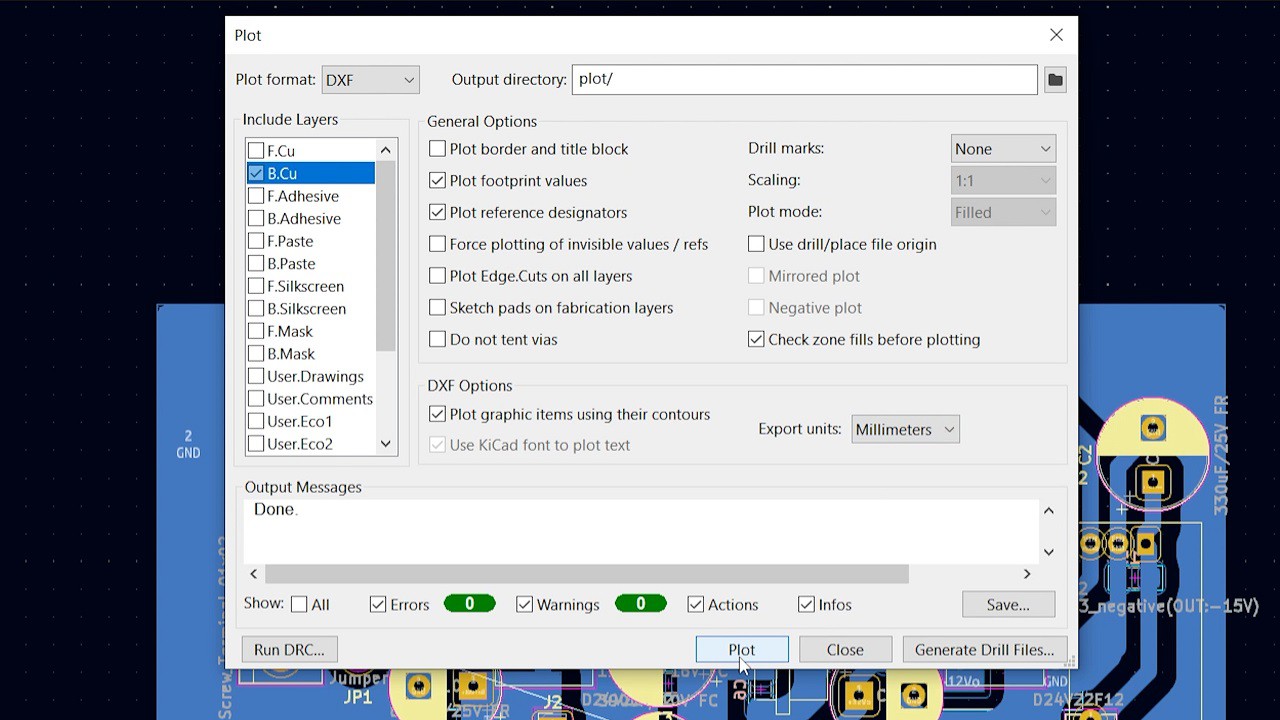
1. Open the PCB design in KiCad and plot a DXF file with a chosen copper layer.
![]()
2. Open the attached pcb_auto_template.blend file in Blender.
3. Make sure that DXF import add-on is installed in Blender (Edit - Preferences - Add-ons - find and check Import DXF)
4. Import the DXF files into Blender (File - Import - AutoCAD DXF)
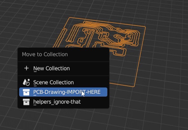
5. Select and right click the imported drawing. Move it into PCB-Drawing-IMPORT-HERE Collection:
![]()
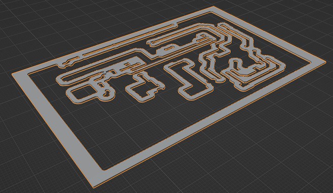
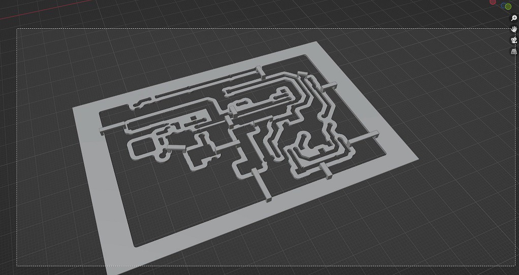
6. The stencil should be automatically generated thanks to the geometry nodes setup that was prepared in Blender template.
![]()
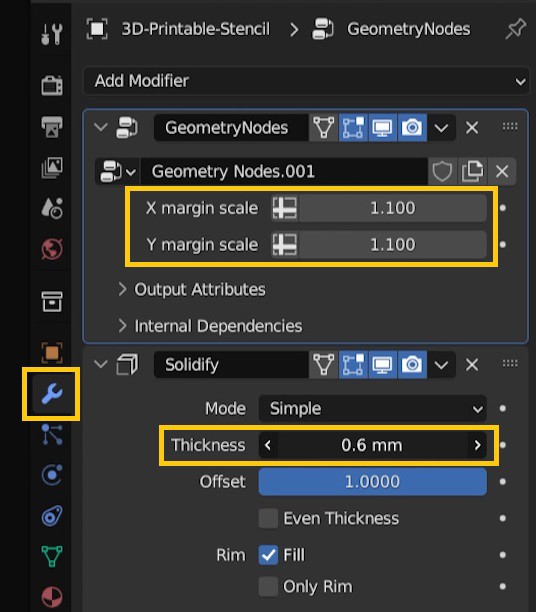
7. Stencil thickness and margin size can be adjusted if needed.
![]()
8. Now it may be necessary to put some "bridges" over the stencil, to keep it from falling apart. Some pieces were already included in the template file. They can be rotated, moved around and duplicated.
![]()
9. Now the entire stencil should be selected and exported as STL file (File - Export - STL option). Make sure to select "Selection only" option when exporting.
![]()
-
23D printing
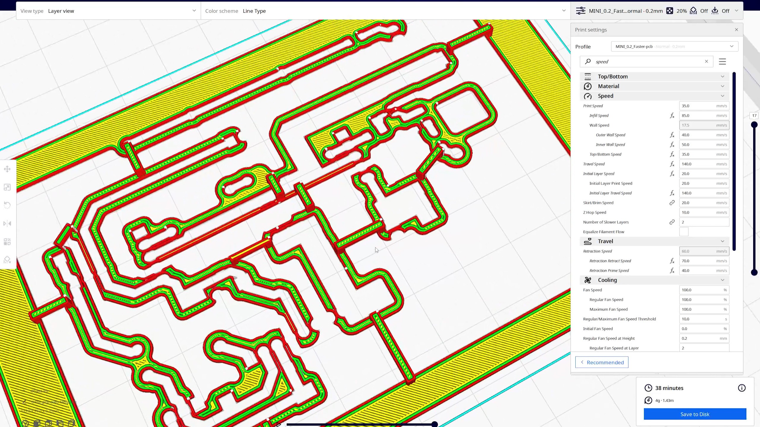
Now the STL file should be sliced in favourite slicer (i used Cura) and 3D printed. The file can be mirrored before printing if necessary.
I'm using some expansion options to make the holes and clereances a bit larger:
- Horizontal Expansion -0.04mm
- Initial layer expansion -0.04mm
- Hole Horizontal Expansion 0.05mm
I also slowed the print down by around 50% (this needs to be experimented with).
![]()
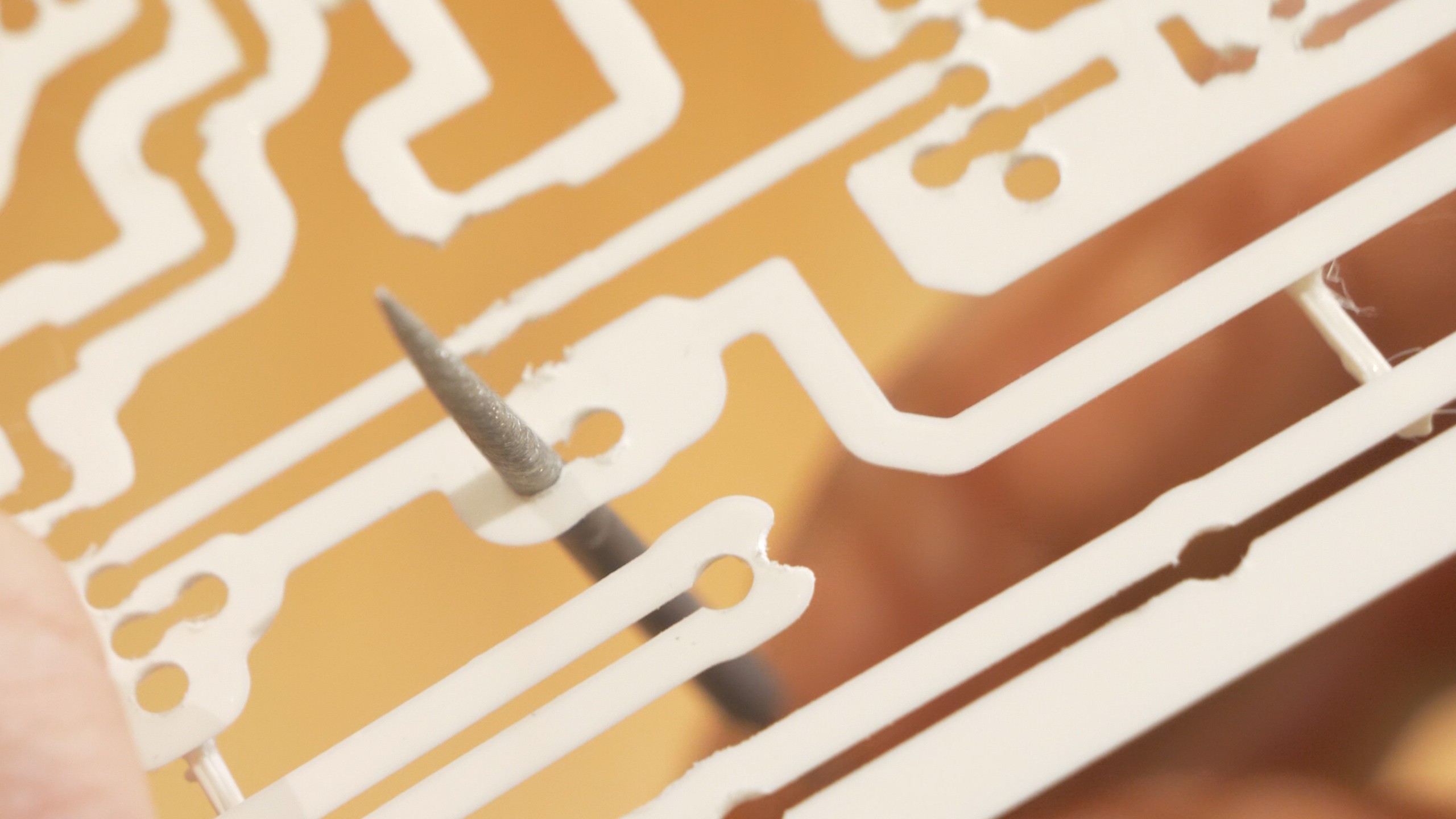
After printing it may be required to do some minor post-processing, to further increase the clereances:
![]()
-
3Preparing the PCB
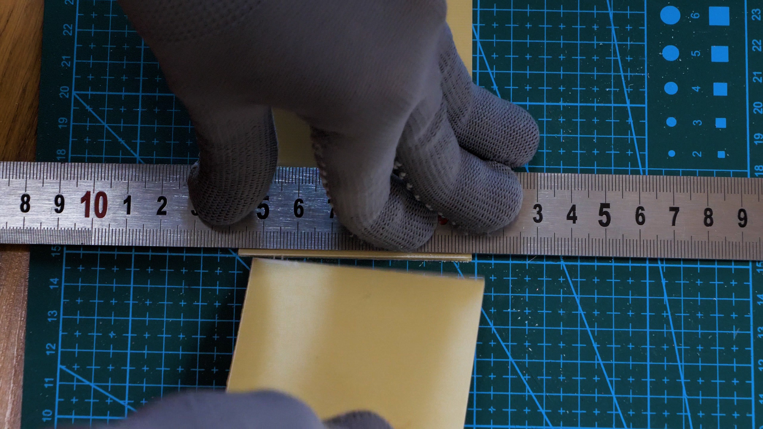
I cut the PCB by scoring it multiple times with knife and breaking it. Eye and respiratory protection should be used. I'm using CEM-1 copper laminate, which has less fiberglass than FR-4 and is pretty easy to work with.
![]()
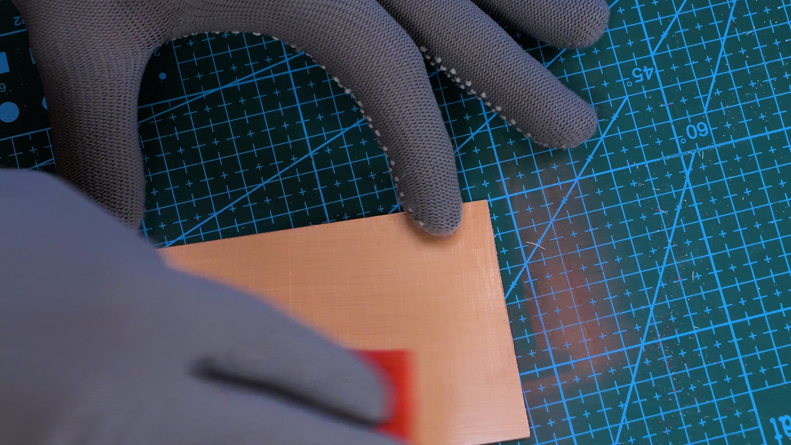
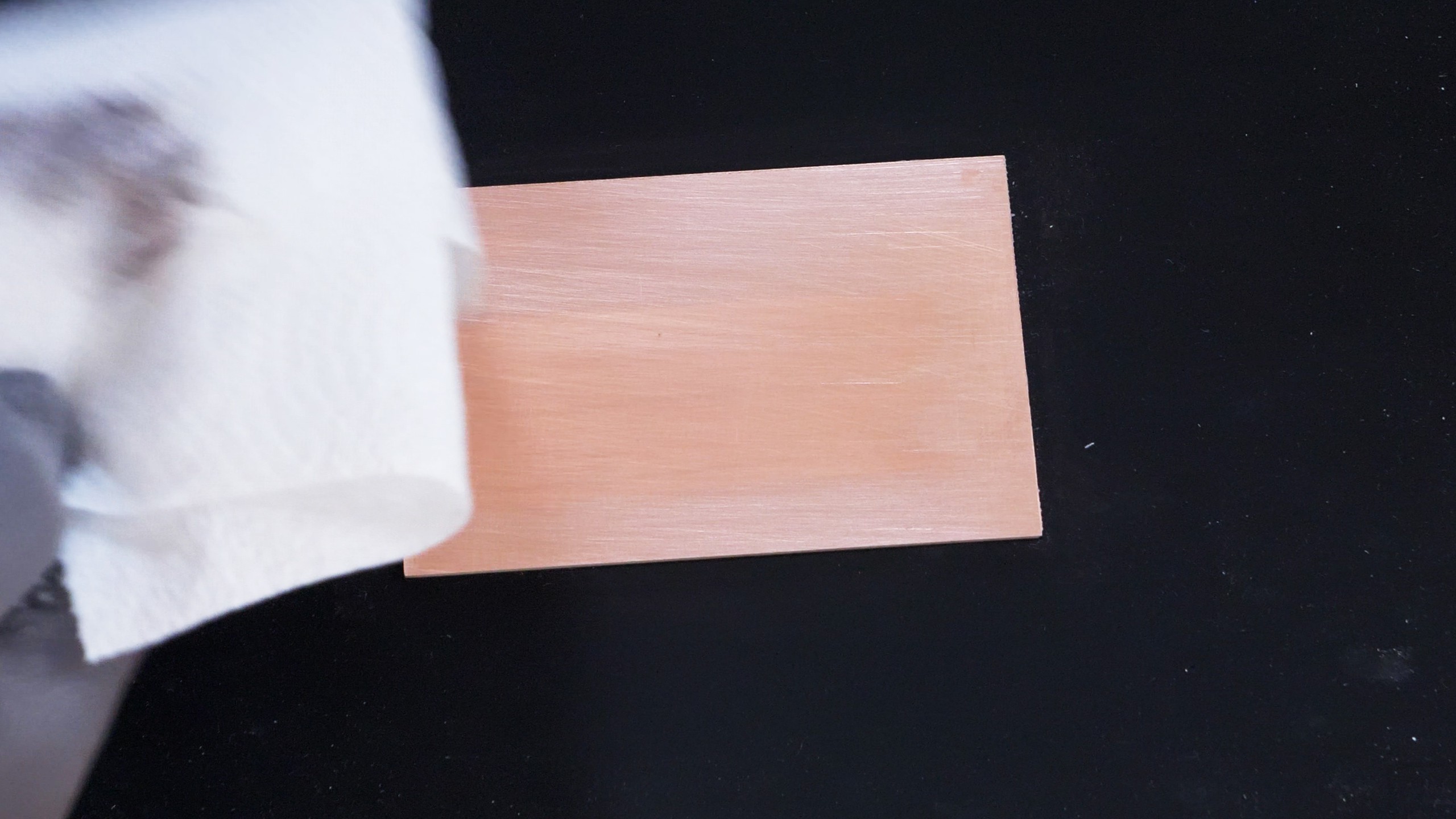
Now I clean the copper with abrasive material, and clean it further after that with some isopropyl alcohol.![]()
![]()
The board prepared in such a way is ready for next steps.
-
4Fitting the stencil
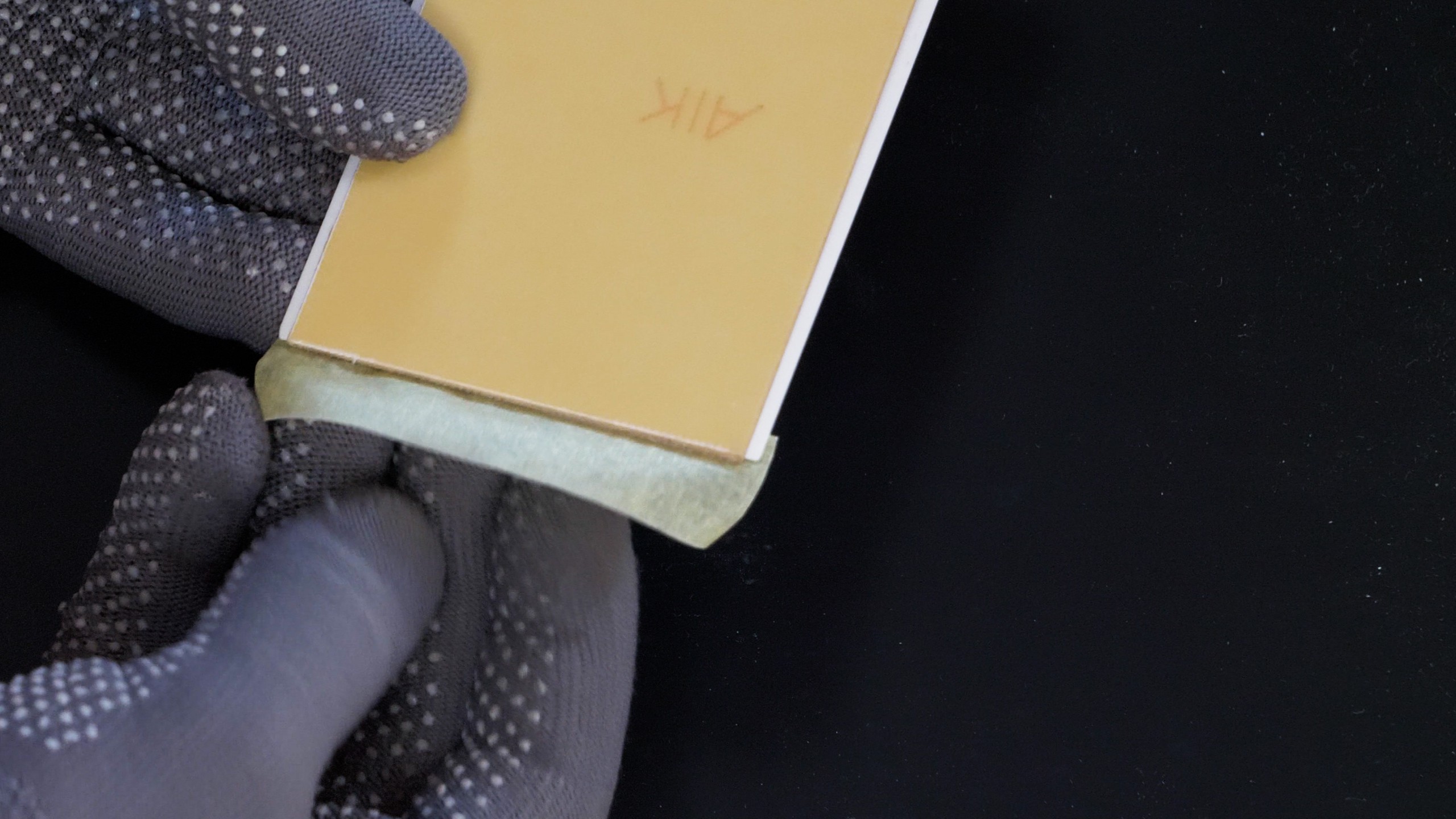
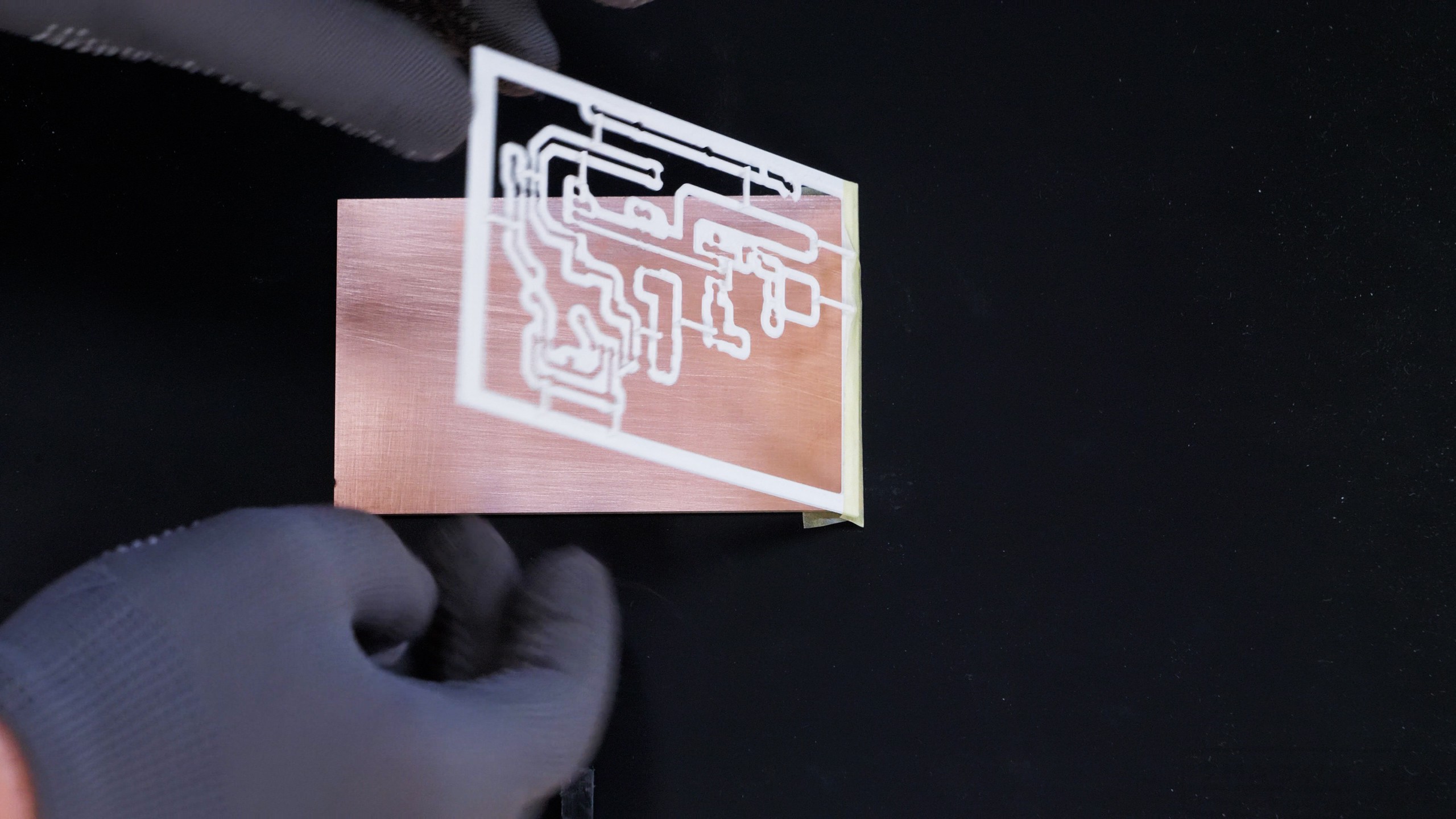
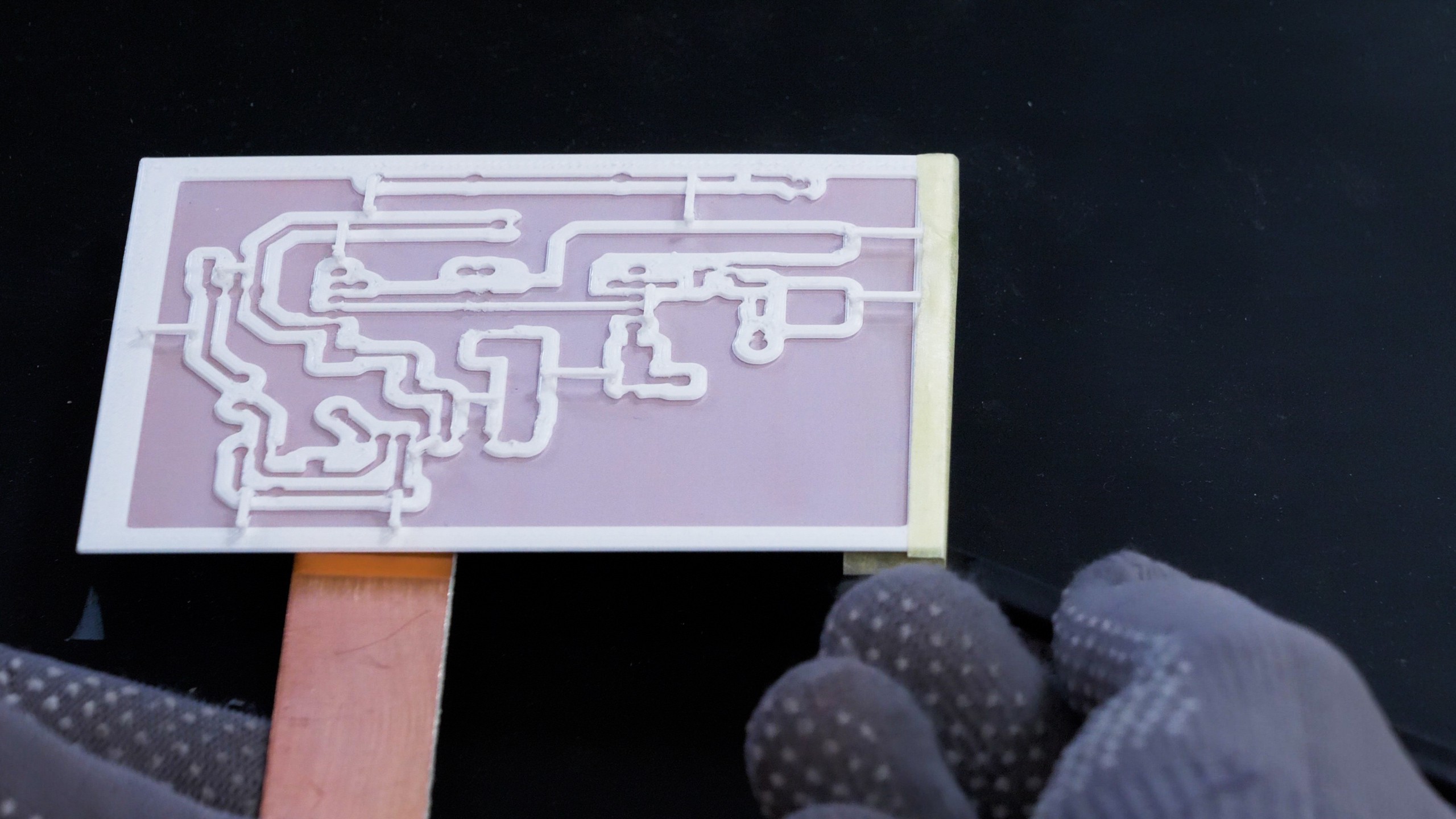
I place the stencil on the board and create a "hinge" using a piece of tape.
![]()
![]()
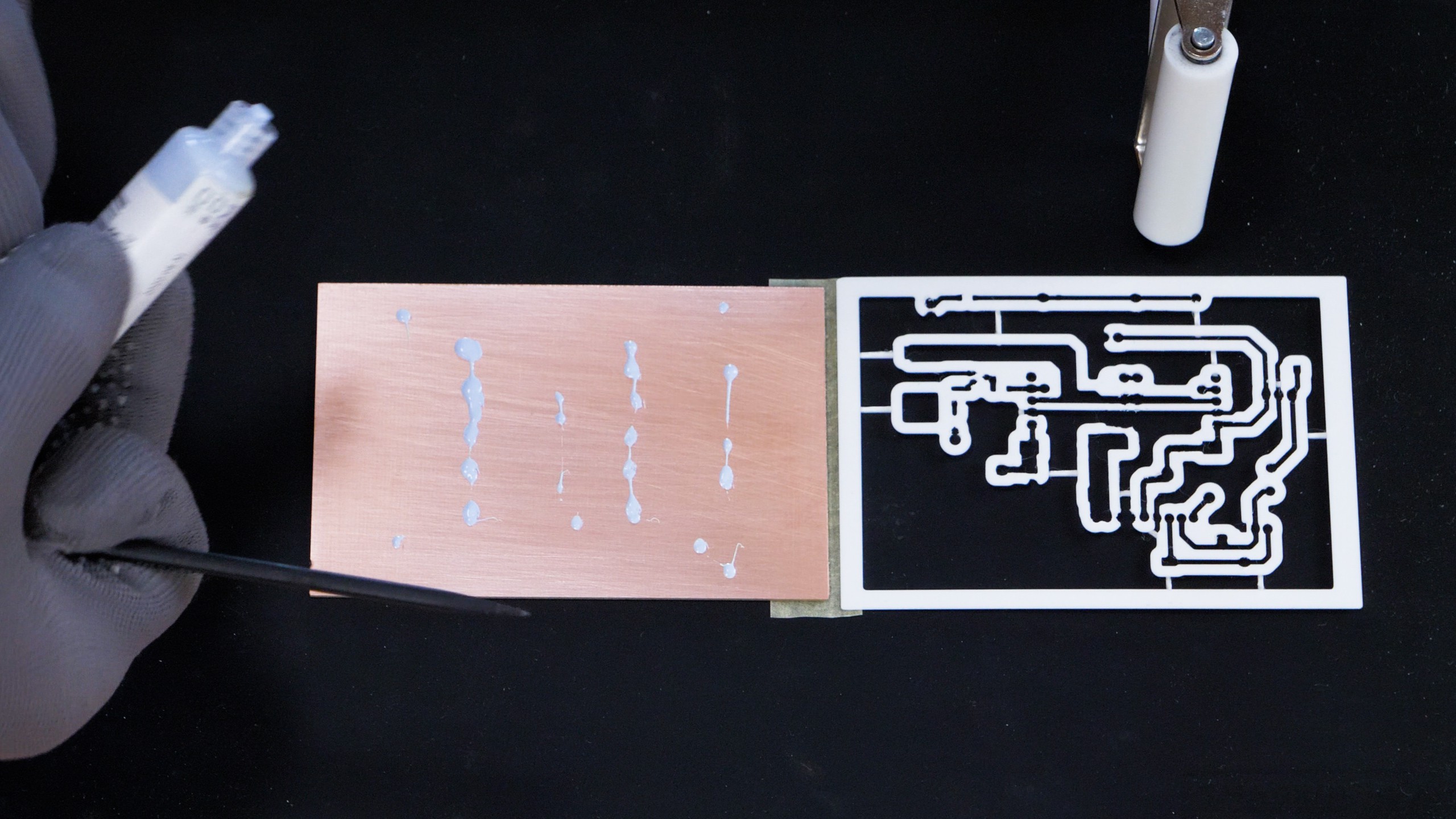
Now I open the "hinge" and lay the board and the stencil flat. I apply a bit of UV-curable mask.
![]()
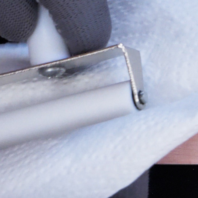
Now I clean the rubber roller with some alcohol and a piece of material that wouldn't leave too much fibers (paper towels may suffice)
![]()
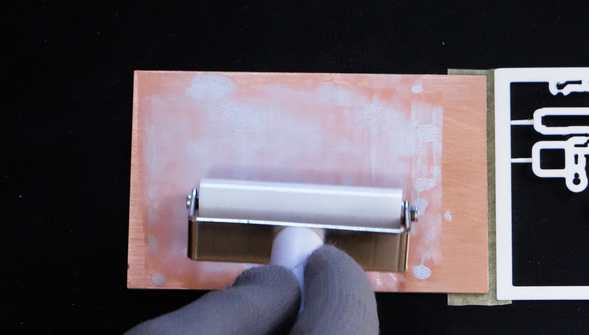
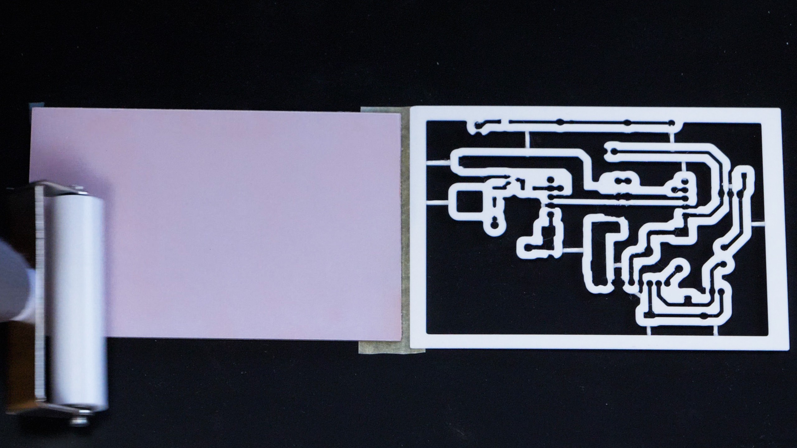
Now I spread the paint with rubber roller.
![]()
![]()
Now I carefully close the "hinge" and pick everything up, holding it from the bottom side.
![]()
-
5UV exposing and curing
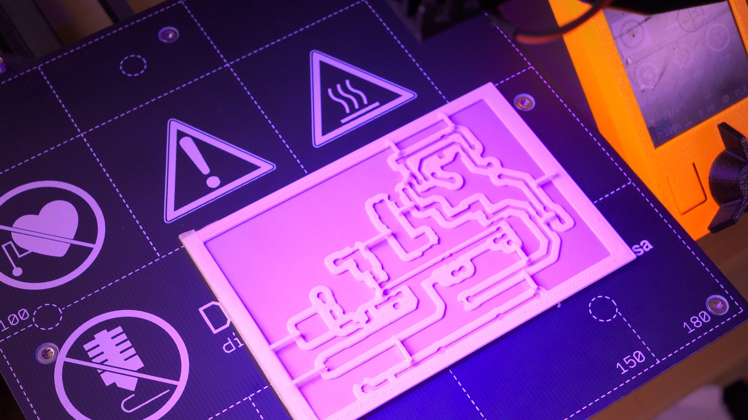
Now I'm going to expose the board under UV light. I'm going to place the board on a heated bed of a 3D printer, heated up to 58 degrees Celsius. That accelerates the curing process by a lot. Even higher temperature would be better, but it would cause warping of the stencil (I'm using PLA filament).
I mounted a 3-Watt UV LED around 20 centimeters above the heated bed.
![]()
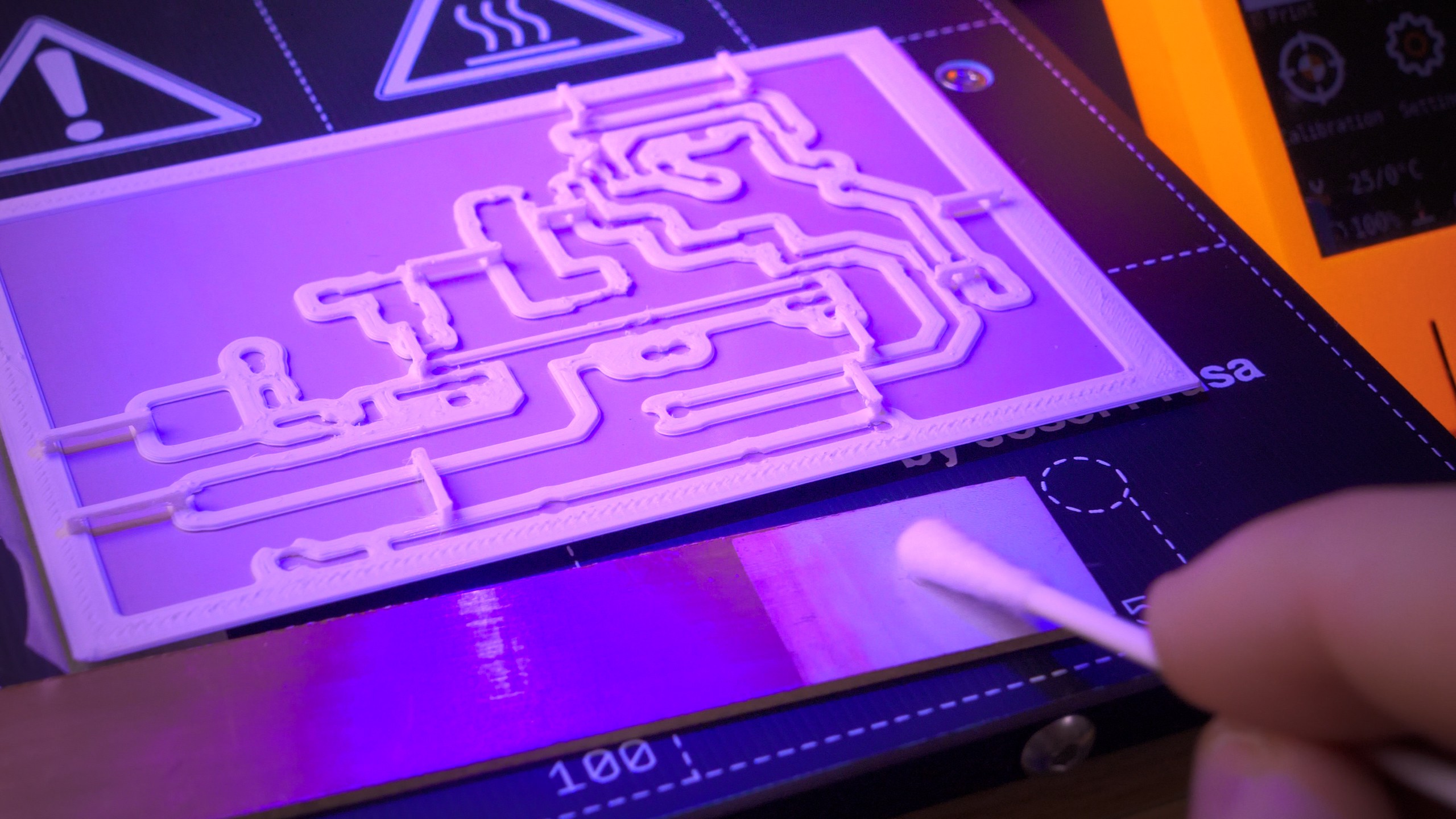
I also put a test piece with a bit of the UV mask on the heated bed. That way I can easily check if the mask has cured properly.
![]()
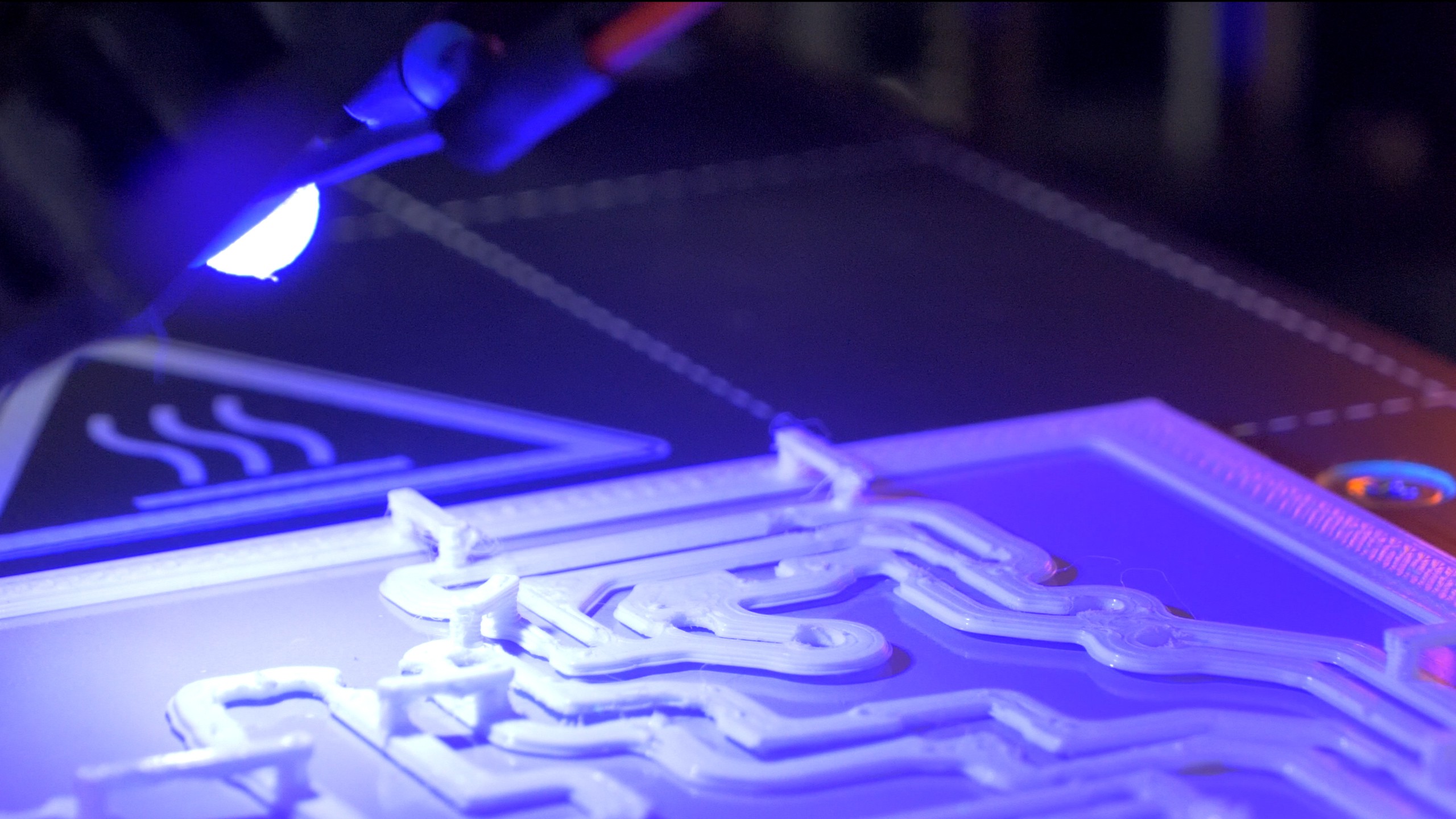
After the mask has been cured (around 5-10 minutes in my case), I apply UV light for additional 15 seconds to the area under each of the stencil "bridges".
![]()
Now the board should be exposed properly and ready for next steps.
-
6Cleaning the unexposed mask
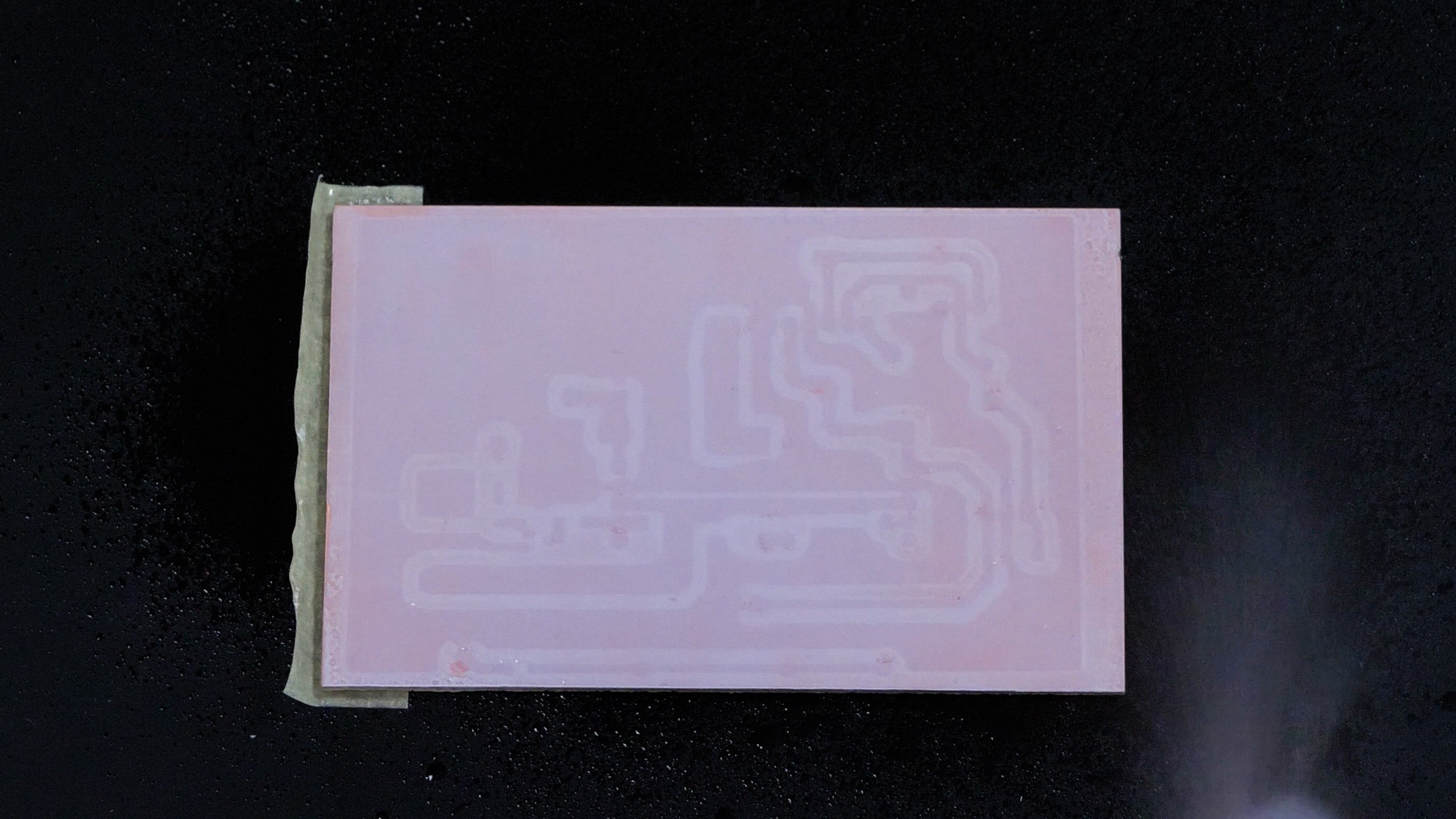
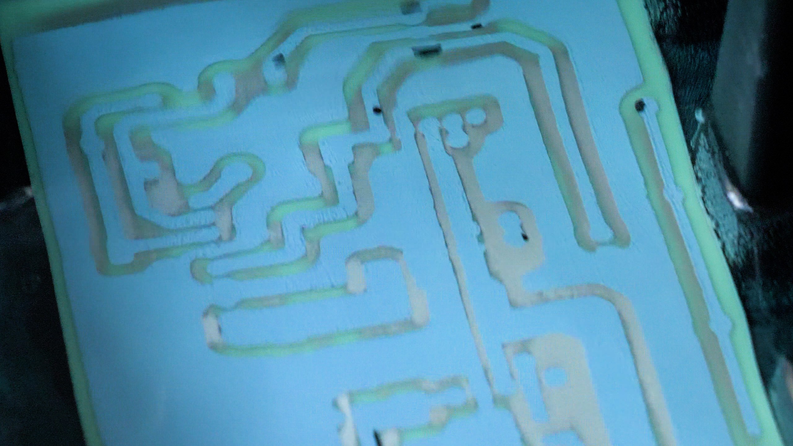
I removed the stencil and sprayed the board with isopropyl alcohol. The image of the PCB should appear right after spraying.
![]()
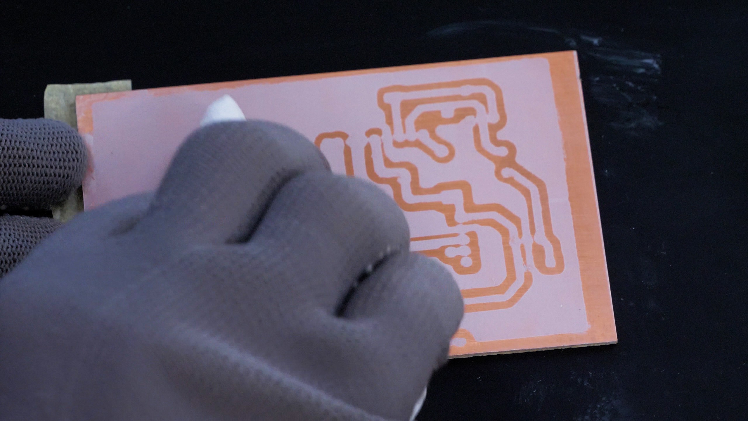
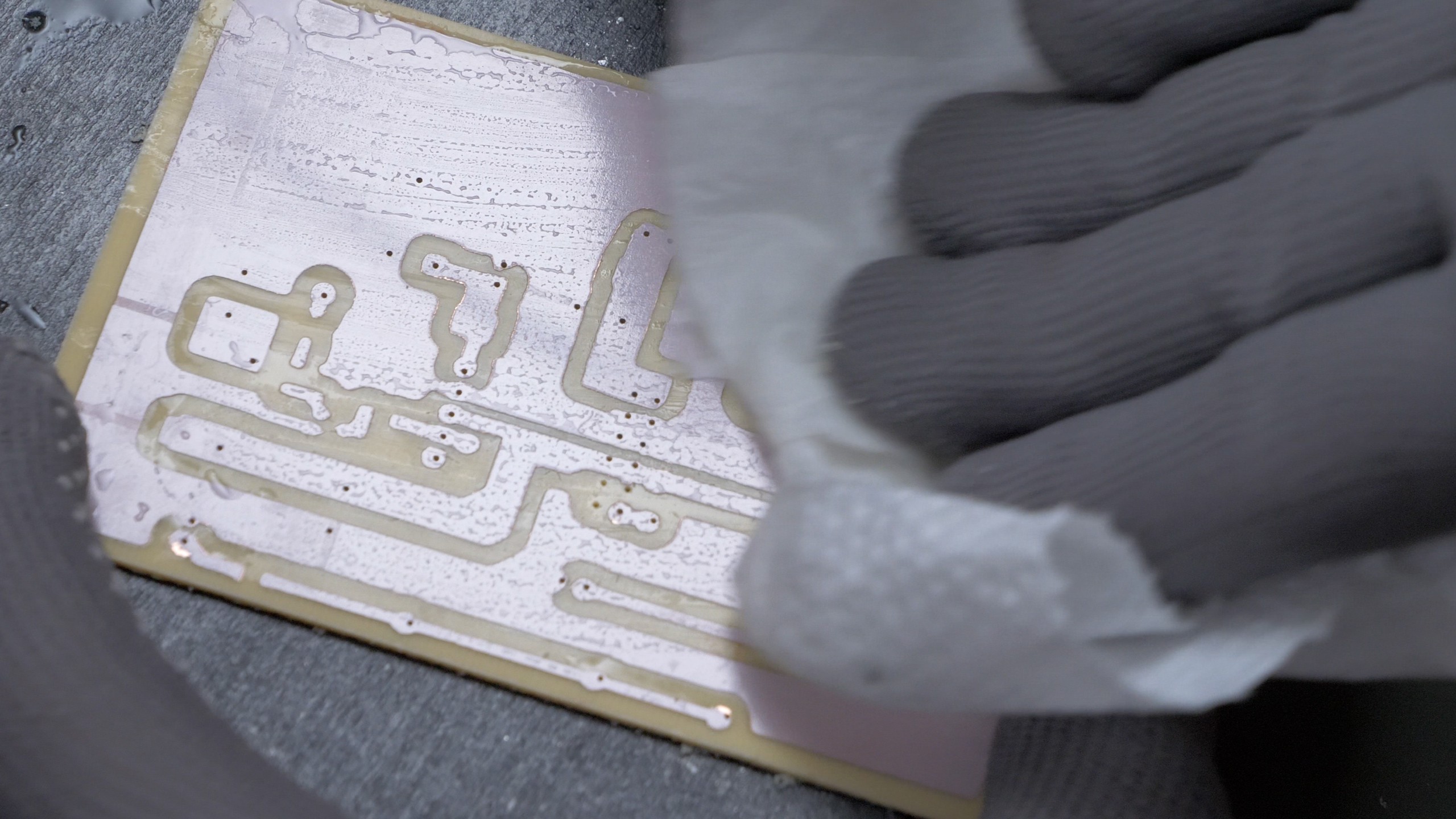
Now the board needs to be wiped with a paper towel.
![]()
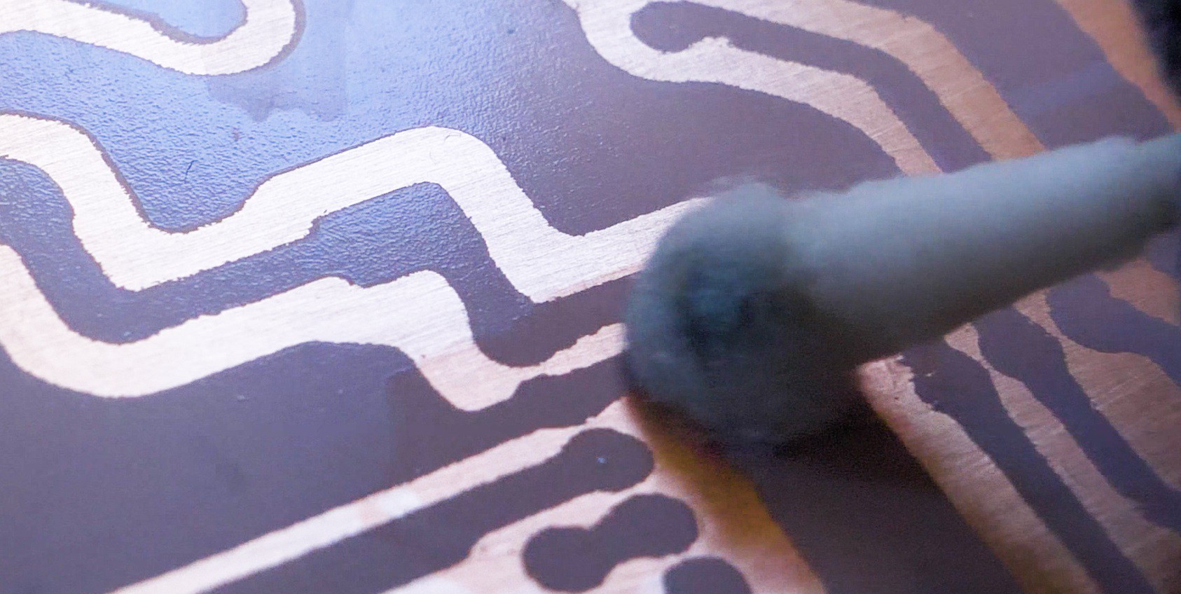
A bit of extra pressure may be required in some places.
![]()
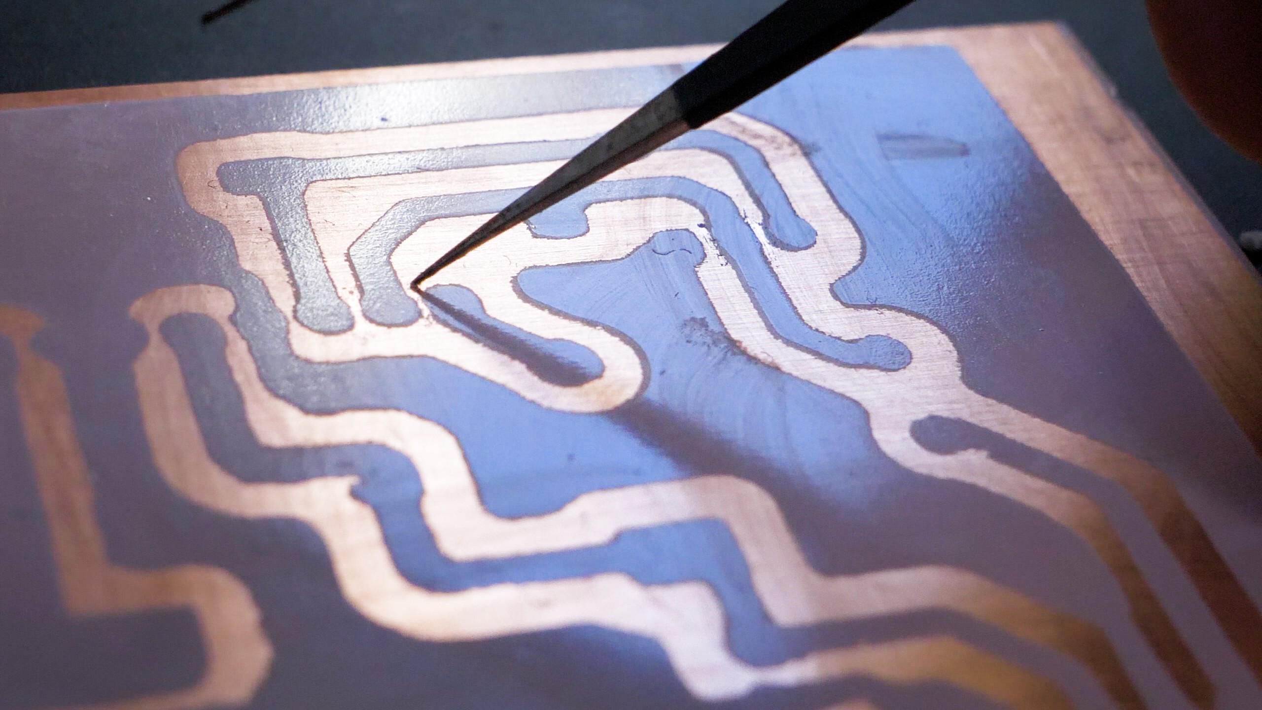
Any potential mask bridges may be removed using a sharp tool, i.e. with a tip of a tweezer.
![]()
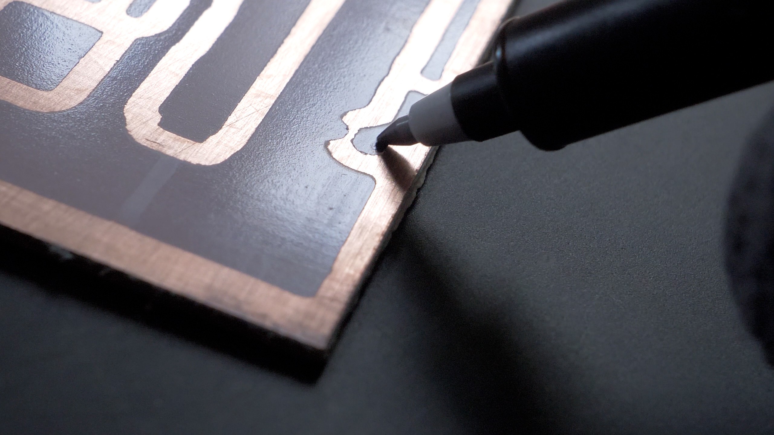
Any potential unexposed areas can be covered with a marker.![]()
Now the board is ready for etching. -
7Etching
Etch the board using a suitable etching solution. I'm using sodium peroxide. Follow all the necessary safety precautions and instructions. There are different etching solutions available and multitude of available tutorials, so I'm not going to cover this step in detail. Be sure to store the solution in a suitable container afterwards for later reuse, or for a proper disposal.
Sodium peroxide requires some heat and stirring to accelerate the process, therefore I placed the container with etchant on a heated bed of the 3D printer and programmed some motion for stirring the solution.
![]()
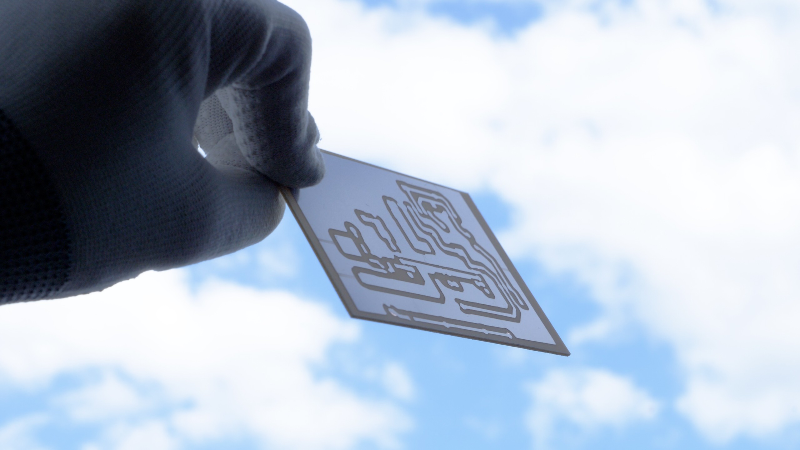
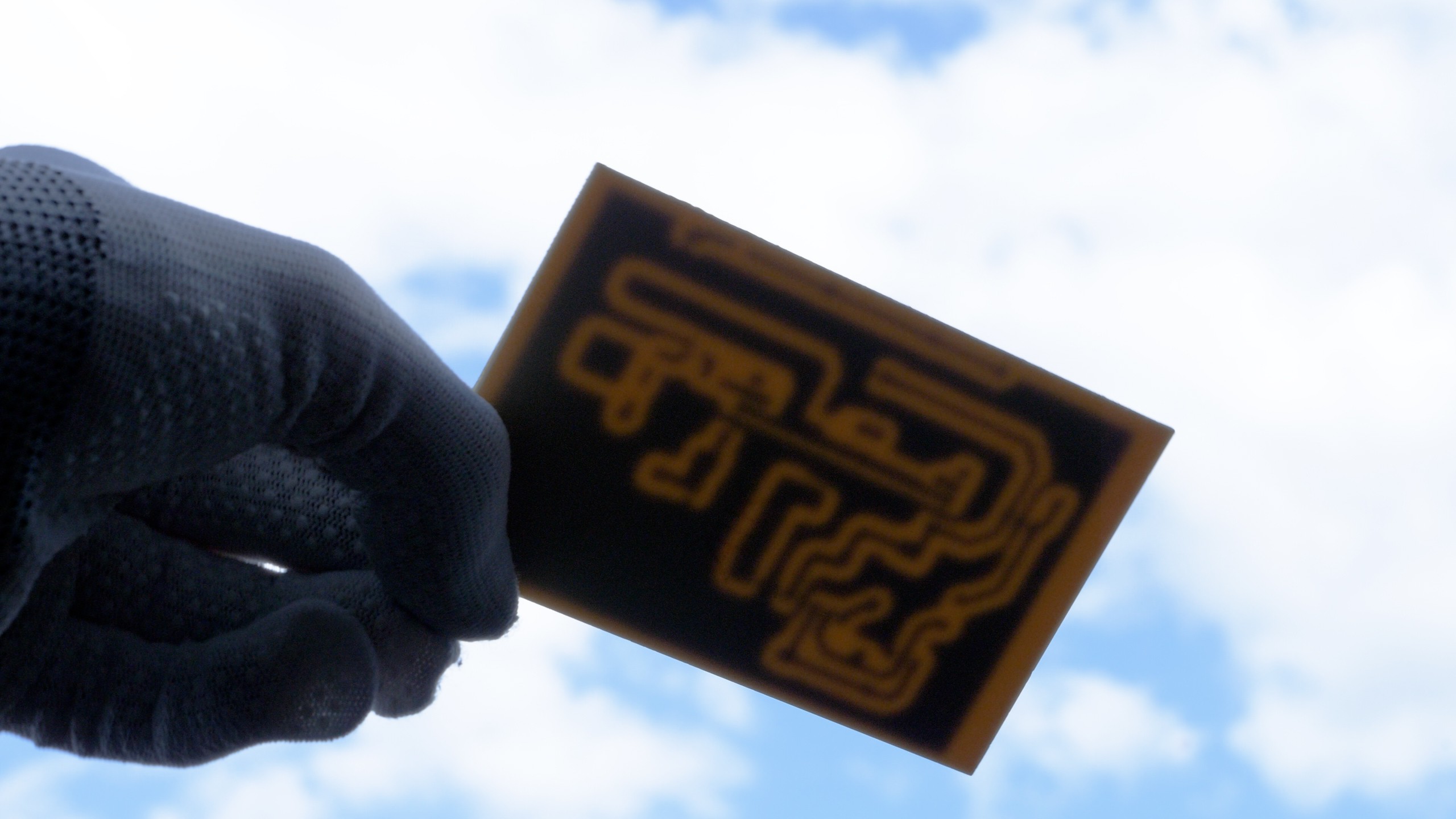
This is how an etched, cleaned and rinsed PCB should look like:
![]()
![]()
I removed the dark spots from the marker with some isopropyl alcohol. The soldermask is still attached to the board and will need to be removed from the solder pads.Now the board is ready for the last steps of the process.
-
8Drilling (optional)
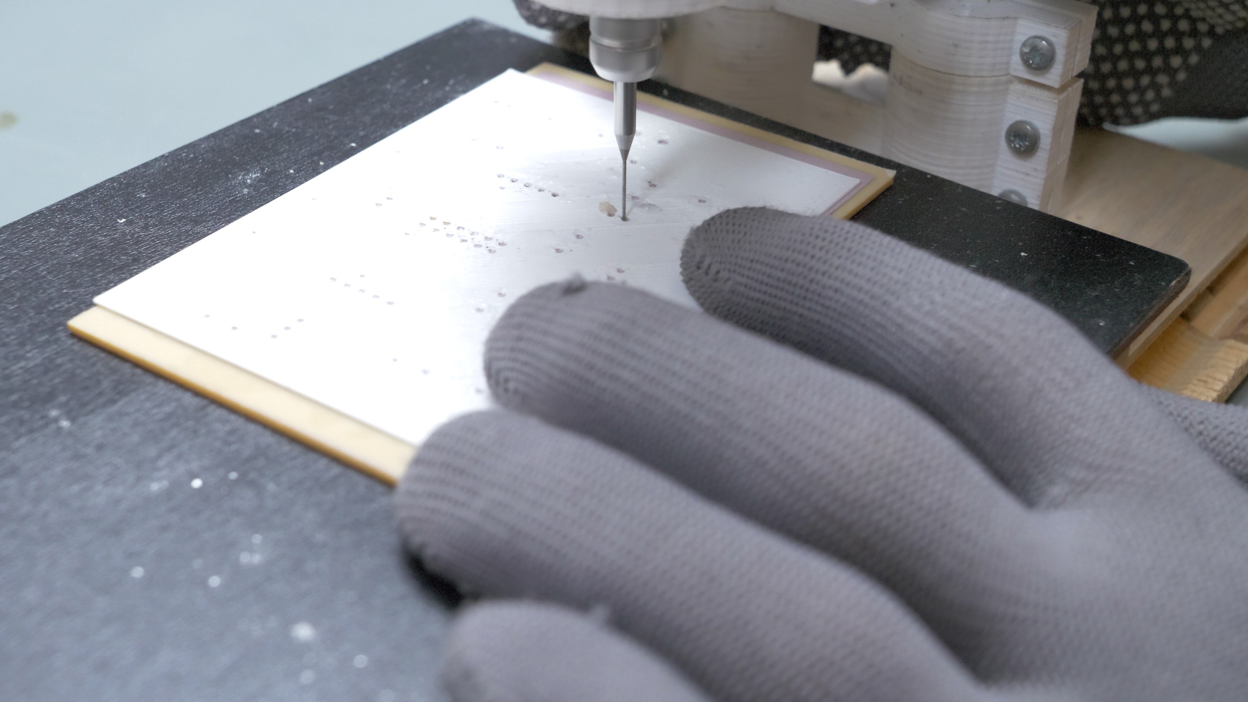
If there are any through-hole components, the board needs to be drilled. I'm using a 3D-printed drill guide and tungsten carbide drill bits. Be sure to use eye and respiratory protection.
![]()
I sprayed the board with water before drilling to minimize the dust.
![]()
Now the board is almost ready.
-
9Remove the mask from solder pads
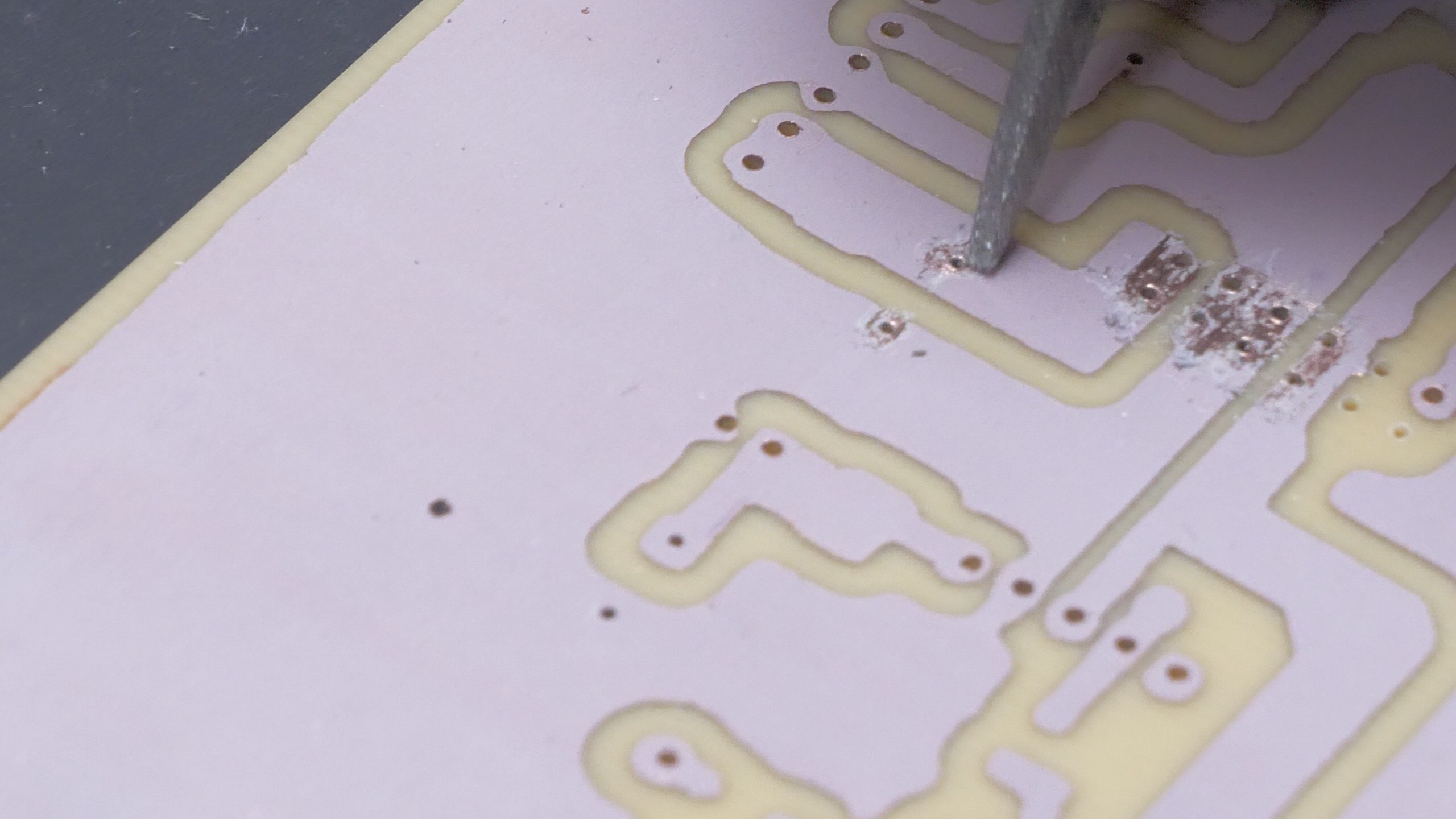
I scraped the mask away from solder pads using a diamond file. Any sharp tool should work - the mask is resistant to rubbing away, but it's pretty easy to scrape it away.
![]()
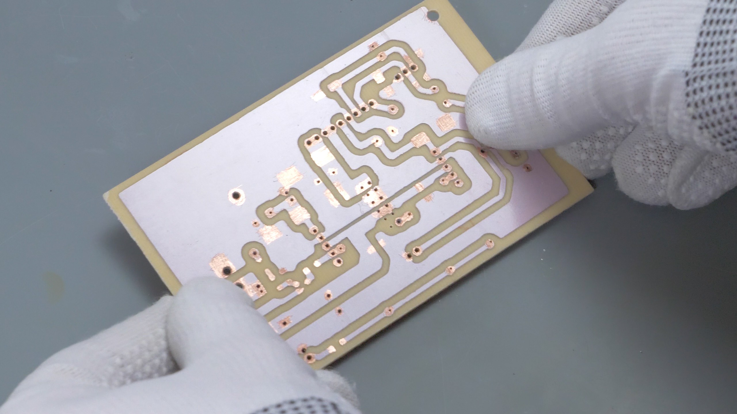
Now the board is ready for assembly and soldering:
![]()
![]()
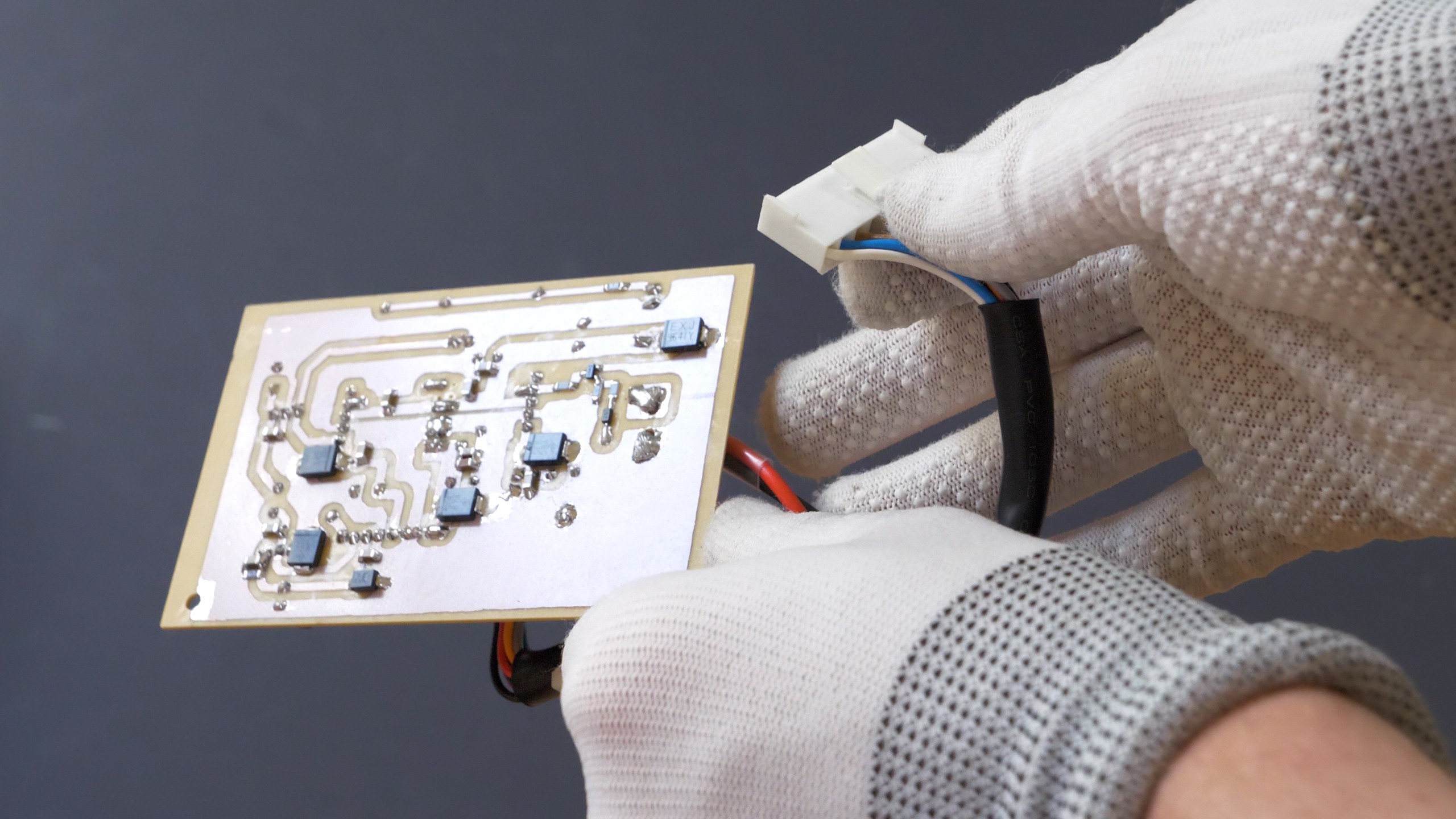
I used this PCB for a replacement power supply for a vintage computer in this project: https://hackaday.io/project/186447-toshiba-t3200sxc-fixupgrade-new-psu-lcd-wifi
Making PCBs with 3D printed stencil and UV paint
A different way of making PCBs with a rubber roller, UV-soldermask paint as etching mask and 3D printer

Discussions
Become a Hackaday.io Member
Create an account to leave a comment. Already have an account? Log In.