-
lots of macros
09/23/2022 at 20:35 • 0 commentsWhen I started this, I didn't realize how many macros I would have to write to just get the VGA tested. Like increment, then add 8 bit numbers, decrement, subtract 8 bit numbers, shift left 8-bits, shift left on 16 bit numbers, I need to make a stack with push and pop, and then subroutine jump and return macros.
In order to help all of those, I'm using the Basys3 board which has 16 switches and LEDs, and a 4-digit seven-segment display, and a serial interface. So I made peripherals for those with registers to read/write.
It's slow going but when even doing a simple shift-left is an exercise, it takes a long time. But it has to be faster than doing it on a breadboard.
-
mov or cpy?
08/24/2022 at 19:38 • 1 commentI realized that the one instruction isn't really a move. It's more of a copy. The original value isn't destroyed in the process. I'm not sure why I didn't realize this until now. Don't think I'll change anything. Just an interesting note.
-
Python assembler
08/22/2022 at 18:33 • 0 commentsI believe I've finished the VGA part of the design. I've had to capture two pixels per address since it toggles back and forth between VGA and CPU. So it only uses half the amount of memory now, but I dropped it to only 3-bit color. I store the vsync and hsync in RAM to minimize logic as well. I need to write a program to load the right sync values in the right locations in order to test the VGA. For that, I need to do some coding for the CPU.
In order to do some coding, I really need a decent assembler. I decided to take a page from the Gigatron and use Python as my assembler. I looked around for a customizable assembler, but this assembly is a little different from most in that it doesn't have instructions to code - just addresses. So I wrote my own. It's probably my least-favorite part of the project. I have it assembling into hex now, but I'd like to have it output into native VHDL so I can easily integrate it into my FPGA and run it. At least I brushed up on my Python skills.
-
VGA generation
08/02/2022 at 20:11 • 0 commentsMy plan for VGA generation is to use simple counters for the VGA timing. It will access the RAM like a raster memory with the sync signals stored in each byte. Nothing new. I want only one RAM for both video and processor, so my plan is to just toggle access. Video gets it for one clock and processor gets it for one clock. That shouldn't be a problem for blanking - it may shrink the usable video area for a couple rows/columns. That reduces RAM available for the processor. I think 160x120 is ok - that's 19,200 bytes of the RAM or 59%. There won't be video until the processor initializes it with the syncs and blanking, but it's a good test to see if the processor is working correctly.
-
CPU operation
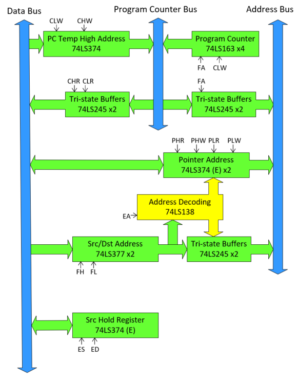
08/02/2022 at 16:42 • 0 commentsI want to add a quick note for operation of the CPU.
The CPU only does move instructions. So each instruction is a source address and a destination address. The memory map of the processor is simple:
Address: Function
0: Trash register. Write to this to send the data nowhere
1: Program counter (Lo byte). Read or write to this address to update the program counter
3: Program counter (Hi byte). Read from this normally. Writing here will write to a temporary holding register. When the Lo byte is written to, the high byte is transferred from the temporary register to the high byte of the program counter.
5: Pointer address (Lo byte): Write-only to the address pointer. When the pointer data register is Read/Written, the pointer address is used instead.
7: Pointer address (Hi byte): Write-only to the address pointer. When the pointer data register is Read/Written, the pointer address is used instead.
8: Pointer data: Read/Write register. When this address is written or read, the data will instead go to/from the address stored in the pointer address registers.
And that's it for the CPU instructions. The ROM and RAM and all other peripherals can go anywhere else. However, the program counter starts up at zero. So it will execute a few garbage commands first. I use the ROM at $0000-$7FFF, and the RAM at $8000-$FFFF. The CPU will go into the ROM boot code then after reset. The CPU has an override signal that goes to the ROM to prevent it from outputting to the data bus when the $00-$0F functions are accessed by the CPU. This can also be used by other peripherals if you put them in the lower memory space. I may change this so that the CPU functions are at like $FF00 instead so it can boot right into ROM. I figure I'll sort it out after the video is done.
The CPU can do simple arithmetic using the ROM and indirect addressing, or branching using indirect addressing as well. Or you could add an ALU peripheral if you want.
-
CPU redevelopment
08/02/2022 at 14:39 • 0 commentsI will first focus on redesigning the CPU. I don't think the design will change much from a high block level, but most of the chips will be different. I had to make a couple compromises like I'm gating the clock to some of the 74LS374 which is a digital no-no. The datapath now requires 17 chips - definitely more than you'd need for a simple CPU.
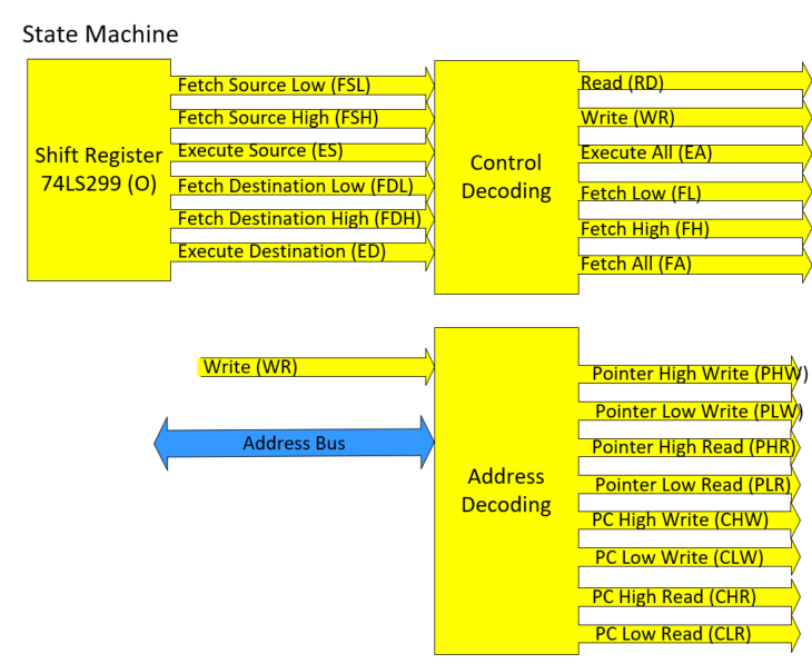
The state machine is just a shift-register. Six clocks are required for every instruction. Each instruction is 4 bytes - two bytes for a source address and two bytes for a destination address. That's 4 fetches from memory, and then 1 to execute the read The reset of the decoding is a 74LS138 and 4 chips for the AND and NOT gates.
I believe that brings us up to 22 chips for the CPU. And that's not counting how many will be needed for the VGA. Not great, but there's no microcode. I like to use the project by roelh and his 1inch square CPU ( https://hackaday.io/project/161251-1-square-inch-ttl-cpu ) with 8 chips. However, there's a giant flash ROM, so if you go by transistor count it's quite high compared to this one. And the Gigatron combines the CPU and VGA into one, so that will definitely have less too. I'm going to try to make the VGA circuit so that you could pop out this CPU and put whichever one you'd want in its place.
One instruction VGA computer
Incorporates an improved minimal-chip One Instruction CPU with a hardware-driven VGA output