 micl
micl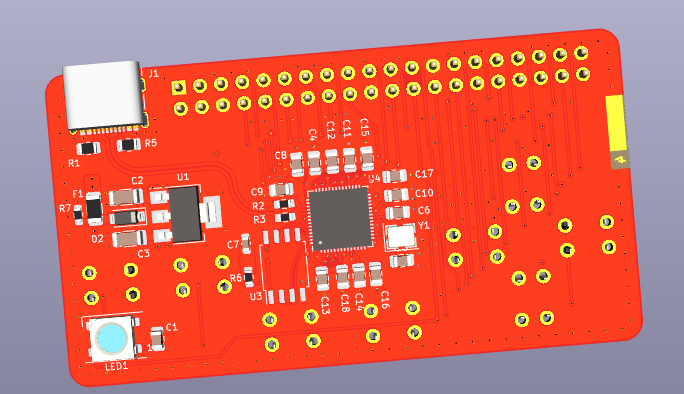
I don't think this design is ready for production, I had a go at Manhattan routing on the top and bottom layers for the majority of the signal traces, because I intend to run the board at a clock rate >400MHz as a demonstration of how much the RP2040 can handle... but it resulted in an excessive via density. To avoid cutting up ground repeatedly, I had to insert vias everywhere between parallel traces.
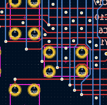
I agree, it's kind of hideous. The gridding is probably going to cause coupling when the traces transfer from referencing ground, to referencing power, so for the next iteration my goal is to simplify and clean up my routing to both minimize the length of each trace, as well as improve the noise immunity of the board without heavy crosstalk.
Generally though, I think the board has made some progress.
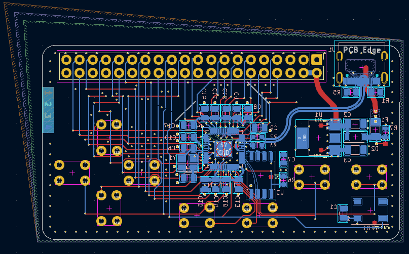
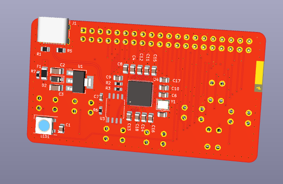
I don't think a gridded layout serves any particular advantages for the design (it was recommended to me on a forum somewhere), and it substantially increases the via count. I'm probably going to just delete all of the GPIO traces and do it the regular way, but bus as many of the lines together as I can to avoid cutting up the ground plane everywhere.
Discussions
Become a Hackaday.io Member
Create an account to leave a comment. Already have an account? Log In.