* * OVERVIEW * *
Studio 68 is a board to make retro-computing "experiments".
It has a 68SEC000 CPU, a STM32F030R8T6 MCU + USB + SD, a 16MWord SDR DRAM and a 208pin FPGA. So It is possible use an approach based on virtual HW emulated using the STM32 MCU or synthesized inside the FPGA (or a mix of both).
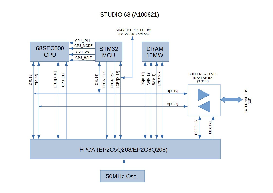
Here the Block Diagram of the Studio 68: there are two main connectors, the GPIO and the EB (External Bus).
The (SHARED) GPIO allows to use little add-on boards/adapters as the one to give a VGA/KB output (the VGA/KB core must be implemented inside the FPGA).
The EB is an external bus. It allows to add a board for virtually any CPU to make experiments and emulate peripherals HW inside the FPGA:
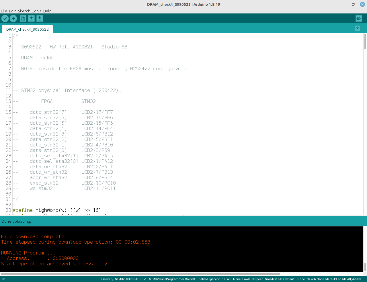
The STM32 part of the Studio 68 board is compatible with the Discovery development board by ST with the same STM32 MCU (32F0308DISCOVERY), so it is possible use Arduino IDE (with the ST core) as quick development environment selecting the Discovery as target board and the serial upload mode (the Studio 68 has a circuitry to use the STM32 embedded serial bootloader with Arduino IDE to enable "automatic" uploads):
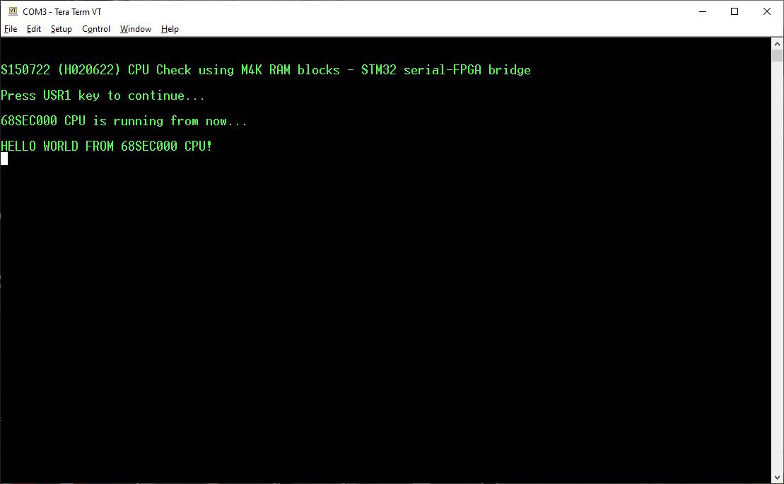
Here a test running on the onboard 68SEC000 CPU using a test VHDL to implement some RAM and the needed I/O registers to handle a serial port (the serial port is physically implemented with the STM32 that exchanges data with the I/O registers inside the FPGA):
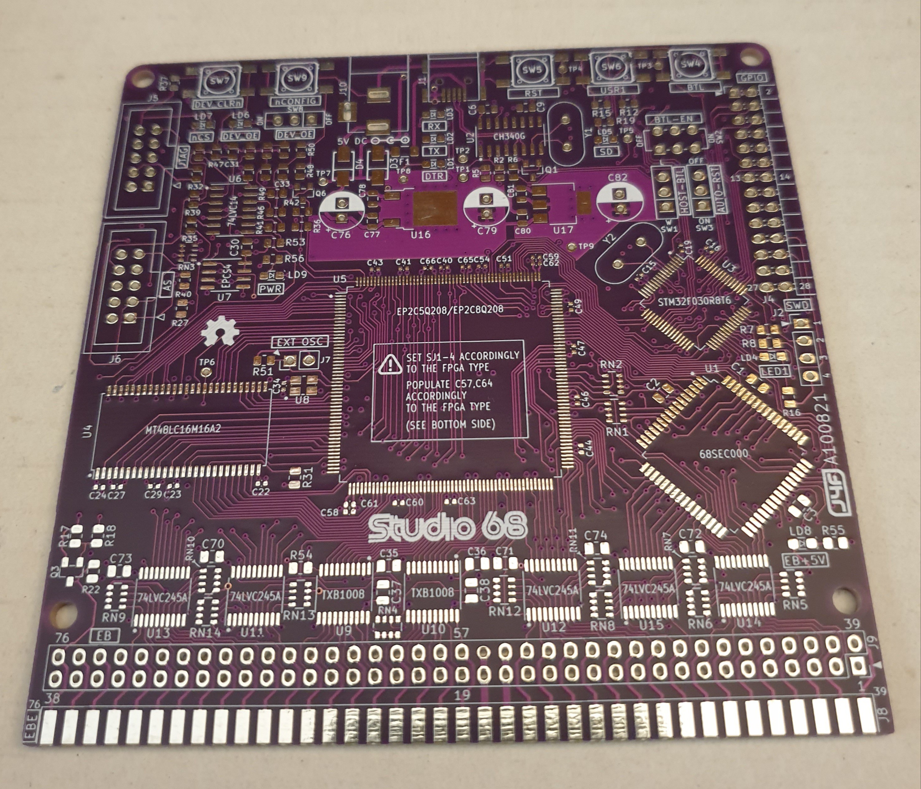
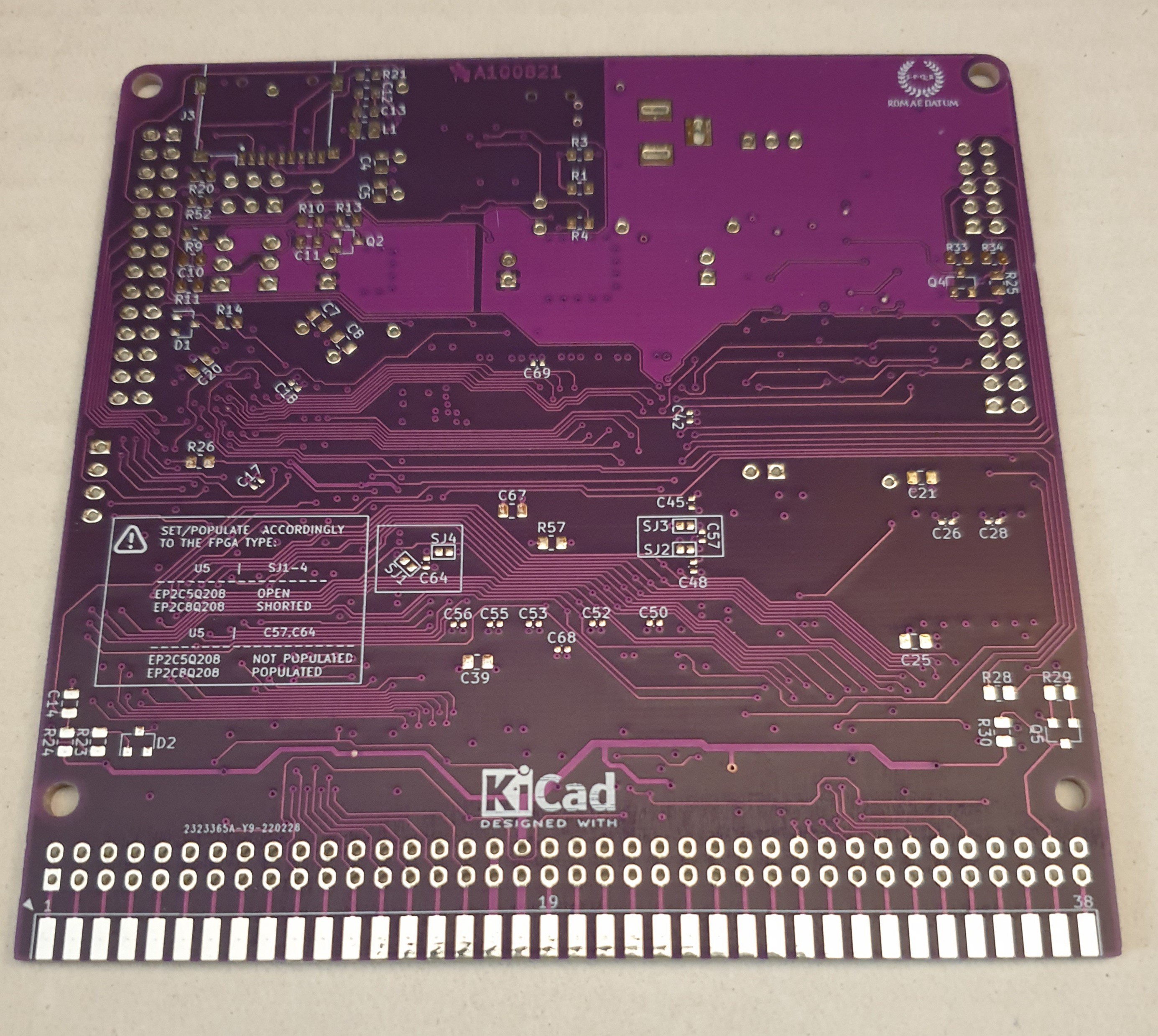
The 4-layers PCB of the Studio 68:
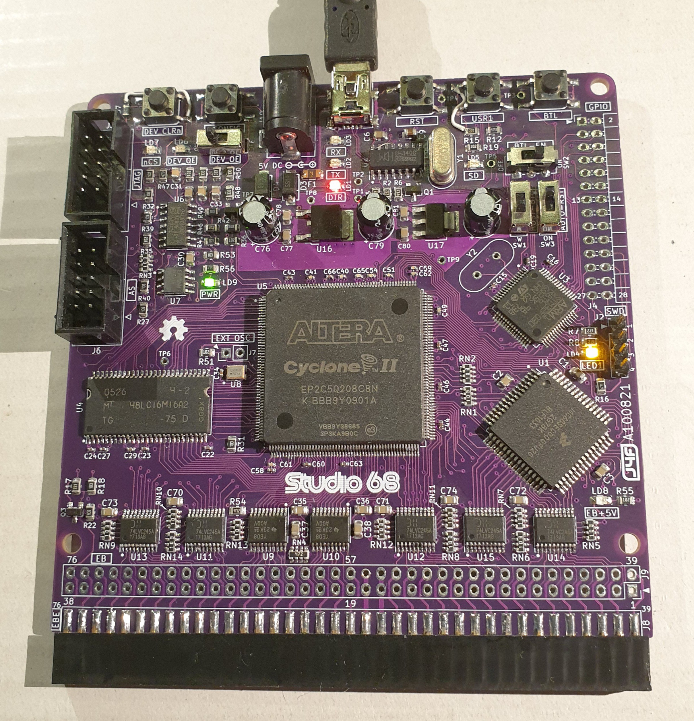
The board (almost) assembled:
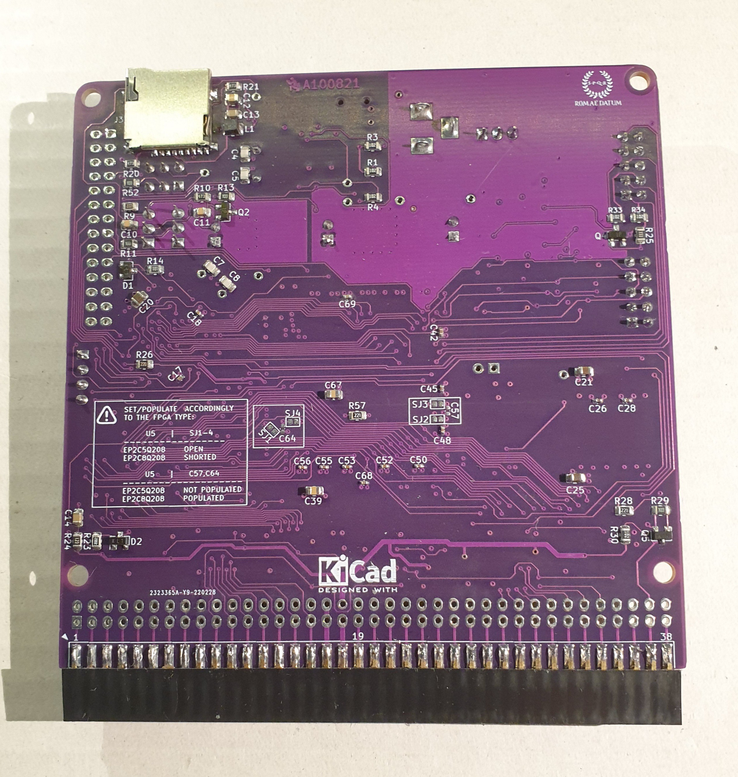
* * PROJECT STATUS * *
The Studio 68 board is currently under development/testing.
Current related boards (by HW reference code):
- A100821: Studio 68
- A100821-R080422: Studio 68 (first public release - design revision stage)
- A291221: KR1801VM2 Application Board
- A050922: KR1801VM2 Blinking Leds
- A190922: Z80 Application Board
- A220922: Z80 Blinking Leds
- A031022: VGA Adapter
All the documentation needed to build the boards (schematics, gerber, etc.) will be published when ready.
* * Z80 CPU (T84C00AM) APPLICATION BOARD * *
Thanks to PCBWay that kindly offered me to produce this new beautiful 4-layer PCB, I've done a Z80 Application Board (APB) to try out this CPU (T84C00AM) with the Studio 68 board:
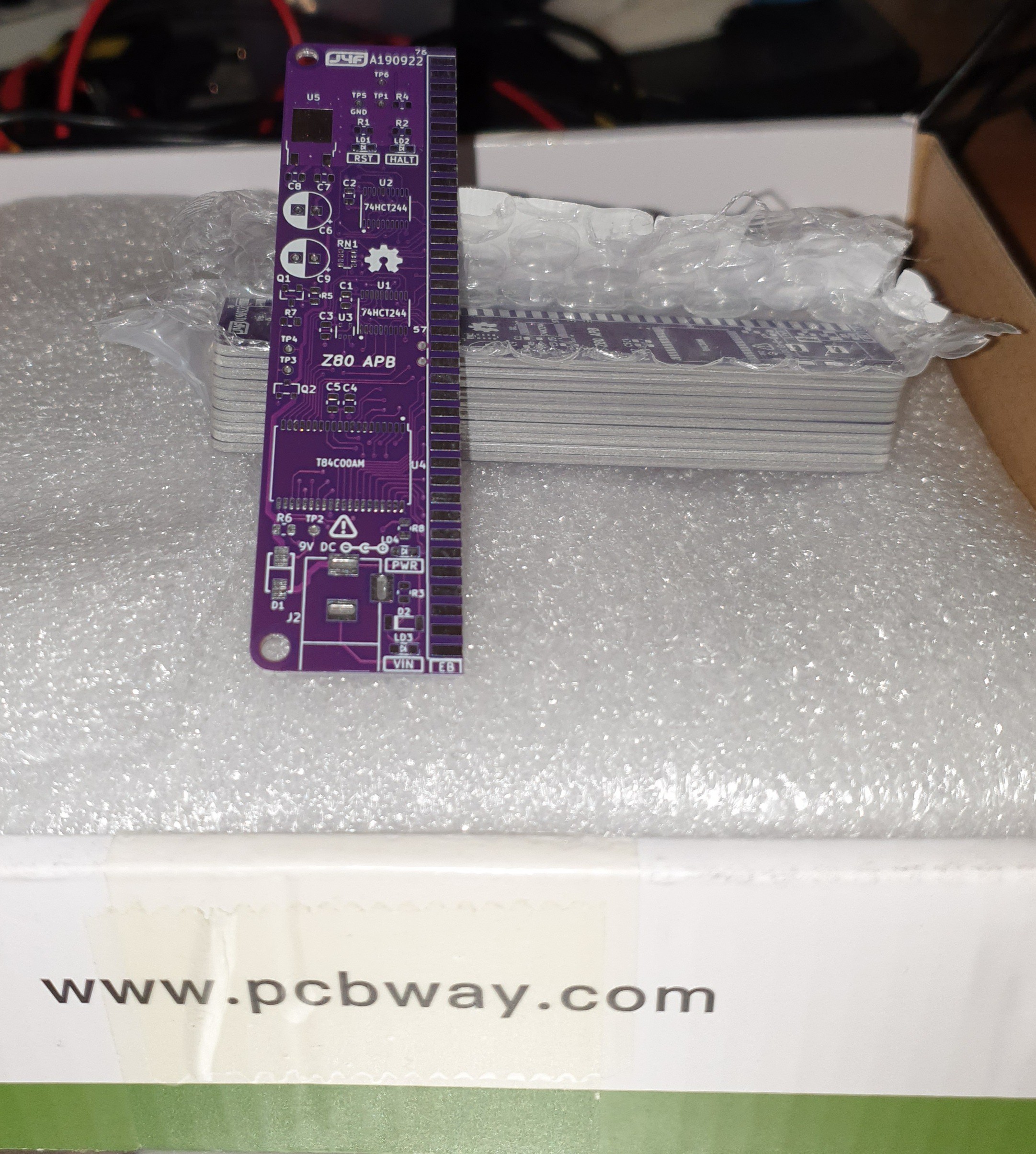
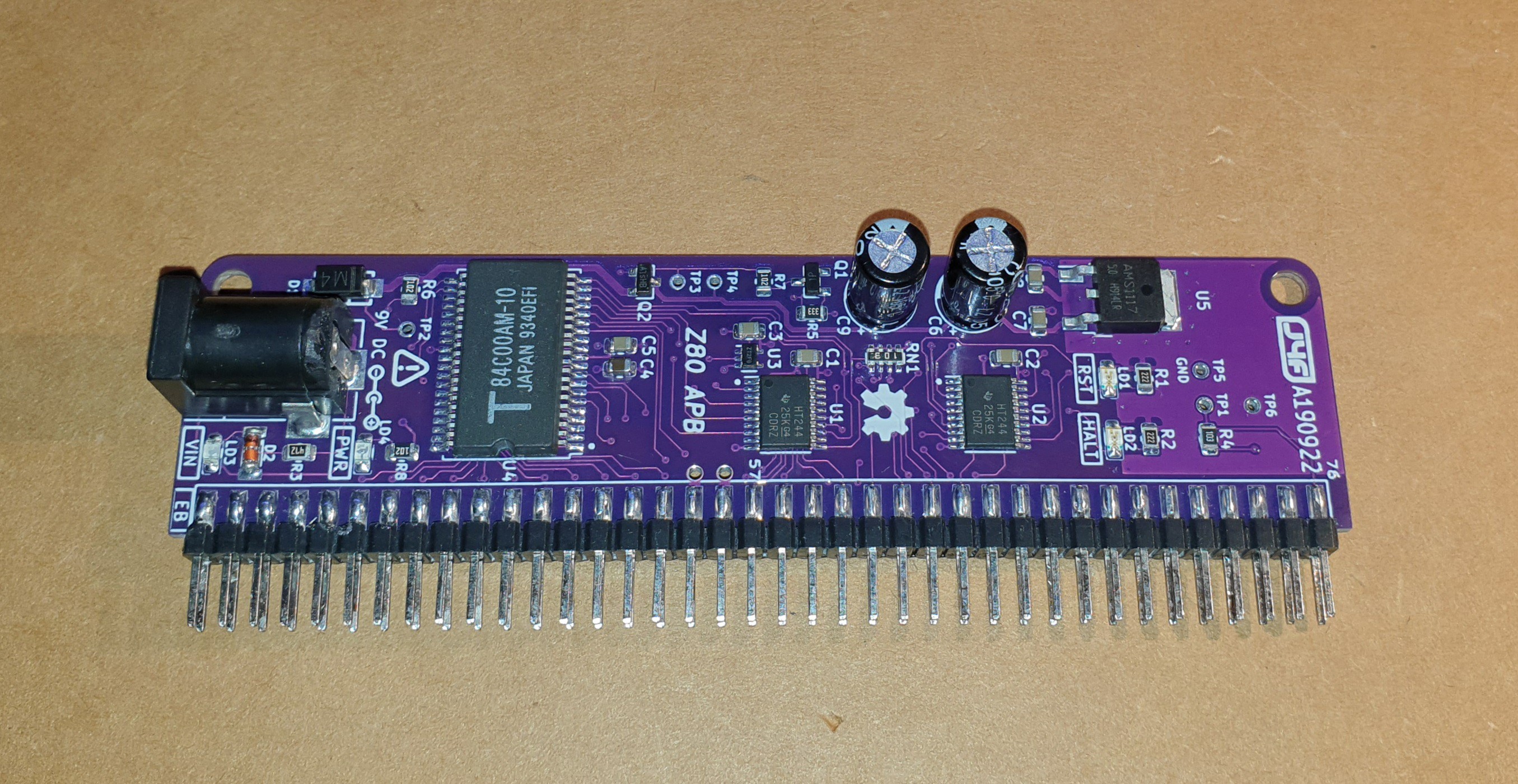
It is a self-powered board as Studio 68 doesn't power what is connected to the external bus (EB/EBE).
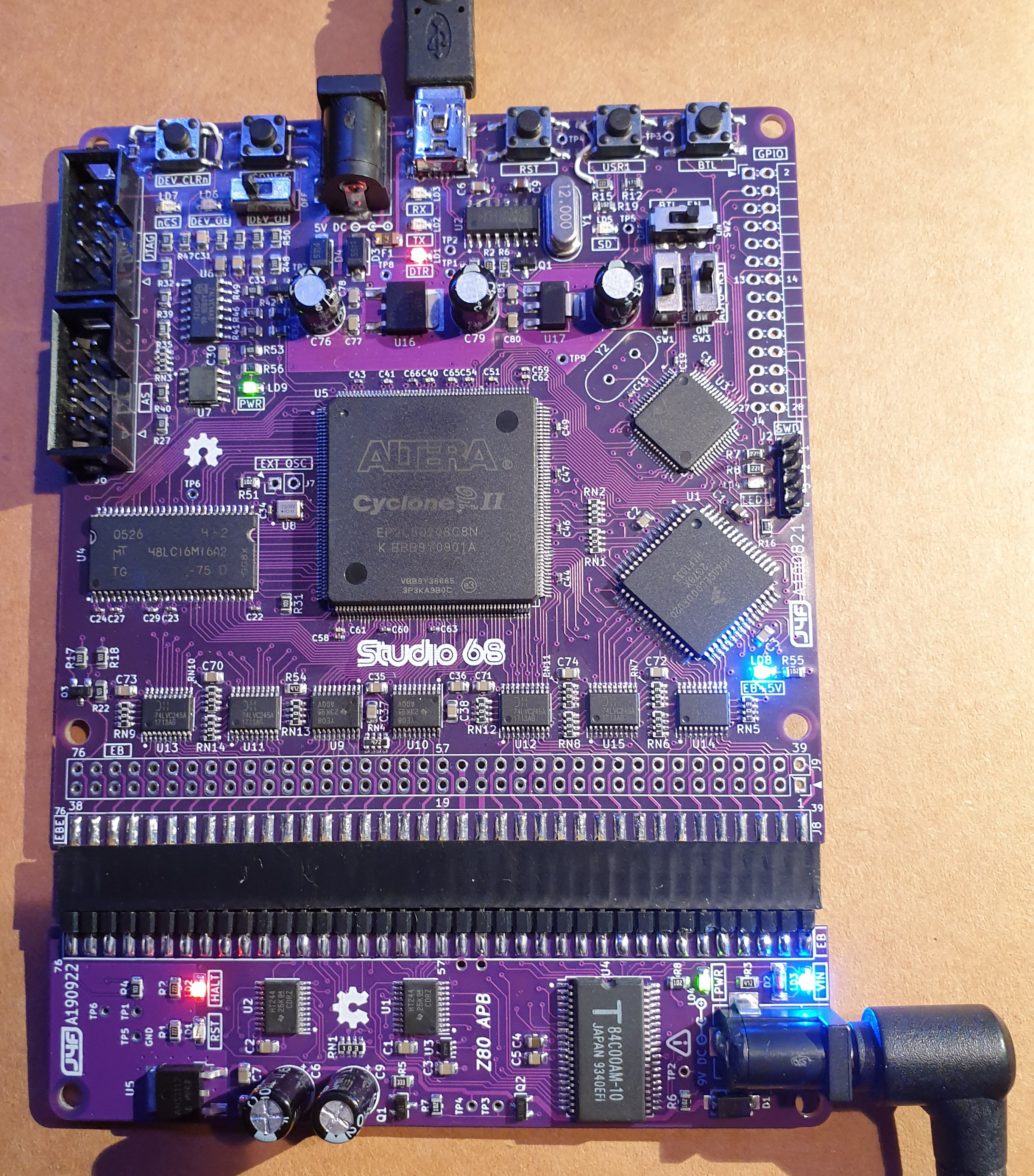
Here the Z80 APB + the Studio 68. The Studio 68 acts as "slave" with the 68SEC000 CPU held in reset to keep its data and address bus in high Z, exposing the RAM and I/O inside the FPGA on the external Z80 bus:
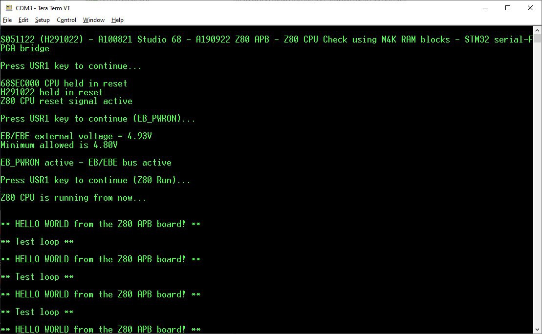
Here an "Hello world" test to check the I/O implementation inside the FPGA. Before enabling the external EB/EBE drivers, the STM32 checks if the voltage from the external power supply (in this case on the Z80 APB board) is "good". Then it enables the logic inside the FPGA and let the Z80 run:
* TBD *
* * Z80 BLINKING LEDS (BLL) BOARD * *
The Z80 Blinking Leds (BLL) board allows "to see" the status of the bus with some leds. Probably it isn't the most useful board but... I like blinking leds so I just did it...
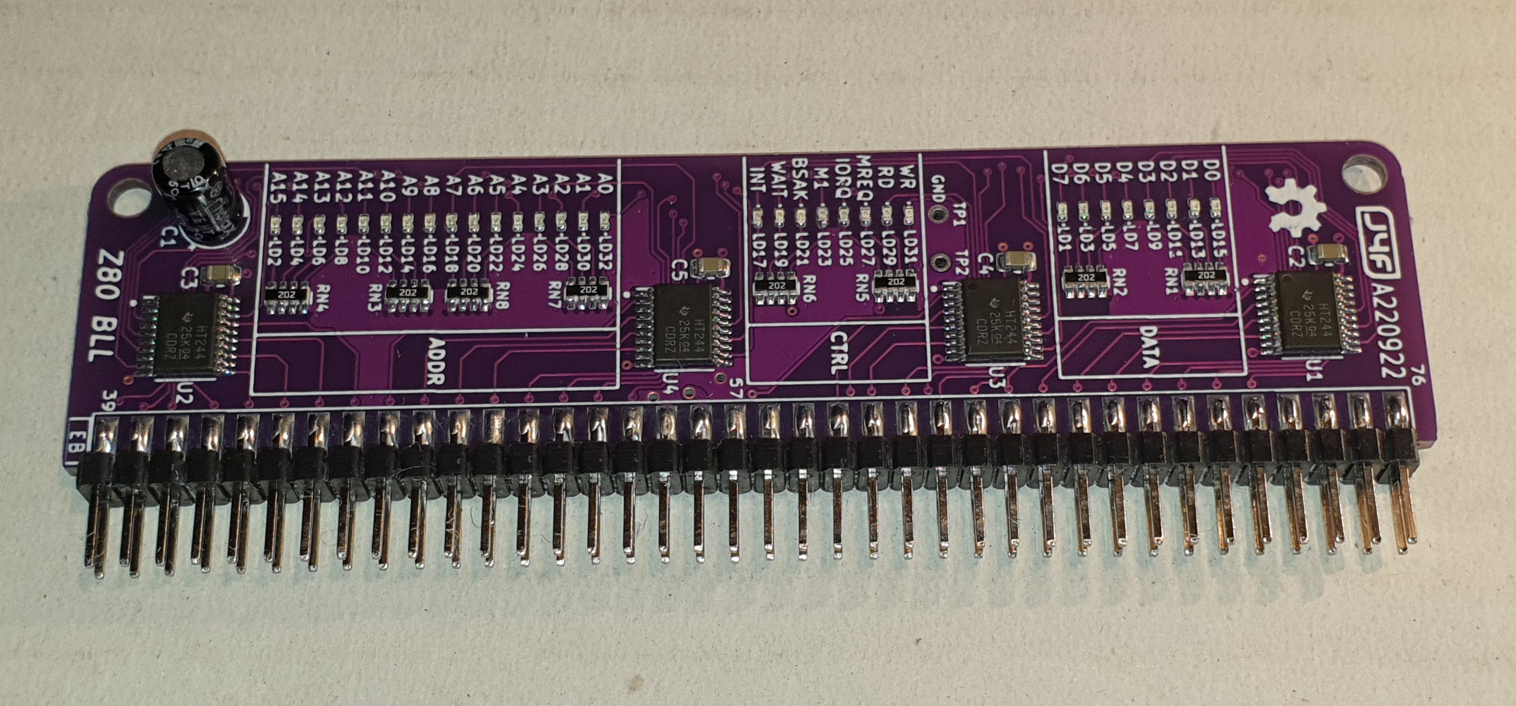
And here the result (in the photo the Z80 APB + the Z80 BLL + the Studio 68):
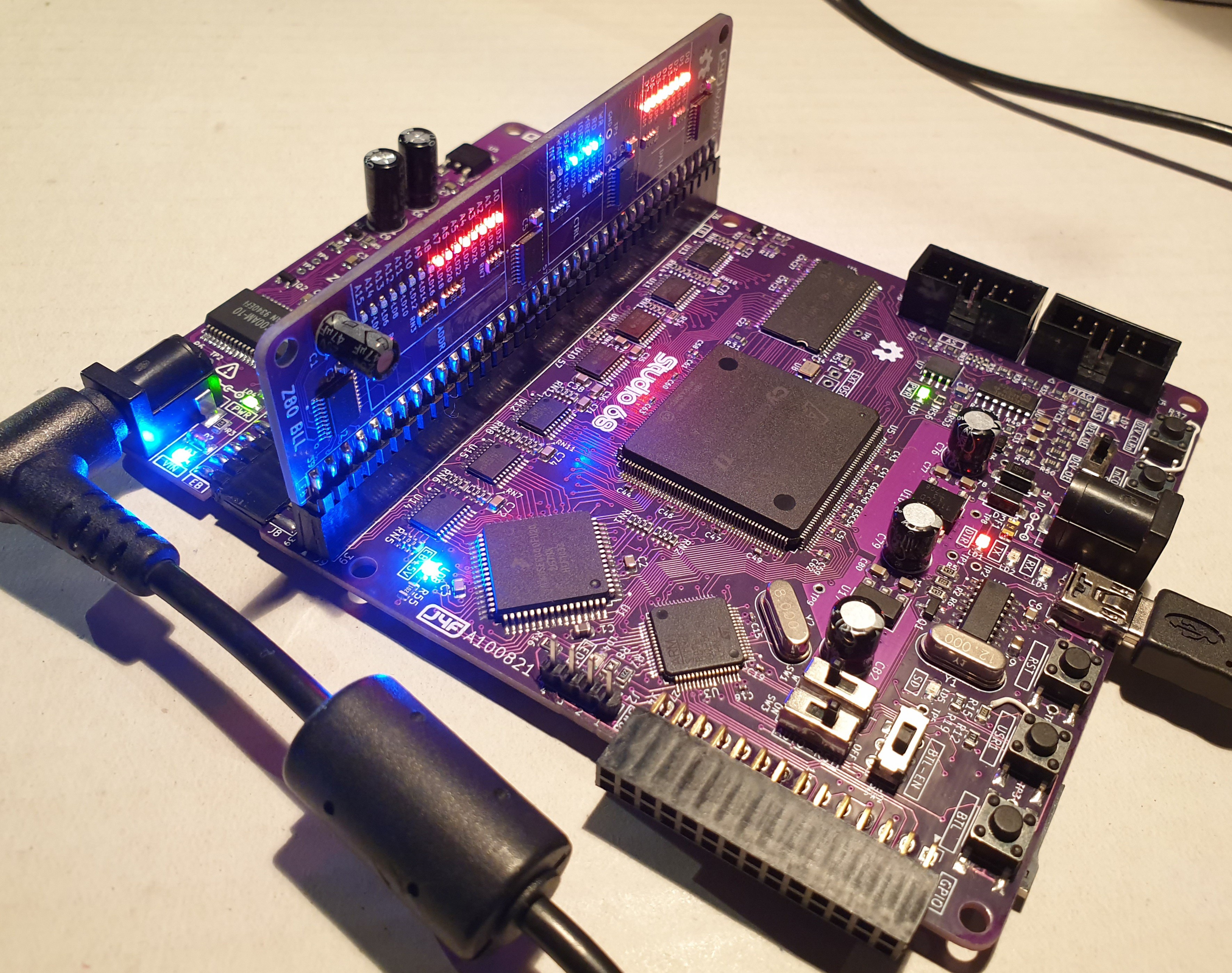
The power for the Z80 BLL board comes from the external EB/EBE bus, so it is drained from the power supply of the Z80 APB.
* * KR1801VM2 CPU APPLICATION BOARD * *
I've started testing a KR1801VM2 CPU (Soviet PDP11 "clone") with a custom "shield" for a custom development board I made previously (PicOne):
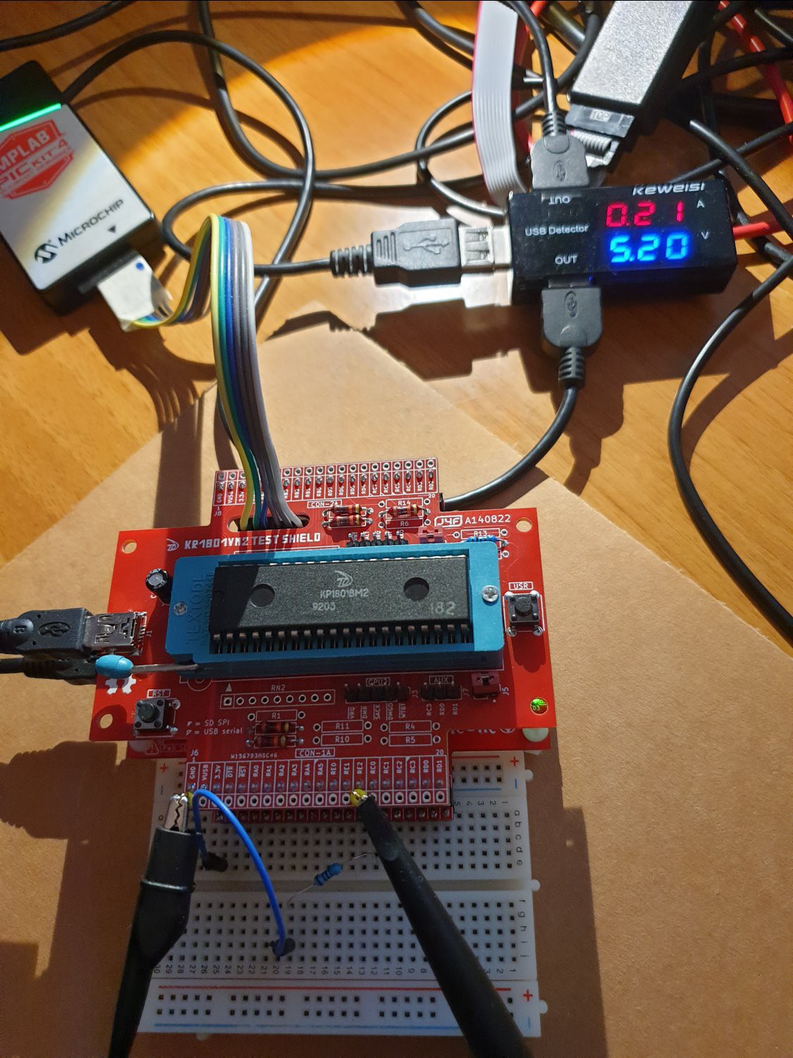
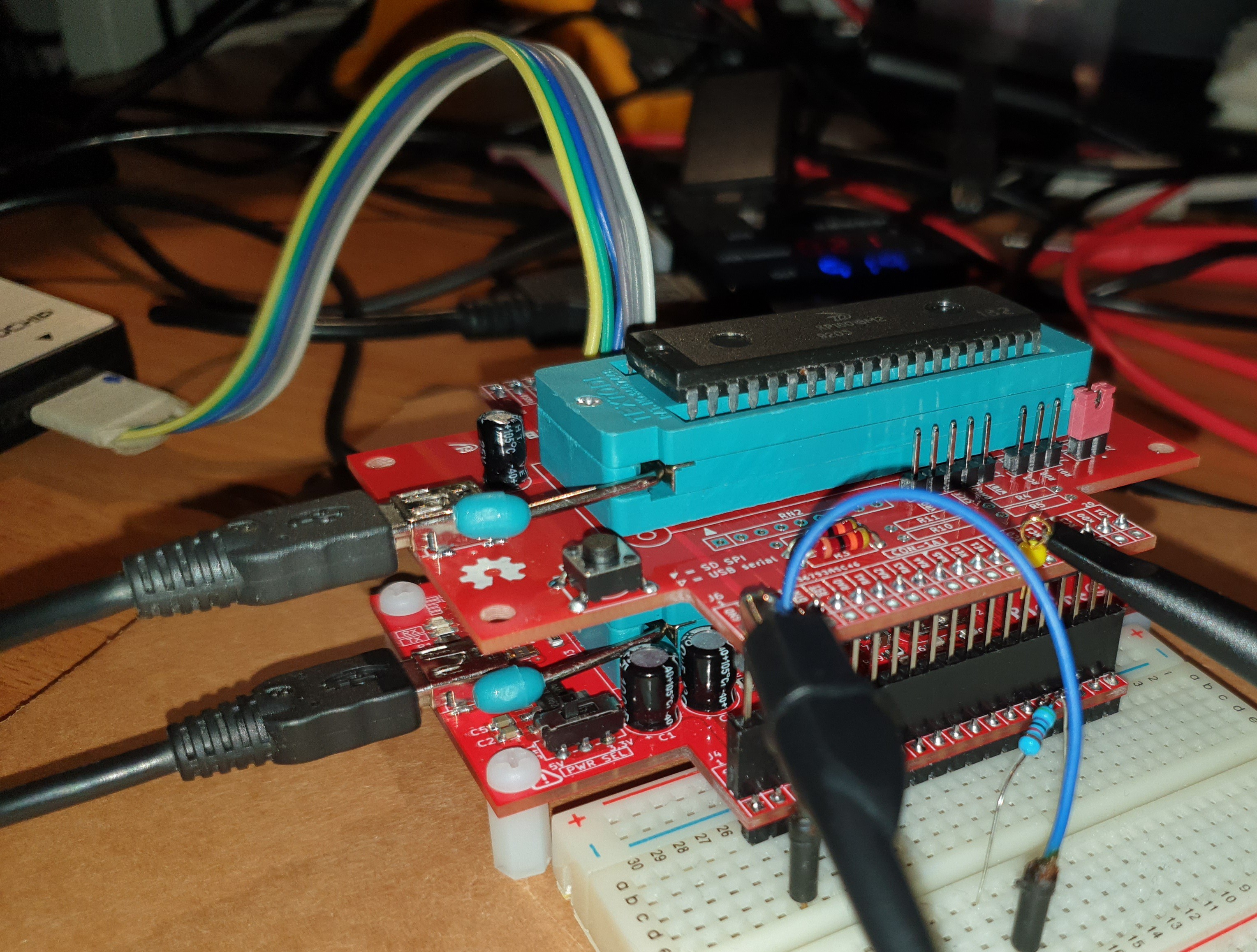
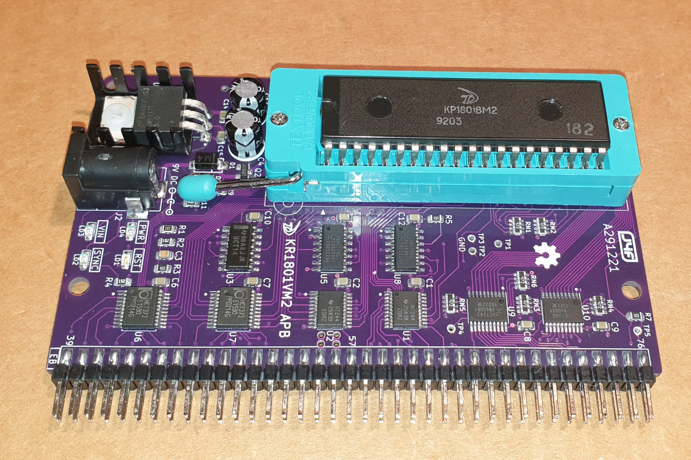
Here the the 4-layer PCB of the KR1801VM2 Application Board (APB). It should be possible to make with it something similar to a PDP11/03:
and here a first "hello world" test (KR1801VM2 APB + Studio 68):
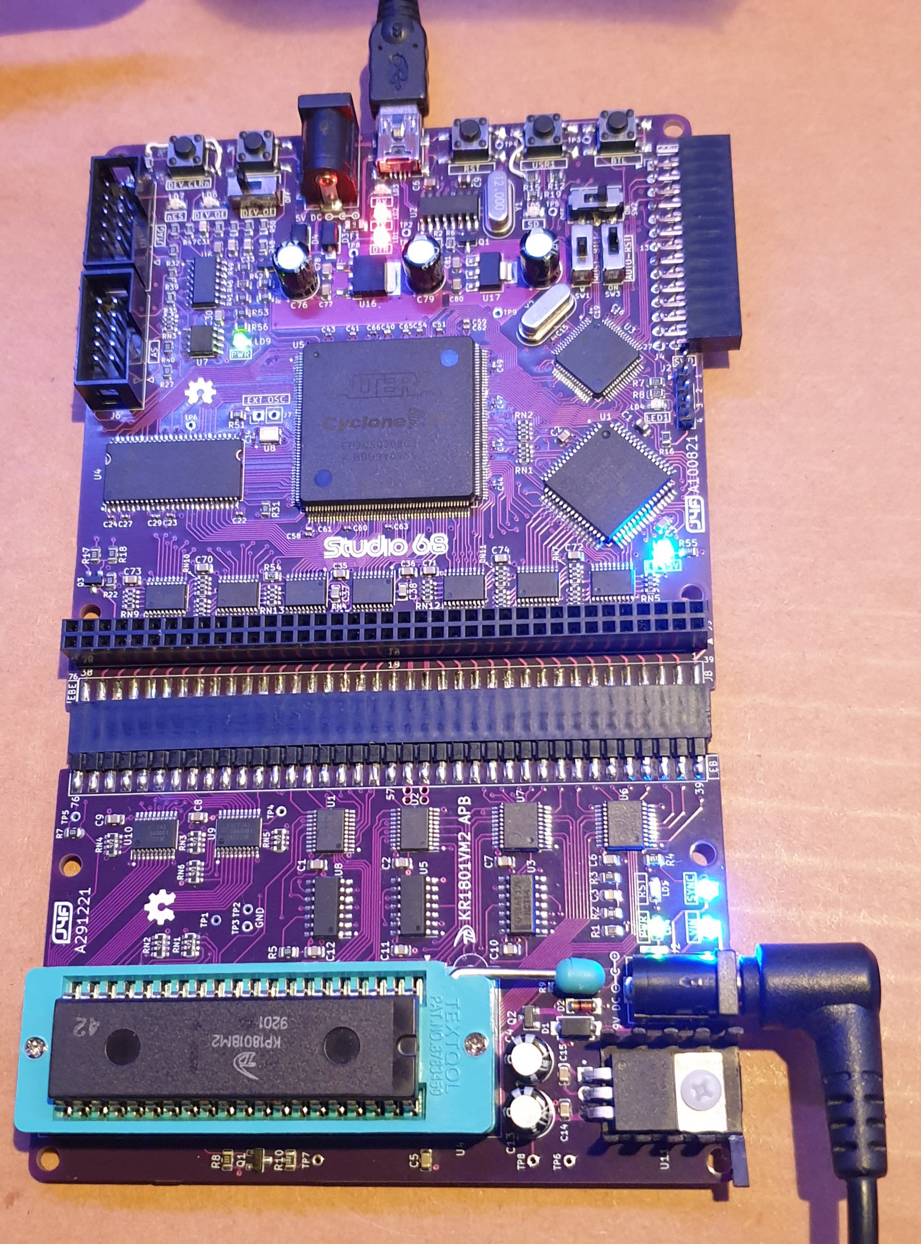

* TBD *
* * KR1801VM2 BLINKING LEDS (BLL) BOARD * *
Certainly could not miss a board with blinking leds, so I did the KR1801VM2 Blinking Leds (BLL).
The Z80 KR1801VM2 Blinking Leds (BLL) board allows "to see" the status of the bus with some leds. Bot the 16 bit Address...
Read more » Just4Fun
The studio industry continues to grow in today's time. People are making their future in this field. On this https://vinylio.nl/ post also you will be able to read about some such information. There is a link on the Vinyl LP when you go to their page. This will land you on a different webpage. On that webpage, you will get information about the multi niches. I have got to see a lot of new things by visiting this website.