 Christoph
I got this tip from someone else when I had to assemble my first 0201 board. It seems a bit weird at first glance, but it works very well!
The Idea
Your solder might come in paste form, but it doesn't have to be in that state when you place the components. You can pick up paste with a soldering iron and pre-tin pad by pad for all components you want to populate. No stencil involved, and you get immediate feedback and control over the applied amount of solder.
How it's done
- brush some flux gel on all pads you want to solder;
- place a blob of paste on a vacant spot on the PCB or on the frame. In most cases you have either one or the other;
- put a small tip on your iron - I use an angled pencil tip;
- set your iron to 220° C;
- repeat for all pads:
- with the iron, pick up some paste from the blob;
- then pre-tin a pad
- add more raw paste to the blob as required
The pads might look cold and bad after this, but we just need the right amount in the right places for now. Like so:
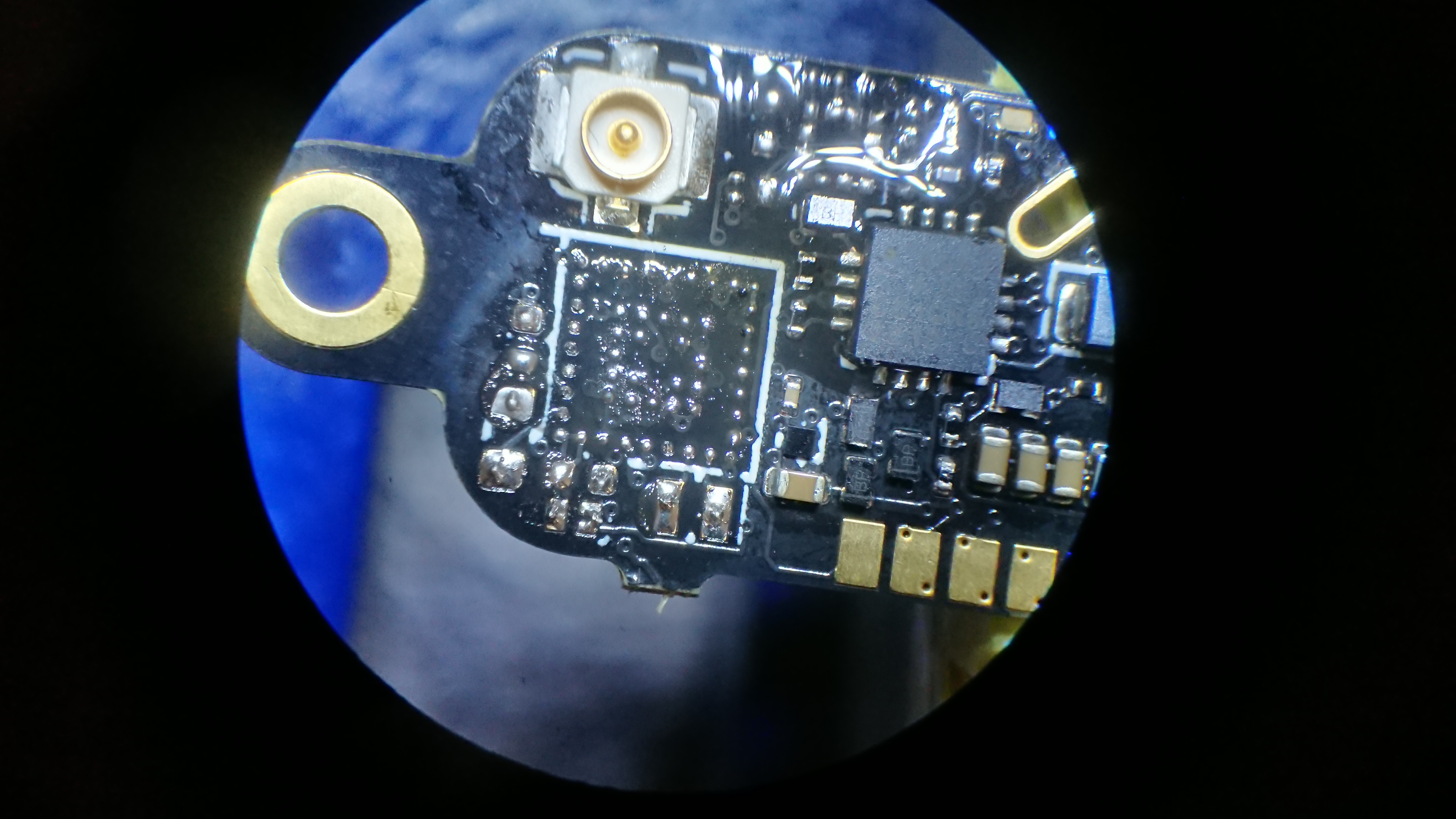
The footprint at the lower edge is for a FET in DFN1006B-3 (transistor package, about as large as the 0402 next to it), and the solder even bridges two pads (gate and source). All other pads look pretty much like inacceptable cold joints. That's not a problem though, because we'll level that all out with hot air:
- brush some flux gel on all pads you want to solder
- set hot air to 220° C
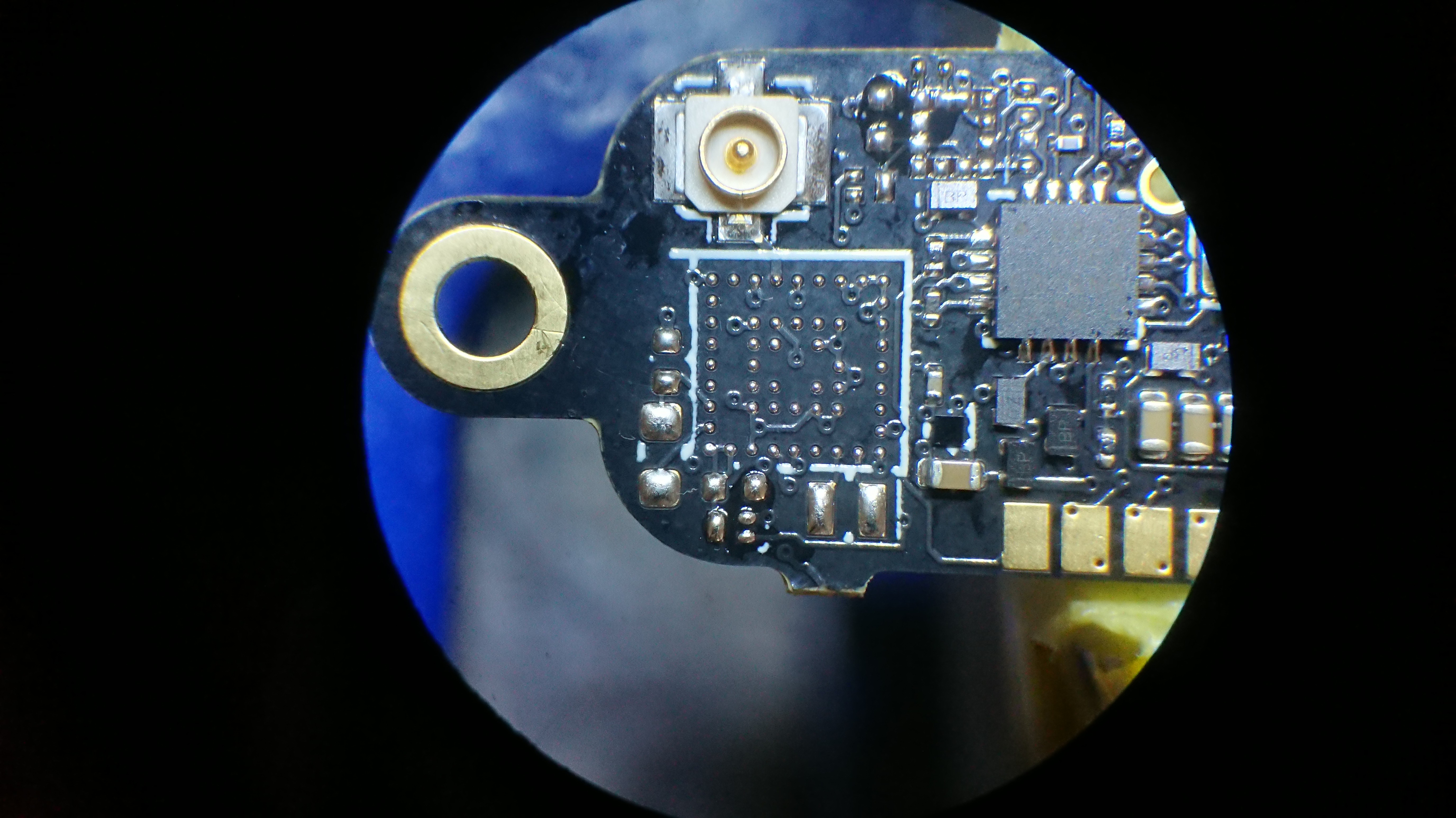
- level everything out
- touch-up with the iron where required (= if you have too little or too much solder on a pad):
- remove or add paste with the iron
- apply flux
- level out
- Clean the board
- brush on tacky flux gel
Now the board is ready for components:
This sounds very tedious, and somehow it is, but it's worth it and doesn't really take that long with some practice. Now place your components and reflow - the tacky flux will hold them in place:
Some more remarks:
- The solder pillows aren't first choice for 2-pin packages, because those tend to slide down the pillows. The solder will pull them into place during reflow anyway! If you want it super neat, apply paste manually for single chips and combine with the pre-tinning technique.
- Again, consider building in steps. If you would like to have a look at some solder joints from the side, don't place parts yet that would block the view.
- If you have massive ground planes in your PCB, consider heating it with hot air (say, to 120° C or something like that) and pre-tinning with an iron. That way it's much easier to get the solder to wet a pad.
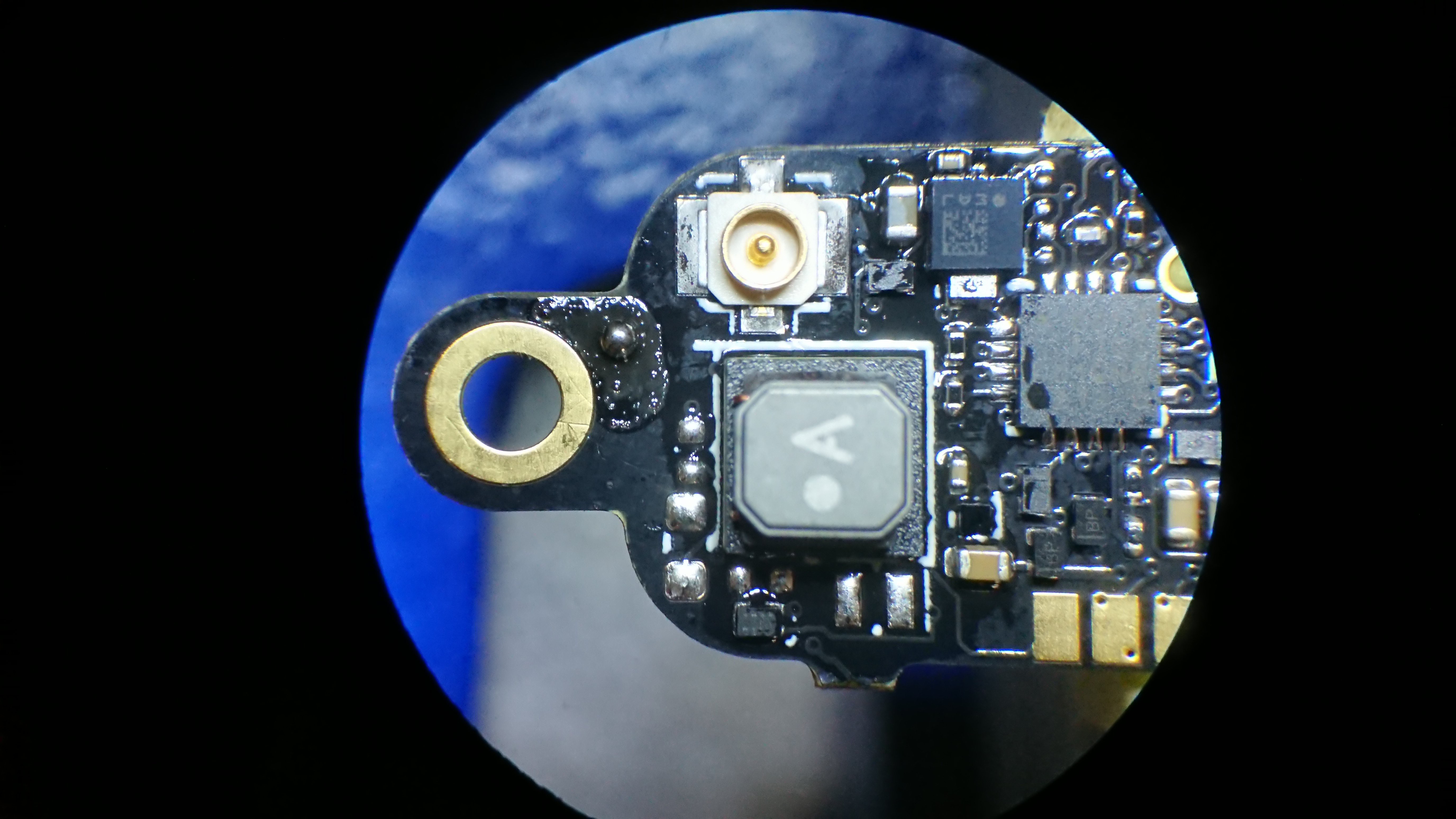
- Towards the top right is an LIS3MDL (has a QR code on it) with a diode just below it, and extremely close. I think we went a bit too far here because for some reason the diode was leaning against the LIS3MDL and slightly pushed it out of alignmnent.
- The large chip is a uBlox ZOE-M8Q in an LGA package, and so far it's been the nastiest I've ever had to solder. The pads are just 0.27 mm in diameter, and very hard to get tinned evenly and consistently. You really need a lot of patience and some practice for that thing - but still, it's in reach! This one also got a little 4018 inductor for extra weight on top, glued on with tacky flux. Just give it a bath in isopropyl alcohol afterwards and it will come off easily:
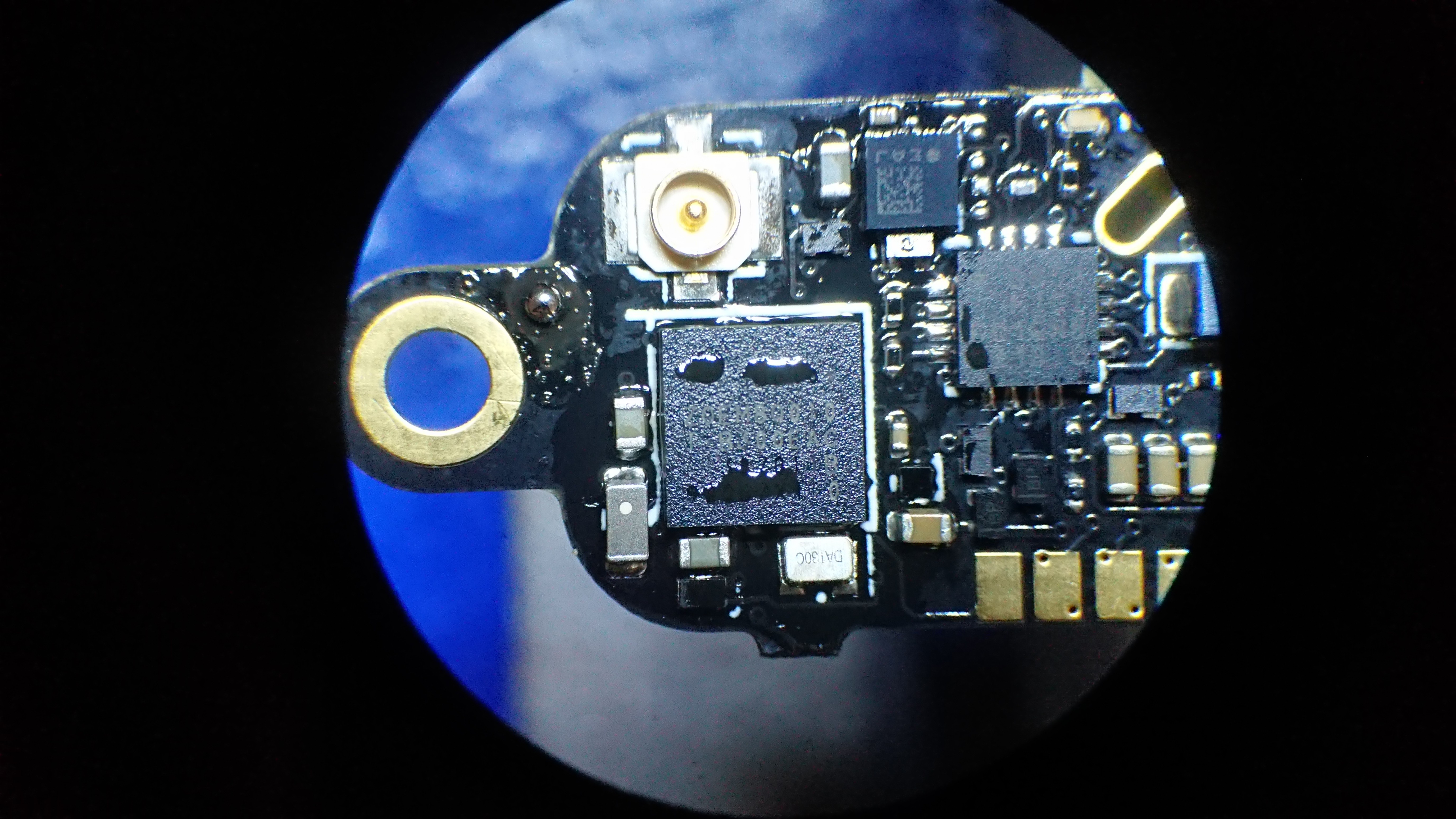
A little test with the multimeter in diode mode confirmed that at least the data lines (ZOE-M8Q's Rx and Tx, LIS3MDL's SCL and SDA) do have contact with the PCB. The rest I'll have to find out in some actual test runs.
Discussions
Become a Hackaday.io Member
Create an account to leave a comment. Already have an account? Log In.