BleakyTex
-
New booster, new microcontroller, decades of battery life
04/27/2024 at 16:20 • 0 commentsBooster v2.0
Even though the old booster is more efficient than those in most dosimeters on the market, it can be improved further. In fact, initially I chose the least elegant approach, just taking a conventional booster design and reducing its quiescent current through the use of low-power components and high-value resistors, but I made no architectural enhancements to it. The compact inductor I used wasn’t good for efficiency either. I was certain that there had to be a way to significantly lower the booster’s power consumption, yet I lacked any viable ideas.
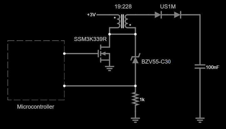
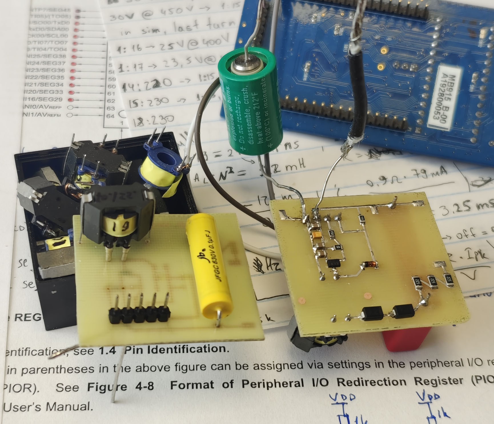
Later I realized that the correct solution was to take the feedback from the transformer’s primary winding — the same principle as in photoflash chargers like LT3484. The main benefit of that method is that it doesn’t waste energy on the feedback at all as there is no divider at the output to drain the capacitor. The 1:12 transformer enables the use of transistors rated for lower voltages, as they have better characteristics than the high-voltage ones. Two ultrafast 1000V diodes and a 100nF 630V polypropylene film capacitor are used to minimize the HV leakage.
I also decided to use a different battery because LR44 batteries cannot deliver enough current for the new booster to work efficiently. Furthermore, with a larger battery and the more efficient booster there’s an opportunity to prolong the dosimeter’s single-charge lifespan for more (maybe a whole lot more, see below) than half a dozen years, eliminating the need for battery replacement entirely. I really wanted to use a battery with low self-discharge but they turned out to be unsuitable: Li-SOCl₂ batteries are dangerous and produce too much voltage to safely drive the LCD, Li-CFx batteries have too high ESR which increases even more at low temperatures. I went with a CR1/2AA 950 mAh Li-MnO₂ battery, as it can easily deliver sufficient current to the booster at a price of having higher self-discharge than the other two options, but not by much. With all those improvements the new booster consumes 0.56 µA at a normal background radiation level, quite a step up from 8.6 µA in the prior design.
![]()
The new booster [simulate the circuit]
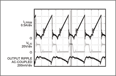
In retrospect, the solution to the problem of designing an efficient booster was right in front of me from the very beginning. While doing initial research I saw many articles mentioning the voltage waveform on the inductor; it’s a short pulse (VLXI) that begins when the transistor is closed, its amplitude equal to the output voltage if a regular inductor is used. If a transformer or an autotransformer is used, the pulse amplitude is divided by the transformer turns ratio (1:12 in our case).![]()
Switching waveform in a boost converter [source]
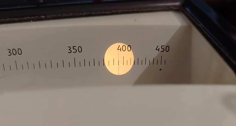
The idea is to keep switching the transistor until the VLXI (kickback pulse of the primary) reaches roughly 400V / 12 = 33.3V. A 30V Zener is used to signal the microcontroller to turn off the booster when the VLXI had reached the desired voltage. I'm not sure why a 30V and not 33V Zener works, something is probably suppressing the peak of the kickback pulse but with a 30V Zener the booster stops when the output reaches 405V.What’s left is to estimate when the dropping voltage in the output capacitor reaches a threshold value and then schedule a booster restart at the predicted moment. With this approach the output voltage is bound to fluctuate quite significantly because there is no way of knowing when exactly to recharge the capacitor since the voltage at the output cannot be measured without turning the booster on. Thankfully there is no need to keep the Geiger tube voltage at exactly 400V, since its minimum operating voltage is 380V, so just keeping it above 380V should be good enough.
Transformer design
The rest of the circuit revolves around the transformer, so it’s gonna be the main focus of this post. I decided to use the RM5/I 3C90 gapless ferrite core because it’s the largest core that fits in the pen form-factor while having enough inductance per turn; high inductance is required since the microcontroller cannot switch the transistor on for less than 30.5 µS because it’s clocked by a 32.768 kHz crystal to keep the power consumption low.
The high-voltage transformer should be designed in a way that keeps the sum of all losses at a minimum. That includes:
- Resistive loss in the battery due to its ESR plus loss of its capacitance due to high current draw. This puts a limit on how high the primary current can be, effectively imposing a lower limit on its turn count. Also too few turns in primary will cause a core saturation as the primary with a small number of turns will have low inductance and thus the current through it will rise faster, and there’s a lower limit on the transistor on time as described above.
- Loss in the transistor.
High-voltage transistors have high RDS, Cout, and VGS(th), this puts a lower limit on the turns ratio as transistors rated for lower voltage have better characteristics — the lower the voltage the better. However, if the turns ratio is too high, the losses in secondary will increase. - Loss in the secondary.
The more turns the secondary has (high turn count in secondary means high turn ratio), the higher its parasitic capacitance, Cpar: in each operating cycle, the more Cpar × V²out / 2 of energy gets lost due to it, so less cycles means lower loss. This in turn sets an upper limit on the primary turns count which is inversely proportional to the current in primary, and thus the energy transferred per cycle.
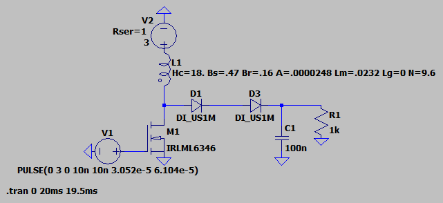
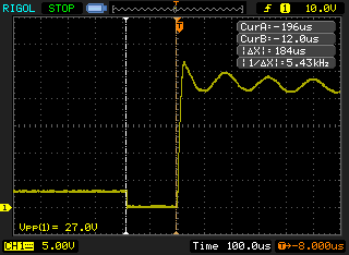
The primary shouldn't saturateInitially I just wound a 10:150 transformer, expecting primary’s inductance to be 200 µH and thus a 450 mA peak current at 16.384 kHz 50% duty drive. The saturation current was calculated here and I got 580 mA, so I wasn’t expecting the saturation to happen. I was using a 30V IRLML6346 transistor and a 1000 µF bypass capacitor to provide the energy for the transformer. The idea was to have lower primary inductance and thus higher current to transfer as much energy per cycle as possible to minimize the CV² / 2 losses in the FET and secondary winding. The less cycles it takes to get from 0V to 400V, the lower the capacitive losses will be. Didn’t work all that well… When I powered the boost converter from the battery, it warmed up a bit. I measured the current in primary winding and saw this:
![]()
High current through the primary due to core saturation, 1 mV/mA
My tinyCurrent (clone of the uCurrent) couldn’t even show the whole picture as the inductor current was way above 1.5 A. Simple formulas for saturation don’t always work, apparently. After some time in Google I found out that LTspice is capable of simulating the non-linear behavior in inductors by using the Chan model, which is both accurate and easy to use. We need the following parameters for the simulation:- Number of turns (N)
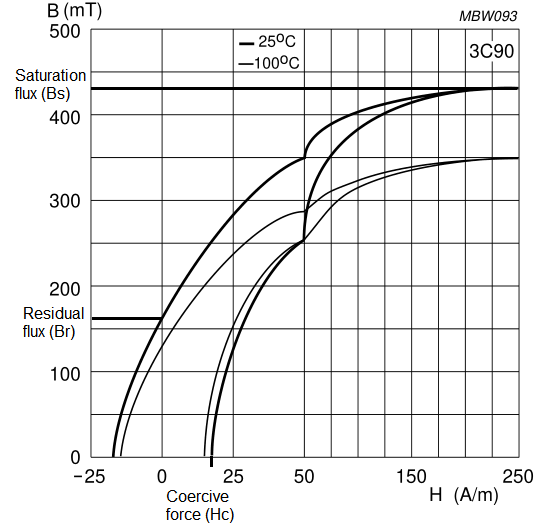
From the 3C90 material datasheet (magnetic properties):
- Coercive force (Hc), in Amp-turns/meter
- Residual flux density (Br), in Tesla
- Saturation flux density (Bs), in Tesla (must be taken from the table, not from B-H curve)
From the RM5/I core datasheet (geometric parameters):
- Magnetic length (Lm), in meters
- Length of the gap (Lg), in meters
- Cross-sectional area (A), in square meters
![]()
B-H curve from 3C90 datasheet
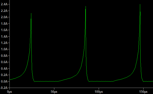
The coercive force Hc is the value of H when B = 0 at the bottom of the graph. The residual flux Br is the value of B when H = 0 at the left. The rest of the values are stated in the datasheet for the ferrite.Here’s the LTspice simulation I used. Unfortunately, it cannot simulate transformers (coupled inductors) with this kind of model, so I’m just simulating the primary winding here. The number of turns is 9.6 instead of 10 because the last turn is not a full turn as the wire has to be routed to the bobbin’s pin halfway in.
![]()
![]()
I (L1)
Looks pretty close to what I got in practice. After some poking around I found out that 19 turns in primary creates the best balance between the peak current, the transistor voltage, and the number of secondary turns. The final version of the transformer has 19 turns in primary and 228 turns in secondary. I went with a 1:12 turns ratio because it allows me to use a FET with low enough voltage rating, without needing too many turns in secondary at the same time. At 400V output and 3V supply such a transformer will produce a 3 + (400 / 12) = 36V kickback pulse. The transistor should be able to withstand this voltage. Transistors rated for higher than 45V have suboptimal RDS, output capacitance, and gate threshold for the task. I’m using an SSM3K339R FET, it’s rated for 40V.Let’s simulate this transformer coupled with the new transistor and check how well the simulation fits the experimental results.
![]()
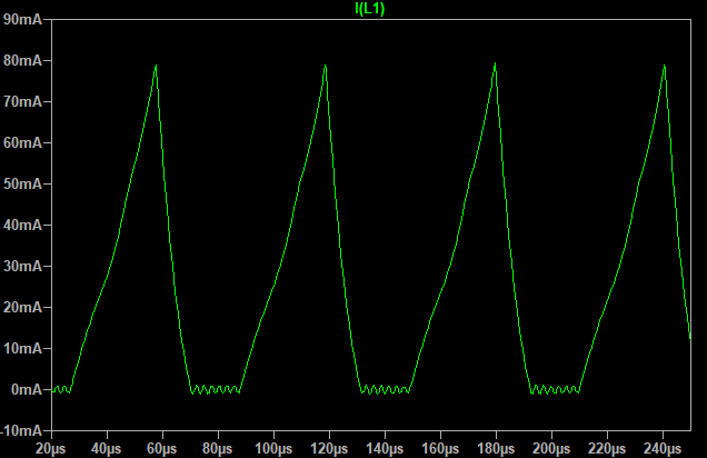
Simulated primary current ![]()
Primary current (blue, 1 mV/mA) and battery voltage (yellow) in the real booster
Would you look at that, the peak current is 78.9 mA in simulation and 78.4 mA in practice. The average current is 18.2 mA which is optimal for the Li-MnO₂ battery; it shouldn’t lose its capacity due to high current draw.Discharge time matters too
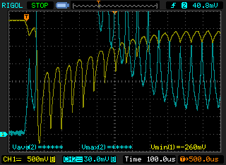
While on the oscillogram above the inductor current has a rather nice waveform, it’s not always like that. With the 16.384 kHz 50% duty drive, when the boost converter begins the charging cycle and the voltage in the output capacitor is near zero, the transformer won’t have enough time to transfer all of its stored energy into the capacitor, and that in turn will increase the current in primary, overloading the battery:
![]()
Overcurrent in primary (blue, 1 mV/mA) and the corresponding battery voltage drop (yellow)
Note: the current doesn’t drop to zero anymore because I connected four 10uF 16V X5R capacitors in parallel with the battery to reduce its peak load. This reduces the resistive loss due to the battery’s ESR, and also prolongs the battery life since high loads reduce battery’s effective capacity. Such capacitor configuration is used to achieve lower leakage through them, which was 5 nA in my case. There’s a good appnote from SiLabs on this topic.It’s easy to show that the transformer discharge time depends on the voltage at the output capacitor by deriving the time from the well-known formula for the charging inductor current:
The discharge inductance in case of an autotransformer is the sum of inductances in primary and secondary:
Ldis = 122 mH
Same for the winding resistance, which is a sum of resistances in primary and secondary:
Rdis = 26.3 Ω
Ipk = 78.4 mA, as measured on the oscillogram above.
The initial voltage in the output capacitor equals the 3V supply. Plugging the numbers in shows that the transformer takes 5.5 ms to fully discharge when Vout is 3V, but when it gets to 50V the discharge time shall drop to 0.2 ms.
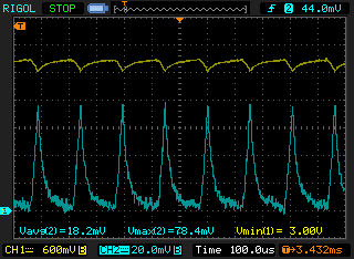
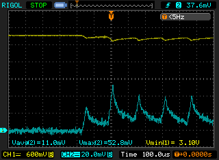
I didn't do the numbers when I was experimenting, I just intuitively set the PWM output to 6.5 kHz, 20% duty (30 µs charge time, 0.12 ms discharge time) and this almost eliminated the current spike:
![]()
Current spike in primary (blue, 1 mV/mA) is almost gone, battery voltage (yellow) doesn’t drop to zero anymore
The battery easily handles a single 52.8 mA pulse, never dropping from its resting voltage in full. There’s still some room for improvement but that’s a story for another time.As for the booster restart delay estimation, I’m not sure yet on the exact algorithm. The measurements tell that, even though the tube consumption is easy to measure by just counting its pulses, the capacitor leakage is bound to fluctuate depending on the environmental conditions such as temperature and humidity, so the algorithm will have to estimate that leakage on each recharge cycle.
Winding technique for the lowest losses
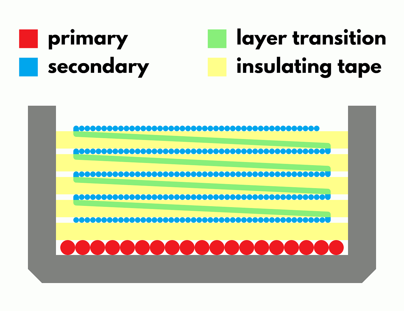
The parasitic capacitance in the secondary winding causes significant losses, so the transformer must be wound in such a way that reduces it. I’m using two methods described here (explained in more detail here).
![]()
Cross-section of a transformer bobbin
Each winding layer has to be separated from its adjacent layers with insulating tape to increase the distance between them, this is the first measure to reduce the stray capacitance. The primary (0.224 mm wire, 19 turns) is wound in one layer at the bottom of the bobbin, the secondary (0.07 mm wire, 228 turns) is wound in 4 layers of 46 turns, last one is 44 turns. All layers of wire start at the same edge of the bobbin. When layers are wound starting from edges opposite to one another the capacitance is at its highest: if the first turn of the previous layer is opposite to the last turn of the next, there’s twice the voltage per layer between those turns. As the energy stored in the self-capacitance is proportional to voltage squared, this more than offsets the lower voltage difference at the other side of the winding. Lower capacitance can be achieved by winding each layer in the same direction, with a section of wire in between layers to return to the other edge, so the wire is wound right to left, then right to left again on the next layer, see the photo below. That way the voltage between layers becomes uniform.All those measures described above increase the conversion efficiency by 17%, resulting in a total efficiency of 65% at 3V input and 400V output, which is comparable to the commercial solutions.
![]()
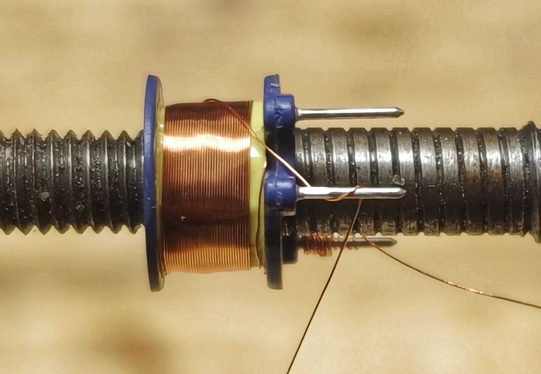
The transformer being wound ![]()
Two booster prototypes
Revisiting the tube consumptionIn the first log I estimated the tube consumption using a rule-of-thumb formula, but never got to test the numbers in practice. But first let's check how much energy is being lost in the booster’s capacitor and the output diodes.
I connected an electrostatic voltmeter with >1011 Ω input resistance to the HV capacitor and started the booster that charged the capacitor to 400V and turned off. The voltage has dropped by 7V in 10 minutes, which is 0.0117 V/s; linear approximation is fine at such a small voltage drop.
Since the current is the amount of charge transferred per unit time, the leakage current can be calculated using the formula for the charge stored in a capacitor:
Then the battery consumption due to the HV leakage is:
While the booster’s efficiency in charging the capacitor from 0V to 400V is 65%, it drops to 53% when recharging the capacitor from 380V to 400V, so I used 53%.
Got the estimate for the leakage, now let’s see how much current the tube is consuming. I charged the capacitor to 400V and connected an M4011 tube to it. I decided to ditch the SBM-20 because M4011’s intrinsic noise is 5 times lower compared to SBM-20 and the sensitivity is pretty much the same. Then I placed a radioactive source near the tube and the voltage dropped by 10V in 11 seconds, so the impact of leakage (0.0117 V/s) on the measurement is negligible. The tube has produced 299 pulses over that period.
The total charge the capacitor lost is as follows:
So, a single pulse consumes:
The rule-of-thumb formula gives 1.6-ish nC. Good enough for me, at least it’s correct within an order of magnitude.
Given that the tube has 400V applied to its anode and, under normal background radiation, produces 0.33 pulses per second consuming 3.3 nC per pulse, its power consumption is:
Given the 3V supply voltage, the tube's battery consumption is:
The total consumption of the booster, driving the M4011 tube exposed to normal background radiation is 550 nA. Looks good so far, though I want to try and reduce the leakage even more. VS-E7MH0112-M3 diodes, for example, should leak even less than US1M’s.
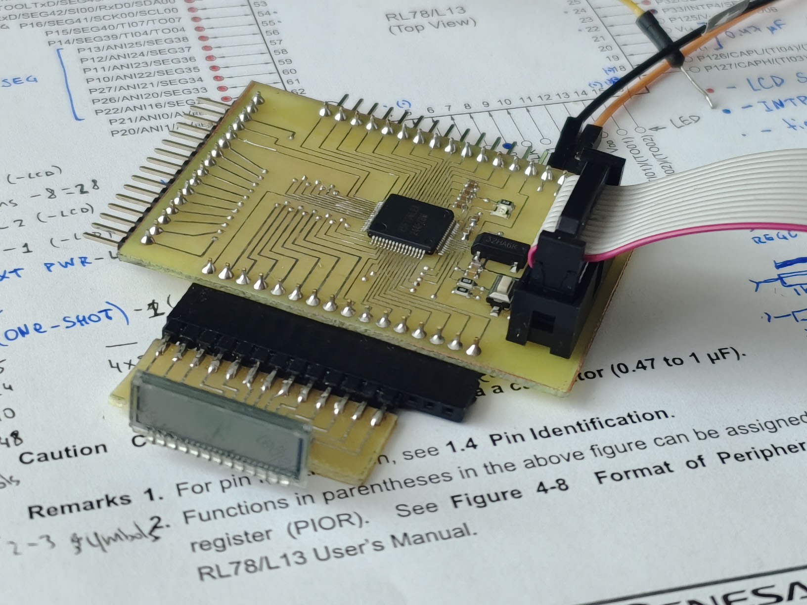
A new microcontroller
Long after I made the first revision of this Geiger counter, I noticed that the entire STM8 product line was going to be discontinued (late update: not anymore, but the damage has already been done). That, combined with the new booster design requiring neither a comparator nor a voltage reference, made me reconsider my choice of the microcontroller. And I did find a much better one. Behold, the RL78/L13 series from Renesas. There is also the L12 series which consumes slightly less but it also has less flash memory capacity, and I want a lot of it for the measurement logs. I got an R5F10WLEA and made a breakout board for it to see what it’s capable of:
![]()
R5F10WLEA breakout board
Since the microcontroller is going to spend most of the time in sleep mode, with just the RTC and the LCD controller running, consumption while sleeping matters the most and, according to my measurements, the RL78 chip only draws 0.5 µA. The STM8L was drawing 2.4 µA in the same mode. Also there’s no need to run the code from RAM this time, since RL78 is consuming 4.1 µA while executing from flash; STM8L consumes 5.5 µA executing from RAM with flash disabled. Since the core is active for less than 0.75% of the time (<15 ms every 2 seconds), it contributes less than 31 nA to the total consumption.The microcontroller consumes 0.53 µA, the booster consumes 0.55 µA, the battery self discharge current is 1 µA (1% of capacitance per year), so the total power draw is 2.1 µA. Considering that the circuit can utilize up to 90% of the battery, the effective capacitance of a 950-mAh Li-MnO₂ battery is 855 mAh. With 2.1 µA consumption from a 855-mAh battery the device can, in theory, last for 46 years. Impressive, huh?
Of course it won’t last that long in the real world, although at this point the main limiting factor is not even the device itself but the self-discharge of the battery, and it can vary a lot. I need more experiments to confirm that those numbers are true, but even if they’re worse by a decimal order of magnitude, which they most likely aren’t, the new dosimeter design is going to last multiple years from a single CR1/2AA cell.
-
Firmware update and future plans
03/20/2023 at 16:54 • 0 commentsI am finally able to post the firmware, it has been rewritten in full assembly by @hidefromkgb and executes from RAM. As I expected, the device now consumes around 17-18 uA which means around 11 months of battery life, maybe even 12, since the previous firmware version lasted for 5 months instead of expected 4 months. However, I'm starting to have bigger plans for it. I realized that there is a lot of unused flash memory that can be used to log radioactivity data and display it via PC interface. Also check the drawing of a custom LCD that the final version may get:
![]()
There also will be a major update to the HV booster to get as much efficiency as possible with this form factor but it requires a custom transformer, and it will take some time to design and make. Two years of battery life is the new goal!
-
A small update
01/27/2023 at 19:18 • 0 commentsIt's been 4 months and this thing is still running fine. The battery voltage is 2.2V, so I'm expecting it to run for another month or two. Also the code has been rewritten in assembly and now executes from RAM, though it still needs some polishing, I'll post the details in the next update. Disabling flash reduced the consumption by 25 uA and now the entire device consumes 19 uA, which means 11 months of battery life. I've also managed to find some better parts which should reduce the PCB size and power consumption even further. My current goal is 1 year of non-stop operation.
-
First prototype
10/11/2022 at 18:22 • 0 commentsIt's working!
There are only two things left to implement — LCD display functions and basic control functionality: sound switch, backlight, buttons for switching display mode and resetting the dose. I don't see much point in explaining how it works, let's get to the results instead. The total current consumption when counter is idling is 44 µA, which is low enough to avoid the battery capacitance derating. Given that the speaker is disabled, and battery capacitance is 150 mAh (the device stops working at 1.8V, so we can have individual cells discharged to 0.9V, utilizing their full capacity), this gives us a total working time of 3409 hours or 142 days or 4.7 months. This is a best-case number, so I've rounded it up to 4 months. I've left the device turned-on and will post the actual number of days it managed to last. At the moment of writing this, it has been working for 12 days non-stop without any problem and the battery loses around 8mV per day.
I'm happy with the code performance too. The whole update routine (radiation rate, dose calculations, time update and LCD print function) takes only 16 ms or 524 clock cycles. We save some power because the CPU spends so little time in the active mode. A friend of mine decided to rewrite the firmware in full assembly, optimizing it even further. I will post an update if he will actually do it.
Here's some photos and a video of a finished device. It was designed with an enclosure in mind but apparently, I won't be able to make it any time soon.
![]()
![]()
Source code and schematics are available on my Github.
-
Data processing
10/09/2022 at 00:24 • 0 commentsSetting the update interval
To save power, I've decided to update the display once in 5 seconds. Dose rate is a statistical value, so there's not much point to update it faster. Between updates we can stop the CPU, since the boost converter and the radiation event counter work independently of it. We have one last timer to spare, and we're going to use it to generate CPU wakeup interrupts every 5 seconds. After wakeup, we'll update the dose rate and total dose values and put the CPU back to sleep until the next interrupt. First, we should set up the timer:
  /* TIM4 SETUP (5-SEC INTERRUPTS) */
  CLK_PCKENR1_bit.PCKEN12 = 1; // Enable TIM4 clock
  TIM4_PSCR_bit.PSC = 0xE;     // Div by 16384 -> 0.5 sec resolution
  TIM4_ARR = 9;                // 5-second period (sec =  + 1) / 2)
  TIM4_EGR_bit.UG = 1;         // Update timer registers to apply prescaler value
  TIM4_CR1_bit.CEN = 1;        // Start the timer

  TIM4_IER_bit.UIE = 1;        // Enable TIM4_UIF interrupt (timer overflow)
  WFE_CR3_bit.TIM4_EV  = 1;    // TIM4 interrupts can wake the CPU from Wait mode
And then we just call the update function when the CPU is woken up by interrupt from TIM4 and then put it back into Wait mode after the function is executed:
int main(void)
{
...
  FLASH_CR1_bit.WAITM = 1;   // Disable Flash memory during Wait mode

  while(1)
  {
    if (TIM4_SR1_bit.UIF == 1) {
      TIM4_SR1_bit.UIF = 0;  // Reset interrupt flag
      app_readGeiger();
    }

    asm("WFE");  // Enter Wait mode
  }
}
Notice that this happens in the main loop, there is no interrupt handler. Since there's nothing time-critical happening here, we don't need them, we'll just waste precious CPU cycles to enter and exit an interrupt.
Reading the event counter and applying dead-time correction
The challenge with reading the value from the timer is that the event may occur during reading process, causing rollover or missed readings. Also, we should apply dead-time correction to the value we've read because at high counting rates, a Geiger tube may not have enough time to recover to register pulses occurring at quick succession, which leads to reduced measured activity. The equation for the dead-time correction is:
where N — true counting rate (in events per second), n — measured counting rate, Td — dead time of the tube. This equation is meant for 1-sec measurement intervals, and we're measuring with 5-sec intervals. This will reduce the dead-time effect by 5. The dead time of SBM-20 tube is 190µS, so the effective dead time will be 190/5 = 38µS:
This equation involves floating-point numbers and will be too challenging to calculate for an 8-bit microcontroller, running at 32.768 kHz. We can simplify it with a polynomial approximation:
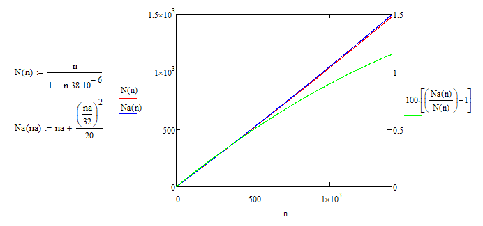
Now we can calculate N only using integer numbers. Before we get to coding, let's see how accurate our approximation is. For this, I'll plot the original equation and its approximation for n = 0 to 1400 CPS, which is the maximum counting rate for SBM-20.
![]()
Red line — original equation, Blue line — approximation, Green line — deviation in % The deviation increases with n, and at 1400 CPS the approximation gives a value, that's 1.15% higher than the original equation gives. Not too much accuracy to lose, given a massive performance gain that we get from this approximation, isn't it? Let's write the code. Since we need to read and clear the timer as fast as possible, I'll use assembly to do this. And while I'm at it, I'll do the dead time correction in assembly as well. You can check the STM8 programming reference (PM0044) if something isn't clear.
uint16_t cp5s;                 // Registered events during 5-sec interval

void app_readGeiger(void)
{
  // Read and clear TIM3 counter
  // TIM3_CNTRH must be read first to prevent rollover
  asm("LD   A, TIM3_CNTRH");
  asm("CLR  TIM3_CNTRH");
  asm("PUSH TIM3_CNTRL");
  asm("CLR  TIM3_CNTRL");
  asm("PUSH A");
  asm("LDW  X, (0x01, SP)"); // now both stack and register X hold cp5s value

  // Apply dead time correction: cp5s = cp5s + ((cp5s/32)^2 / 20)
  // This equation is a polynomial approximation of N = n / (1 - n*38e-6)
  asm("LD   A, #32");
  asm("DIV  X, A");   // cp5s/32
  asm("LD   A, XL");
  asm("MUL  X, A");   // ^2
  asm("LD   A, #20");
  asm("DIV  X, A");   // /20
  asm("ADDW X, (0x01, SP)"); // + cp5s
  asm("POPW Y");
  asm("LDW  cp5s, X"); // cp5s =
}
Only 15 instructions, not too bad. The rollover is prevented by using the fact that the MCU locks the timer counter value if we first read the TIM3_CNTRH register and unlocks it after TIM3_CNTRL is read. Thus, our timer ignores radiation events for only 4 instructions (CPU cycles) every 5 seconds.
Calculating radiation dose rate
Dose rate is a statistical value, and a 5-sec interval is not enough to get a reasonably accurate measurement. A reasonable trade-off between accuracy and response time is a 1-min measurement. But how to update the display every 5 seconds if our measurement interval is 1 minute? One way to calculate counts-per-minute (CPM) is from a rolling sum of 12 consecutive 5-sec measurements. Every 5 seconds a new measurement is added to the sum and 12th last is subtracted from it. Algorithmically it looks like this:
cpm -= event_buf[event_idx];
cpm += cp5s;
event_buf[event_idx] = cp5s;
++event_idx;
if (event_idx > 11) event_idx = 0;
This way we can update the dose rate value every 5 seconds. After getting the CPM value, we can calculate a dose rate value (µSv/hr) from it by multiplying CPM by a tube-specific coefficient, k = 0.0052 in case of SBM-20 tube:
Floating point numbers again, let's see how we can transform this to only use integers. The maximum dose rate resolution that makes physical sense is 0.01 µSv/hr, so we can keep the dose rate in a form of hundredth parts of µSv/hr: 0.01 = 1, 0.02 = 2 etc. Then we can multiply the coefficient k by 100:
Here dose_rate is an integer variable, and now we can use simple integer operations to find its value.
Now let's talk about precision. Radiation events occur at random, so we should apply statistical rules when evaluating dose rate. Suppose we've measured 0.1 µSv/hr. This is equivalent to n = 20 registered events during 1 minute for SBM-20 tube. The measurement precision will be:
For such a low radiation level, I think this is acceptable. Obviously, as n increases, precision will increase.
Calculating total radiation dose
This dosimeter is designed to measure radiation dose up to 999 mSv. This is a lot of radiation events to keep in memory and the math will get ugly very fast if we don't simplify it (for the microcontroller, not for us). To find the accumulated radiation dose from total number of counted events, we can transform the equation for µSv/hr:
where N - counts per µSv. Number 60 comes from the number of minutes in 1 hour. The formula is for µSv per hour, but the coefficient is for counts per minute. And yes, we need this much precision to get an accurate result on the whole span of possible dose values, so obviously, we need to come up with a fast algorithm to update the dose. Here's what I came up with.
We can have multiple display modes and update the displayed number every time the event counter reaches certain value. Then we subtract this value from the counter. The maximum counting rate for SBM-20 is 1400 CPS, which will give us maximum cp5s = 1400 ⋅ 5 = 7000 events. This is equal to 0.6 µSv dose, so it's more convenient to handle first two display modes separately, because the dose value in them can increase by more than 1 between display updates.
uint8_t mode uint16_t dd int32_t dose int32_t LUT[] Display mode Display format Resolution Events per 1 digit Algorithm 0 9.99 µSv 0.01 µSv 115 dd += 10*(dose / 1153); dose %= 1153; dd += dose / 115; dose %= 115; if (dd > 999) { ++mode; dose += (dd % 1000) * 115; }1 99.9 µSv 0.1 µSv 1153 dd += 10*(dose / 1153); dose %= 1153; if (dd > 999) { ++mode; dose += (dd % 1000) * 1153; }2 999 µSv 1 µSv 11538 if (dose >= LUT[mode]) { ++dd; dose -= LUT[mode]; if (dd > 999) ++mode; }3 9.99 mSv 0.01 mSv 115384 same as 2 4 99.9 mSv 0.1 mSv 1153846 same as 2 5 999 mSv 1 mSv 11538461 same as 2 I've provided very simplified code; the actual code is very ugly because it's heavily optimized for speed, I don't see the point in posting it here. The code executes in 6.2ms on average, which is equal to 203 clock cycles. If implemented in assembly, it can be optimized to only 122 cycles. And now think how long it would take to divide a 64-bit integer (total counted events) by 11538.4615. I won't be surprised if over a 1000 cycles.
Saving data
I want the dosimeter to keep the radiation dose and dose measurement time when it's switched off. First of all, we need means to detect power loss. Since I couldn't get a proper voltage monitor, I came up with this:
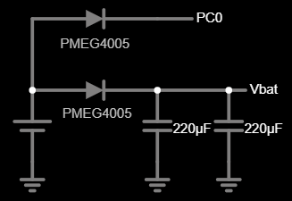
![]()
When power is lost, the voltage at MCU's pin PC0 goes to 0, triggering the shutdown sequence. The power for shutdown is provided by the capacitors. The upper diode is only for reverse polarity protection, bottom diode also prevents current from flowing from the capacitors to PC0.
Now let's save the data to EEPROM. Its access granularity is 4 bytes, so it's rational to have a data structure with a size, multiple to 4 bytes. We need to save the total accumulated dose and total measurement time: seconds, minutes, hours and days (up to 999). I've managed to cram the data into an 8-byte structure by removing the redundant bits in variables that we need to save:
struct {
  uint16_t ddisp:10;  // displayed digits of dose, 0..999
  uint16_t min:6;     // dose measurement minutes, 0..59
  uint16_t mode:3;    // dose display mode, 0..6
  uint16_t hrs:5;     // dose measurement hours, 0..23
  uint16_t dose_h:8;
  uint16_t dose_l:16; // radiation events counter, 0..11538461
  uint16_t days:10;   // dose measurement days, 0..999
  uint16_t sec:6;     // dose measurement seconds, 0..59
}state;
Notice that the bit order is such that the structure can be split into 4 bytes during write operation. During shutdown, the data is packed into this structure and written to EEPROM, and then unpacked during startup and the value of respective variables is restored.
-
Counting radiation events
10/07/2022 at 01:49 • 0 commentsReading signals from a Geiger tube
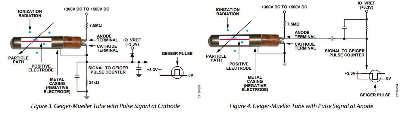
There are two ways to read the signal — from the anode and from the cathode of the tube:
![]()
Two types of Geiger tube readout circuits (source: CN-0536 by Analog Devices) I'll be reading signals from the anode because it's more convenient to route the PCB this way and this approach provides more immunity to electrical noise. In case of anode readout, the main goal is to reduce the pulse amplitude, so it doesn't destroy the MCU. The schematic is as follows:
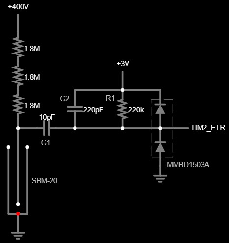
![]()
C1 and C2 act as a capacitive divider, attenuating pulse amplitude. C1 must be rated for more than 400V, I'm using a 2kV rated one. R1 is just a pull-up resistor: because the pulse is negative going, the idle voltage level should be high. I am deliberately not using MCU's internal pull-up resistor here because its value is too low, and it will shorten the pulse too much because of that. The diodes are used to clip the pulse amplitude to a safe level. Let's see how the output pulse will look like when a Geiger tube registers a radiation event:
![]()
The output pulse swings from supply to ground with some overshoot due to voltage drop in diodes. High amplitude of the pulse allows us to use a digital input to register it.
Making loud clicks
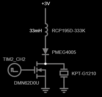
I would like to be able to hear when a radiation event is registered, and I want it loud. There are two types of sound transducers — magnetic and piezoelectric. Magnetic ones require high current, so they're out of the question, also they're not that loud compared to piezoelectric. The problem with piezoelectric transducers is that they require high voltage to produce a loud sound, so we need the means to generate high voltage pulses. Here's what I came up with:
![]()
This circuit works similar to a boost converter. When the transistor is open, the inductor starts building up current and the remaining charge in the transducer is removed to increase voltage swing across it (electrically they behave like capacitors, so they can hold some charge). When the transistor closes, the energy that the inductor had at that time, is transferred into transducer's capacitance and it stays there until the next cycle. I've created a simulation if you want to take a closer look at the circuit's operation.
I'm using a KPT-G1210 transducer, it's rated for 30V, so let's generate voltage somewhere in this vicinity. As I said before, the energy EL held by an inductor is transferred into transducer's capacitance:
where:
- Et — energy, held by transducer's capacitance
- L — inductance value
- IL(pk) — peak inductor current
- Ct — transducer's capacitance
- Vt — voltage that the transducer will build up
From the formula above we get:
where
In this case, Ra is the sum of inductor's series resistance and MOSFET's drain-source resistance. We can control two parameters in this circuit — the inductor value and its charging time tON. I've selected a 33mH inductor to reduce its peak current; LR44 battery has high ESR, so if we pull too much current from it, we may get brownouts at low battery levels. This leaves us only with the tON to figure.
We'll be using a TIM2 timer in the MCU to generate pulses. It has a one-shot mode and an external trigger, so we'll set it to produce a single pulse of fixed length when its trigger input TIM2_ETR detects a falling edge from the Geiger tube. I've added this code to the TIM_Init() function:
  /* TIM2 SETUP (ONE-PULSE MODE, EXT. TRIGGER) */
  PB_DDR_bit.DDR2 = 1;         // Set PB2 as output (TIM2_CH2)
  PB_CR1_bit.C12 = 1;          // Set PB2 as push-pull
  CLK_PCKENR1_bit.PCKEN10 = 1; // Enable TIM2 clock
  TIM2_ARRH = 0;
  TIM2_ARRL = 6;           // Pulse length = 30.52uS * TIM2_ARRL
  TIM2_CCR2H = 0;
  TIM2_CCR2L = 1;
  TIM2_CCMR2_bit.OC2M = 7; // PWM mode 2
  TIM2_CR1_bit.OPM  = 1;   // One-pulse mode

  TIM2_SMCR_bit.TS  = 7;   // Trigger source - external
  TIM2_ETR_bit.ETP  = 1;   // Trigger on falling edge
  TIM2_SMCR_bit.SMS = 6;   // Start the timer on ext. trigger
  TIM2_CR2_bit.MMS = 2;    // Update event -> trigger output

  TIM2_CCER1_bit.CC2E = 1; // Enable channel 2 output
  TIM2_BKR_bit.MOE = 1;    // Enable main output
The length of the pulse that this timer generates, can only be a multiple of its clock period: 1 / 32.768 kHz = 30.52 µS. Let's see what voltage we'll get with a pulse that's 6 clock periods long — 183.1 µS.
Let's see what we'll get in practice.
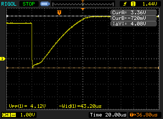
![]()
Close enough, 27V, and the MCU generates a pulse of correct length as well. The oscillation after the pulse is because the transducer continues to vibrate after making a clicking sound, generating voltage. Now let's hear how the clicks sound like.
Hackaday didn't let me embed a video from Imgur, so here's a link to it. The video shows a completed device but the clicking will work with the code and circuits provided so far.
This is actually quite loud for such a small transducer; I can easily hear the clicks from another room.
Counting radiation events
Just having a clicking dosimeter isn't enough, there should be quantitative measurements. To make these measurements, we should somehow count the radiation events. And since we have another timer to spare, we'll use it for this. We will set timer TIM3 to increment its counter whenever it sees that TIM2 produced a pulse.
  /* TIM3 SETUP (TIM2's PULSE COUNTER) */
  CLK_PCKENR1_bit.PCKEN11 = 1; // Enable TIM3 clock
  TIM3_SMCR_bit.TS  = 3;       // Trigger source - TIM2
  TIM3_SMCR_bit.SMS = 7;       // Trigger increments timer's counter
  TIM3_CR1_bit.CEN = 1;        // Start the timer
This works independently from the CPU as well, so we can read the quantity of registered radiation events whenever we want.
-
Boosting voltage
10/03/2022 at 16:19 • 0 commentsTowards efficient boost converter architecture
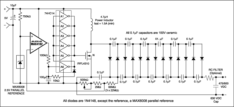
Most DIY Geiger counters that I've seen on the Internet have very simple architecture: just an oscillator driving a transistor, sometimes with Zener diodes to limit the output voltage. This approach is inefficient, so I've decided to make a boost converter that's both efficient and compact. The first thing that comes to mind is that the converter has to disable the oscillator when it's not needed. This approach is described in an appnote by Maxim Integrated:
![]()
Here they're using a comparator to control the oscillator output: when the feedback voltage is less than the reference voltage the oscillator is enabled, and vice versa. Since a Geiger tube only consumes energy when hit by a particle, the oscillator shall remain idle most of the time, and that saves a lot of power. Also there's a 6-stage voltage multiplier, so we can feed the lower output voltage from its first stage to a feedback divider, thus minimizing the current through it. I'll be reducing losses in the feedback divider as much as possible since it consumes the most power in the circuit above.
Setting up the microcontroller
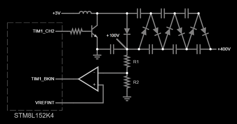
One huge benefit of microcontrollers is that they have peripherals that can replace discrete components, saving power and PCB space. In our case we can use a microcontroller to replace a voltage reference and an oscillator in the circuit above (and even a comparator if we wouldn't have to drive a 4-backplane LCD).
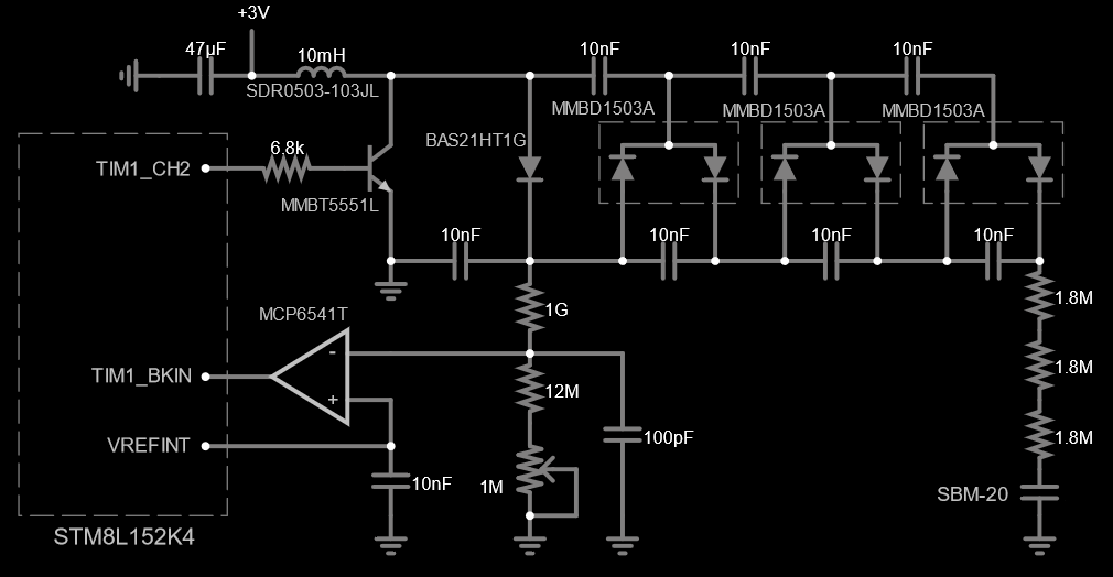
We should set the MCU to output a reference voltage and a comparator-controlled PWM: when the comparator output is LOW (voltage divider voltage less than reference voltage), the timer generates PWM, otherwise it sets its output to LOW, closing the transistor. The only timer that we can use is TIM1 because pins, tied to other timers are needed for other functions. This timer has a break input which disables timer's output when it receives a signal, which is exactly what we need. The schematic is as follows:
![]()
To use a lower value inductor for better energy and space efficiency, we'll set the PWM generation for shortest positive pulse possible, i.e. highest frequency and lowest duty cycle; the best we can get with a timer is half the system clock. The MCU is clocked from 32.768 kHz crystal, which means 50% duty cycle PWM at 16.384 kHz.
To write the code I'll be using the IAR Embedded Workbench for STM8.
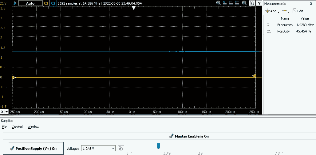
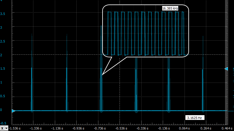
#include "iostm8l152k4.h"

void Clock_Init(void)
{
  CLK_SWCR_bit.SWEN = 1;         // Prepare to change the clock source
  CLK_SWR = 0x08;                // Change the clock source to LSE
  while(CLK_SWCR_bit.SWBSY==1);  // Wait until it starts up
  CLK_CKDIVR = 0x00;             // Change the clock prescaler from default /8 to /1
  CLK_ICKCR_bit.HSION = 0;
  CLK_ICKCR_bit.LSION = 0;       // Disable internal oscillators
}

void VREF_Init(void)
{
  while(!PWR_CSR2_bit.VREFINTF); // Wait for voltage reference to stabilize

  CLK_PCKENR2_bit.PCKEN25 = 1; // Enable clock for COMP peripheral
  COMP_CSR5_bit.VREFTRIG  = 2; // Disable Schmitt trigger on PD7 to reduce leakage
  COMP_CSR3_bit.VREFOUTEN = 1; // Enable VREF output
  RI_IOSR2_bit.CH8E = 1;       // Connect VREFOUT to PD7
  CLK_PCKENR2_bit.PCKEN25 = 0; // Disable clock for COMP, was only needed for init
}

void TIM_Init(void)
{
  /* TIM1 SETUP (SYSCLK/2 GATED BY EXTERNAL SIGNAL) */
  PD_DDR_bit.DDR4 = 1;         // Set PD4 to output mode
  PD_CR1_bit.C14 = 1;          // Set PD4 output to push-pull mode
  CLK_PCKENR2_bit.PCKEN21 = 1; // Enable TIM1 clock

  TIM1_ARRH = 0;
  TIM1_ARRL = 1;        // Highest frequency (16.384 kHz)
  TIM1_CCR2H = 0;
  TIM1_CCR2L = 1;       // Lowest duty cycle (50%)

  TIM1_BKR_bit.BKE = 1;      // Enable output break
  TIM1_CCMR2_bit.OC2M = 0x6; // Set output mode: PWM mode 1
  TIM1_CR1_bit.CEN = 1;      // Enable timer counter
  TIM1_CCER1_bit.CC2E = 1;   // Enable TIM1_CH2 output
  TIM1_BKR_bit.AOE = 1;      // Automatically recover from output break
}

int main(void)
{
  Clock_Init();
  VREF_Init();
  TIM_Init();
}
The beauty of this approach is that it's completely core independent — notice that that there is no code after initialization, the CPU isn't necessary to control the boost converter. Let's test if this works. I've connected a voltage source to the comparator's inverting terminal and the MCU should output PWM when the voltage is below reference (1.224V) and output LOW level otherwise:
![]()
Yellow trace — TIM1_CH2 output, Blue trace — voltage at comparator's inverting terminal Seems to work fine, let's move to the analog part of the boost converter.
Selecting components
Feedback resistors and voltage multiplication
As I've said, the feedback network (R1 and R2 on the circuit above) can easily be the biggest energy consumer in the whole circuit, so we should use resistors of the highest value and have the lowest feedback voltage possible. Feedback voltage depends on the number of multiplication stages. Initially I've built a booster with x12 multiplier but it had a parasitic oscillation issue which I failed to resolve.
![]()
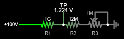
Failed booster with a 12-stage multiplier I ended up with the x4 multiplier (as shown on the circuit above) which is compact and has reasonably low current consumption. We have to supply 400V to an SBM-20 tube, so the feedback voltage at the first multiplication stage shall be 400V / 4 = 100V. At this input voltage, the feedback divider output voltage should be equal to VREF — 1.224V.
I've got my hands on some 1GΩ resistors, so I'll use them for R1. Then R2 = 12.4MΩ. Resistors of this value are not available, so I've split it into a 12MΩ resistor and 1MΩ potentiometer, which will also allow to compensate for R1 and VREF tolerances:
![]()
Using a 100V for output feedback may seem horribly inefficient but let's calculate how much battery current the boost converter shall actually consume to drive the feedback network. For this we should write equations for the power consumed on both sides of the converter (low voltage side and high voltage side):
From this we can derive the battery current, consumed by the booster's feedback loop:
Of course, the real-world value will be higher because the efficiency of the boost converter is less than 100%. Also at lower battery voltages the current consumption will increase: 5.5µA at 1.8V (lowest operating voltage for the MCU). Still, I consider this acceptable, given that the total consumption of the device is 44µA at full battery and normal background radiation level.
Comparator
Since we are using very high value resistors, we should mind the load we put on the feedback voltage divider — the comparator must have a low input bias current (and a low quiescent current if we want long battery life). I'm using an MCP6541 comparator in this project because due to the chipageddon it was the only one available to me that met the requirements: 1pA input bias current, 600nA quiescent current. 3.3mV hysteresis is barely enough to provide enough noise immunity though, this is most likely the main reason I was unable to make a 12-stage voltage multiplier work. If I could, I'd use something like TLV7031 or TLV4051R1.
Inductor
Inductor selection directly influences the efficiency and maximum output power of the converter. I've chose SDR0503-103JL — 10mH inductor with 110Ω max series resistance because it was the highest value inductor available with reasonably small dimensions (I couldn't have an inductor with >3mm height). We want high inductance because of very low PWM frequency, and also high inductance reduces peak inductor current during converter operation which helps to reduce losses in a transistor, — high-voltage transistors don't handle high currents very well.
Let's see how much power our boost converter can provide with this inductor. To find it, we should find its peak current first. Current vs time formula for an inductor with series resistance is as follows:
where:
- VL — voltage applied to the inductor
- Ra — sum of resistances in inductor's current path: inductor series resistance, power supply ESR, transistor etc. For simplicity, I'll assume all resistances except inductor's negligible.
- L — inductance
To find the amount of energy, transferred during one PWM cycle, we should first find the current that the inductor builds up during transistor ON time (which will be its peak current). Our MCU outputs 16.384 kHz PWM with 50% duty cycle. Then:
where D — duty cycle. From this, the peak inductor current will be:
Here we're finding the peak current at the lowest supply voltage (1.8V) to find the worst case power output.
The energy, transferred during each PWM cycle is:
These energy transfers occur at 16.384 kHz rate, so maximum output power will be:
Now we will check if that's enough to drive the feedback divider and a Geiger tube. Feedback divider consumes:
With a Geiger tube things are more complicated. Given a fixed supply voltage, a Geiger tube consumes a fixed amount of charge during each registered event, however for some reason the amount of charge is not specified in datasheets. Fortunately, there is a rule of thumb: the tube consumes a charge, roughly equal to 1/3 of the total charge, held by tube's capacitance:
The maximum counting rate for an SBM-20 tube is 1400 CPS (Hz), so maximum consumed power will be:
This formula stems from definition of charge: Q = I ⋅ t, from this I = Q / t = Q ⋅ f.
So the total power, consumed by high-voltage part will be:As you can see, we have plenty of headroom even with fully discharged battery.
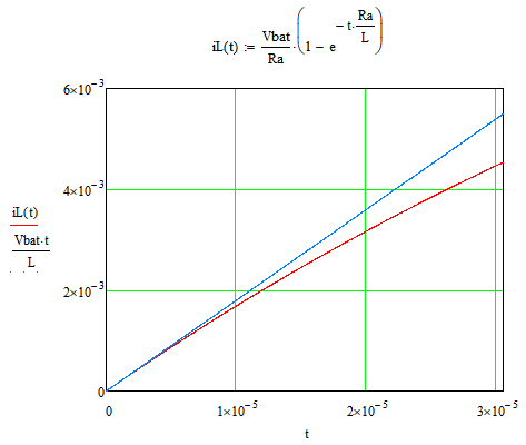
Now let's talk about efficiency. The series resistance of our inductor is 110Ω, this obviously will significantly reduce efficiency. A simple way to check the efficiency (and estimate optimal tON) for given inductor is to compare the iL(t) graphs for lossless and lossy inductor. A formula for ideal inductor stems from the basic inductor equation:
I'll plot the inductor currents from t = 0 to tON.
![]()
As we can see, as time increases, the graph of current in real inductor rises slower and slower, and eventually it will become a flat line because current will be limited by inductor's series resistance. Obviously, the more these graphs deviate from each other, the lower the efficiency will be. In our case, at t = tON, iL(real) / iL(ideal) = 0.85 (85%), so we're losing about 15% efficiency with this inductor. I think, this is acceptable, considering the small size of the inductor.
Transistor and its base resistor
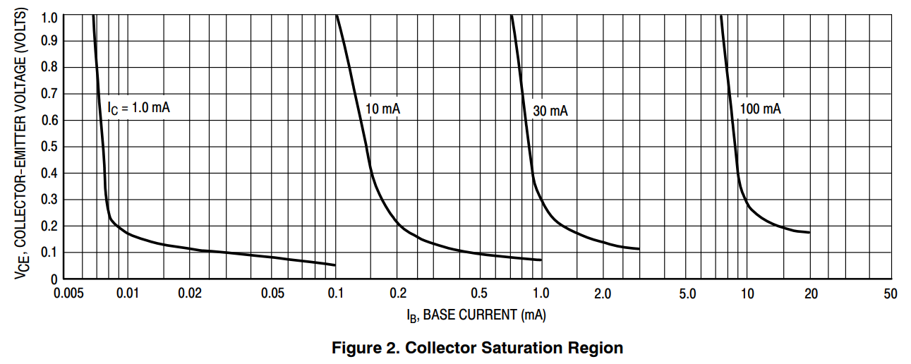
I was unable to find any suitable MOSFETs, so I resorted to bipolar transistors. And there's still not many to choose from: BCX41, BSR19A and MMBT5551 are the only ones I would use. I was able buy only the MMBT5551. There are two transistor parameters that I consider most important — collector leakage and collector-emitter saturation voltage at given collector and base currents.
Low leakage helps to reduce energy losses in the inductor, improving efficiency. The general idea to get low leakage is to have a big headroom in voltage rating . This transistor is rated for 160V, so we have 60V headroom.
![]()
Collector-emitter saturation voltage (VCEsat) is what causes energy losses in the transistor when it's open, so we want it to be as low as possible.
![]()
As you can see, VCEsat decreases as base current increases, so we should find a compromise between base current and VCEsat. The maximum collector current is equal to peak inductor current when the battery is at full capacity:
so we should use the second left graph to find the optimal base current Ib. The goal is to find Ib such that the sum of energy, lost on driving the base and energy, lost due to VCEsat, is minimal.
Energy, dissipated in every PWM cycle due to VCEsat:
This formula stems from definition of energy: E = P ⋅ t = VI ⋅ t. After integrating we get:
At this point we should take into account that the transistor will reduce the inductor voltage by VCEsat, which is reflected in formulas above.
Energy, dissipated in every PWM cycle to drive the transistor base is:
Here 0.7V is base-emitter voltage drop.
Now I'll just try various points on the graph and find the point with smallest Evce + Eb, which happens to be at Ib = 0.4 mA (with VCEsat = 0.1V and total loss being 35.3 nJ per cycle). Since we took this value from the graph for Ic = 10mA, we get:
Now if we substitute our peak inductor current for Ic, we'll get:
And then the base resistor will be:
Closest value from E24 series is 7.5kΩ but 6.8kΩ from E12 series will work fine as well.
Tube anode resistors
The datasheet for SBM-20 tube recommends a 5.1MΩ anode resistor. Since we're optimizing the PCB size, we have to use small components. In our case we can use three SMD 0805 resistors in series: most of them are rated for 150V, so three of them should withstand 450V (given they have same value). If we use 1.8MΩ resistors, we'll get 5.4MΩ. which is close enough. At the last moment I realized I only have 2.2MΩ resistors, so I've used those and they work fine.
Diodes and capacitors for voltage multiplier
We are interested in three things here: appropriate voltage rating, low leakage and small footprint. In our case, components in voltage multiplier must be rated at least for the feedback voltage: 100V. Not double that, like most articles about voltage multipliers tell. In our case, the input voltage swings from 0V to 100V, not from -100V to 100V like these articles assume.
There are plenty of suitable diodes and capacitors, I've chose BAS21 and MMBD1503A diodes because they have small footprint and 10nF / 500V, SMD 0805 capacitors to have a reasonable voltage headroom to avoid capacitance derating. Some of you might ask if 10nF capacitors are enough to provide sufficient power for a Geiger tube. The equivalent output resistance of a voltage multiplier given all its capacitors are the same value is:
where n — number of multiplication stages. Obviously, this is more than enough to drive a 5.4MΩ anode resistor.
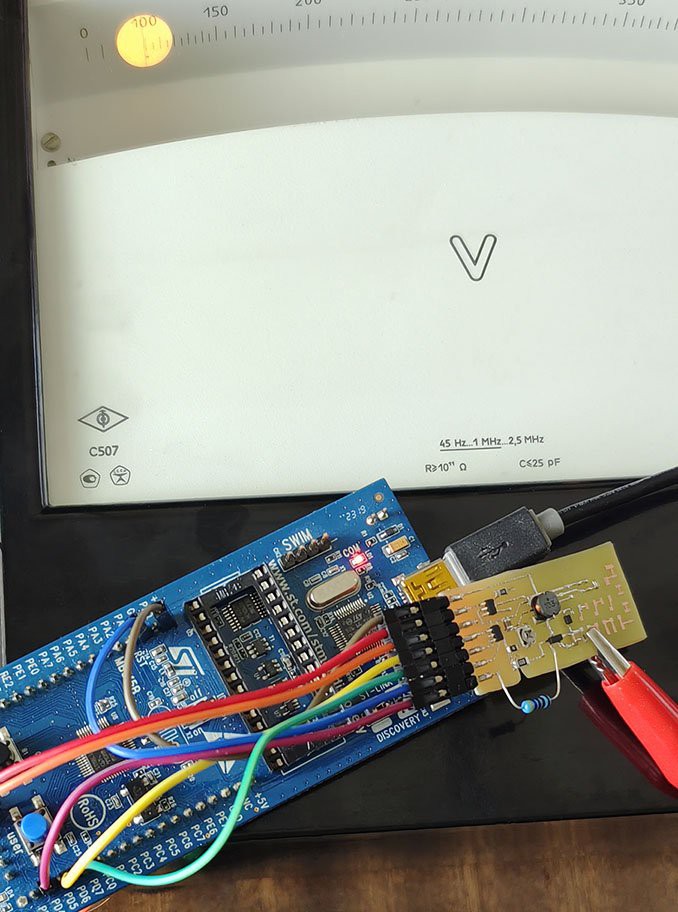
Testing and debuggingI've made a crude prototype to test the operation of my boost converter. I forgot to make proper photos, so here's one without voltage multiplier, — I was testing if the boost converter correctly outputs 100V, and it does. I was using STM8L-DISCOVERY board for software prototyping.
![]()
Notice that I am using an electrostatic voltmeter to measure the voltage because a regular multimeter will overload the boost converter and thus show a voltage, lower than the converter would output without multimeter leads connected. This voltmeter has 100GΩ input resistance, so it doesn't affect the operation of the boost converter. Also notice a small cutout on the bottom left of the PCB. I made it to reduce PCB leakage under the 1GΩ resistor which may reduce its effective resistance.
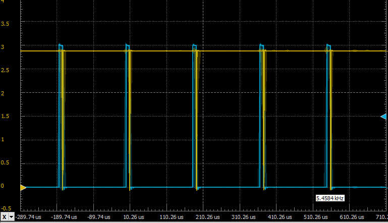
While the converter has correct output voltage, there was a problem — it was consuming a whopping 110µA current. I hooked the oscilloscope to the PWM output and comparator output and saw this:
![]()
TIM1_CH2 output (blue trace), comparator output (yellow trace) This looks nothing like a 16.384 kHz PWM with 50% duty cycle that we expect the MCU to generate, and it acts like this because the comparator sends very short breaking pulses to the MCU, which in turn makes PWM pulses much shorter than intended. Because of that, to maintain voltage, the MCU has to generate PWM almost non-stop because with such short positive pulses the converter cannot push too much power, and to make matters worse, the transistor doesn't even have time to fully open. Also fun fact, the oscillation occurs at 5.458 kHz which is exactly 3 times lower than 16.384 kHz. Go figure why that is.
Then I looked at VREF and saw this:
![]()
Yellow trace - comparator output, Blue trace - VREF ripple This is getting more and more weird. How can a comparator with 1pA input bias current load the VREF output so much that it causes 0.75V ripple on it?! I've tried replacing the comparator, to no avail. Guess I just got a bad batch of these comparators. Also apparently the oscilloscope loaded VREF output more than it could handle (it can't output more than 1 µA) and this shifted the oscillation frequency.
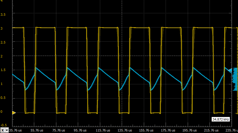
First thing that came to mind — bypass the VREF with a 10nF capacitor. This indeed reduced VREF ripple to ±1 mV (which I think is a lot for such a large capacitor and light load) but did not solve the oscillation problem at all. Then I assumed that the same thing happens on the feedback side and decided to bypass the feedback divider output as well. I couldn't just use whatever capacitor I wanted there because as capacitance increases, the leakage current increases as well and since we have a 1GΩ resistor in the feedback divider, at some point the leakage current of a bypass capacitor may become significant. So I've started with a small value — 10pF and started increasing it until the parasitic oscillation was gone, at 100pF. A healthy boost converter drives a transistor like this:
![]()
Now the converter consumes 7µA when idle (MCU consumption not included, just inductor+comparator) and I'm happy with this number. The final schematic is as follows:
![]()
And, of course, the final test — for the output voltage after multiplication.
![]()
Compact, low-power Geiger counter
A marker pen sized Geiger counter with up to 12 months battery life from 2xLR44, based on STM8L152K4 microcontroller