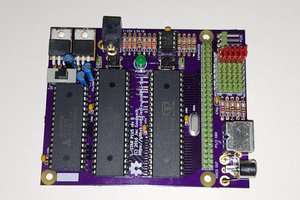
Modifications:
- Low-height crystal is less vulnerable to knocks
- Uses FTDI TTL-to-USB cable instead of MAX232 chip and capacitors
- PC104 expansion connector
Stuart Conner's Simple TMS9995 board build
To make the experience fit your profile, pick a username and tell us what interests you.
We found and based on your interests.
Modifications:
TMS9995_EVMBUG_FORTH_BASIC.txtA file you can assemble online to get the 64K switch-selectable FORTH/BASIC firmware.plain - 237.63 kB - 10/12/2022 at 19:27 |
|
|
TMS9995-ROM.txt.bin64K ROM image with Forth then BASIC, so one can select by switching during reset.octet-stream - 64.00 kB - 10/11/2022 at 23:37 |
|
These might be useful as a source of example programs. Most of them rely on graphics, or Cortex hardware, so few are good for my text-only board. Oh well, at least this index will be of interest to Cortex users.
Issues 1, 5 and 8 have not appeared on the internet yet.
Not available yet
ETI Cortex Users Group News Letter 2
ETI Cortex Users Group News Letter 3
ETI Cortex Users Group News Letter 4
Not available yet
ETI Cortex Users Group News Letter 6
ETI Cortex Users Group News Letter 7
Not available yet
ETI Cortex Users Group News Letter 9
ETI Cortex Users Group News Letter 10
ETI Cortex Users Group News Letter 11
ETI Cortex Users Group News Letter 12
ETI Cortex Users Group News Letter 13
ETI Cortex Users Group News Letter 14
ETI Cortex Users Group News Letter 15
ETI Cortex Users Group News Letter 16
nc | 1 | 40 | A15/CRUOUT |
nc | 2 | 39 | A14 |
CLKOUT | 3 | 38 | A13 |
D7 | 4 | 37 | A12 |
D6 | 5 | 36 | A11 |
D5 | 6 | 35 | A10 |
D4 | 7 | 34 | A9 |
D3 | 8 | 33 | A8 |
D2 | 9 | 32 | A7 |
VCC | 10 | 31 | VSS |
D1 | 11 | 30 | A6 |
D0 | 12 | 29 | A5 |
CRUIN | 13 | 28 | A4 |
!INT4/EC | 14 | 27 | A3 |
!INT1 | 15 | 26 | A2 |
IAQ/HOLDA | 16 | 25 | A1 |
!DBIN | 17 | 24 | A0 |
!HOLD | 18 | 23 | READY |
!WE/!CRUCLK | 19 | 22 | !RESET |
!MEMEN | 20 | 21 | !NMI |
Pinout matches the TMS9995 CPU apart from pins 1 and 2 which are connected to the crystal on the CPU. If you wanted to drive the CPU from an external clock source, then you could wire pin 2 from the connector to the CPU.
A0...15 are like A15...0 of the Z80 !MEMEN is like !MREQ of the Z80 !WE is like !WR of the Z80 !DBIN is like !RD of the Z80 !HOLD is like !BUSRQ of the Z80 HOLDA is like !BUSAK of the Z80 (but inverted) READY is like !WAIT of the Z80
The signal names look strange at first but have conventional equivalents.
The TMS9995 is an extremely quirky processor.
The Communication Register Unit interface is arguably the weirdest feature. It is a serial I/O interface to peripheral chips.
Memory space is byte-addressable, but CRU space is bit-addressable. A desired device is accessed by placing its software base address in Register 12 and exercising the CRU commands.
The CRU bit-space is 32K bits, because the least-significant address bit is used to send a data bit to the peripheral.
The bit address is incremented when transferring multiple bits to/from a device.
I can see this has some advantages; for an 8-bit output port you would only need 3 address signals and 1 data signal, four in total instead of 8 data bits. It also simplifies bit operations, as there is no need to AND/OR bytes to manipulate single bits. The reduction of signal pins explains how they can get a full UART into a DIP18 package.
On the other hand, the disadvantages are that the scheme is unique to the TMS 9000 family. No other CPU uses it, so there is little demand for it.
I would like to add some more conventional devices as memory-mapped I/O. This will require modifying the address decoder to have "holes" in memory space.
Pin 1 isolated from 5V, then wired to A14 (pin 1 of RAM)
Pin 27 isolated from A14 (pin 1 of RAM), then wired to /WE (pin 27 of RAM).
Cut track on top side of board, from ROM pin 1 to pin 28 (VCC):
Next make the mods shown below:
The RAM is on the left, the ROM on the right. Note:
ROM pin 27 track cuts each side.
The track joining pins 1 joins the A14 track.
The ROM pin 27 is tied to RAM pin 28 (VCC), not 27 (/WE). The latter connection will cause the CPU to corrupt the ROM even if the code never tries to write to EEPROM addresses.
The DIP28 socket is wired for a 32K EPROM.
I prefer EEPROM because few people want to be bothered with UV erasers. I could mod the socket but would be limited to 32K. An alternative is to modify the socket so that pin 1 is switchable high or low, so that I can select either BASIC and FORTH using a 64K EPROM. Pin 1 is A15 on the chip, and VCC by default on the PCB, so I will put the standard BASIC in the second half of a 64K EPROM.
I have many 64K EPROM chips (type 27512). I don't plan to modify the firmware much, if at all, so I will not be bothered by UV erasure.
Links to ROM images:
EVMBUG system monitor and BASIC (32K)
EVMBUG system monitor and FORTH (11.5 K)
The latter not being 32K, I cannot simple catenate them into one 64K file, so I shall simply join them at the ROM-programming stage.
2022-10-15
Programmed a 32K EEPROM AT28C256 with the monitor and BASIC.
Modified EPROM socket for 32K EEPROM
2022-11-21
TMS9902 fitted, but no serial I/O seen.
2022-11-24
EEPROM socket pin 27 changed from /WR to VCC. May have been corrupted, so I reprogrammed it. Got partly garbage characters with the common 9600-8-N-1 setting. Followed web page and set it to 9600-7-E-2 setting. Success, the sign-on message appeared!
Firmware is now working.
The L suffix of the HM62256L indicating "low power" refers the the standby current. In normal operation, it consumes as much power as the normal-power part. The power is 40 milliwatts at 1 MHz, which is 8 mA at 5 volts. However, the current-frequency graph indicates a linear relationship. The 85 ns part consumes 100% of 70 mA at full speed (10 MHz) and about 25% (17 mA) at 2 MHz. A TMS9995 with 12 MHz crystal has a 3 MHz cycle rate which sets an upper bound of around 23 mA.
The currents above exceed the 100 mA of the minimum power USB peripheral, so I have not joined the VCC rail to the VCC of the USB cable connector.
2020-04-25
Soldered on the simple 9995 board:
2022
2022-09-30
2022-10-15
2022-10-15
2022-11-21
TMS9902 fitted, but no serial I/O seen.
2022-11-24
EEPROM socket pin 27 changed from /WR to VCC. May have been corrupted, so I reprogrammed it. Got partly garbage characters with the common 9600-8-N-1 setting. Followed web page and set it to 9600-7-E-2 setting. Success, the sign-on message appeared.
2022-11-26
115200 is the highest baud rate. It copes with a low character rate, and accepted my typing
10 PRINT "HELLO WORLD! "
20 GOTO 10
but when I copied and pasted the same text, I got
0 RT"EOWRD" 0GT 0
which shows it cannot process incoming text at that rate.
At 9600 baud, I got
10 PRT "HELO WORLD "
which is a little better. At 4800 baud:
10 PRINT "HELLO WORLD! "
0 GOTO 0
At 1200 baud:
10 PRINT "HELLO ORLD! "
2 GOTO 10
Even at 300 baud, characters are missed. It clearly needs flow control, but RTS and CTS are joined at the UART.
Stuart Conner said that most terminal programs let you set inter-character and inter-line transmit delays. However, the 300 baud rate slows the character rate to around 30 characters per second which is 33 ms each. That should be plenty of time.
Characters are missing in the middle of lines, when the CPU has nothing to do but put them in a buffer. It is not due to the CPU taking a long time to parse a line of BASIC.
The software solution would be to modify the firmware to have interrupt-driven serial input, so that characters would be buffered as fast as they came in, but it will take me a long time to modify code for a CPU I have no experience of. I'd have to add CTS/RTS handshaking but FTDI USB cables don't stop sending bytes until up to 3 bytes after being told to stop.
My favoured solution would be to get the CPU talking to an FTDI USB FIFO module. No baud rate hassles, not RS232 voltages and buffers, and dead easy to interface.
Create an account to leave a comment. Already have an account? Log In.
Become a member to follow this project and never miss any updates