Hardware Controlled 4 bit CPU
A hardware controlled 4 bit CPU based on lessons learnt from the TD4 and the CHUMP CPUs
A hardware controlled 4 bit CPU based on lessons learnt from the TD4 and the CHUMP CPUs
To make the experience fit your profile, pick a username and tell us what interests you.
We found and based on your interests.
ALUV6.pngPortable Network Graphics (PNG) - 25.36 kB - 12/27/2022 at 00:22 |
|
|
4BitV6.pngPortable Network Graphics (PNG) - 35.59 kB - 12/27/2022 at 00:22 |
|
|
CTRLV6.pngPortable Network Graphics (PNG) - 14.66 kB - 12/27/2022 at 00:22 |
|
|
IOV6.pngPortable Network Graphics (PNG) - 10.55 kB - 12/27/2022 at 00:22 |
|
|
PCV6.pngPortable Network Graphics (PNG) - 7.90 kB - 12/27/2022 at 00:22 |
|
|
A Virtual PCB
At least that is how I explained it to my partner!
It seems as if FPGA boards are pretty rare, almost all the main suppliers are out of stock, but I did find a Tang Nano 9k on ebay in Australia. So that is what I will use.
Gowin (the FPGA manufacture) has a free and no licence educational version of the IDE for the Tang Nano (only 382 Mb) which works except for the bit stream uploader. Checking the Internet, for Linux there is no solution except for the third party programmer: openFGPALoader. Found instructions to compile openFPGALoader and it works fine. Of note, openFPGALoader's command line arguments are human readable.
So next is to learn Verilog, but I will cheat and download a 74xxx library. But one thing I noted is that the list of implemented logic gates avoids those with tri-state outputs?
Checking the Internet, it is strongly recommended not to use tri-state outputs as FPGA capacity to model them is quite limited. So okay I will redesign the 4 Bit CPU to use multiplexers:
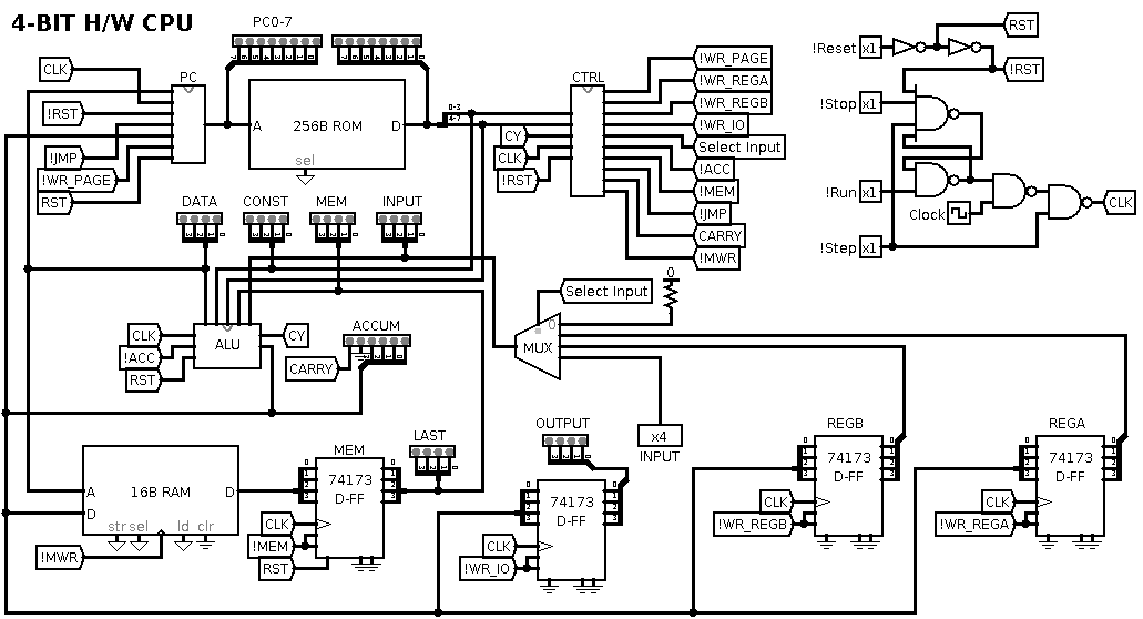
I changed the opcodes to suit the multiplexer, here is the control unit:
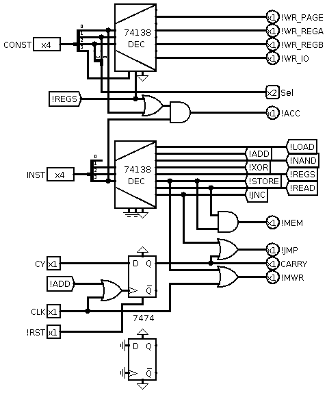
I will have to swap the 74173 with a 74377 reduced to 4 bits.
I will have to study the Gowin IP with regard to BROM and BRAM.
74xxx Verilog Code
Although I am not familiar with the syntax of Verilog, the 74xxx code is very easy to understand.
There appears to be option with regard to ROM/RAM, you can roll your own or use the specialised RAM on chip. I have to review:
TBC ...
AlanX
PCB Assembly
I have started assembly of the PCBs but I am waiting on a part.
Instruction Set
I have had time to think about improving the instruction set.
The idea came from the number of steps required to swap out the accumulator to memory. Better if I have a register and a swap opcode.
The idea actually frees up the opcode space as I can use the opcode "data" to specify the register and the registers can serve other purposes (e.g. the page register).
I need to look at how the memory data flow works as well.
Rebuilding the Micro-Architecture
I took the well published academic RISC micro-architecture:

And derived the CHUMP micro-architecture:
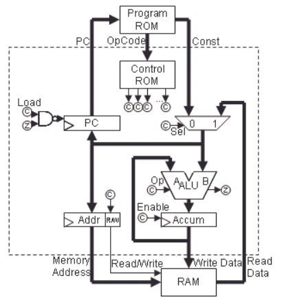
But along the way I saw an alternative memory arrangement:
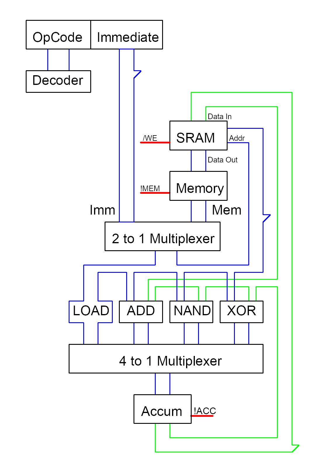
This configuration has three benefits:
I have tested the new micro-architecture in Logic-Sim (and it works fine.
Adding Registers to the CPU
This allows the inclusion of register read/write logic:

In the above drawing I will probably keep the old PC and JNC logic.
Now I can replace the Page opcode with a register(s) read/write opcode.
Working LogiSim Version 7
Have been working on the Version 7, it now has register read/write opcodes. Added four registers of the eight available slots:
Swapped the Page opcodes (Ex/Fx) with JNC opcodes (8x/9x).
Replaced the new 8x/9x opcodes with 8r/9r were r is a register constant or memory reference:
Here is the Top Level:

The Control Unit:
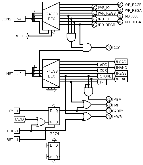
The ALU:

And the PC:

Overall a pretty significant improvements on CHUMP V5 and the 4 Bit CPU V6.
Here is the test code (the multiply algorithm):

This algorithm uses the new JNC and REGs opcodes, and multiplies F x E (13 x 14), the result is D2 (210).
Parts have Arrived
The parts have arrived. Finished off one of the Diode ROM boards, next is the CPU board:

TBC ...
AlanX
Version 6
Version 6 is like version 5 except the expanded ALU is not used. Here are the op codes:

I wrote up an 8 bit multiplication routine, first in C:
#include <stdio.h>
#include <stdlib.h>
#include <stdint.h>

unsigned short mul(unsigned char A,unsigned char B)
{
  // Returns:
  //   A = A * B
  unsigned short res=0;
  unsigned char i=8;  // 8 bit

  LOOP:
    res=res+res;
    if (A>=0x80) {
      res=res+B;
    }
    A=A+A;
    i=i-1;
  if (i>0) goto LOOP;
  return res;
}

int main(void)
{
  unsigned char A,B;
  unsigned short M;
  int i,j;


  for (i=0;i<=255;i++) {
    for (j=0;j<=255;j++) {
      A=(unsigned char)i;
      B=(unsigned char)j;
      M=mul(A,B);
      if (i*j!=M) printf("%6d %6d\n",i*j,M);
    }
  }

  return 0;
}
I tested all cases so I know it works. I then dumbed it down to 4 bits:
unsigned short mult(unsigned char A,unsigned char B)
{
  // Returns:
  //   C = A * B
  unsigned short C=0;
  unsigned char D=4;  // 4 bit

  LOOP:
    C=(C+C)&0X0F;     // 4 bit adjustment
    if (A>=8) {       // MSB of 4 bit
      C=(C+B)&0X0F;   // 4 bit adjustment
    }
    A=(A+A)&0X0F;     // 4 bit adjustment
    D=(D-1)&0X0F;     // 4 bit adjustment
  if (D>0) goto LOOP; // 4 bit adjustment
  return C;
}

int main(void)
{
  unsigned char A,B;
  unsigned short C;

  A=(unsigned char)5;
  B=(unsigned char)3;
  C=mult(A,B);
  printf("C=5*3 %d\n",C);
  return 0;
}
Although the code handles overflow into the high order bit of the result variable (C), in this implementation, I have not considered overflow of C. Therefore 3x5 is big as the algorithm can handle:
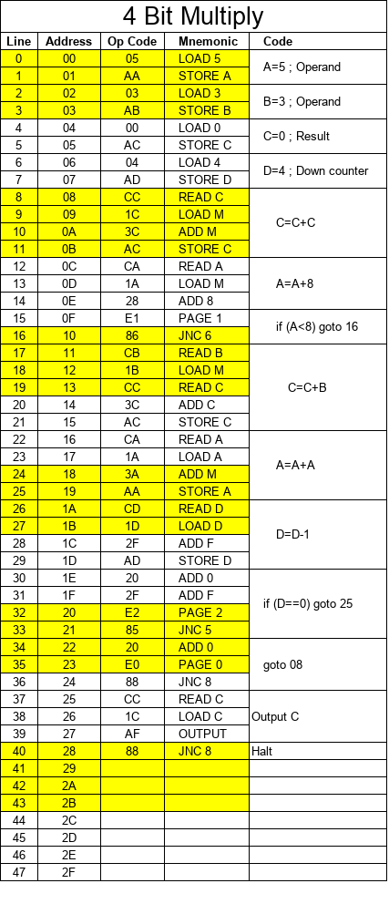
Here is the code running:

In the RAM window: A, B, C & D are updated as the program runs. At the end, the output port displays the answer.
The run starts with:
At the end:
Here is a version that handles lager numbers:

If you used A=13 (D) and B=15 (F), then the result would be C=3 and D=12 (C) or 195.
Refer to the Simulation below:
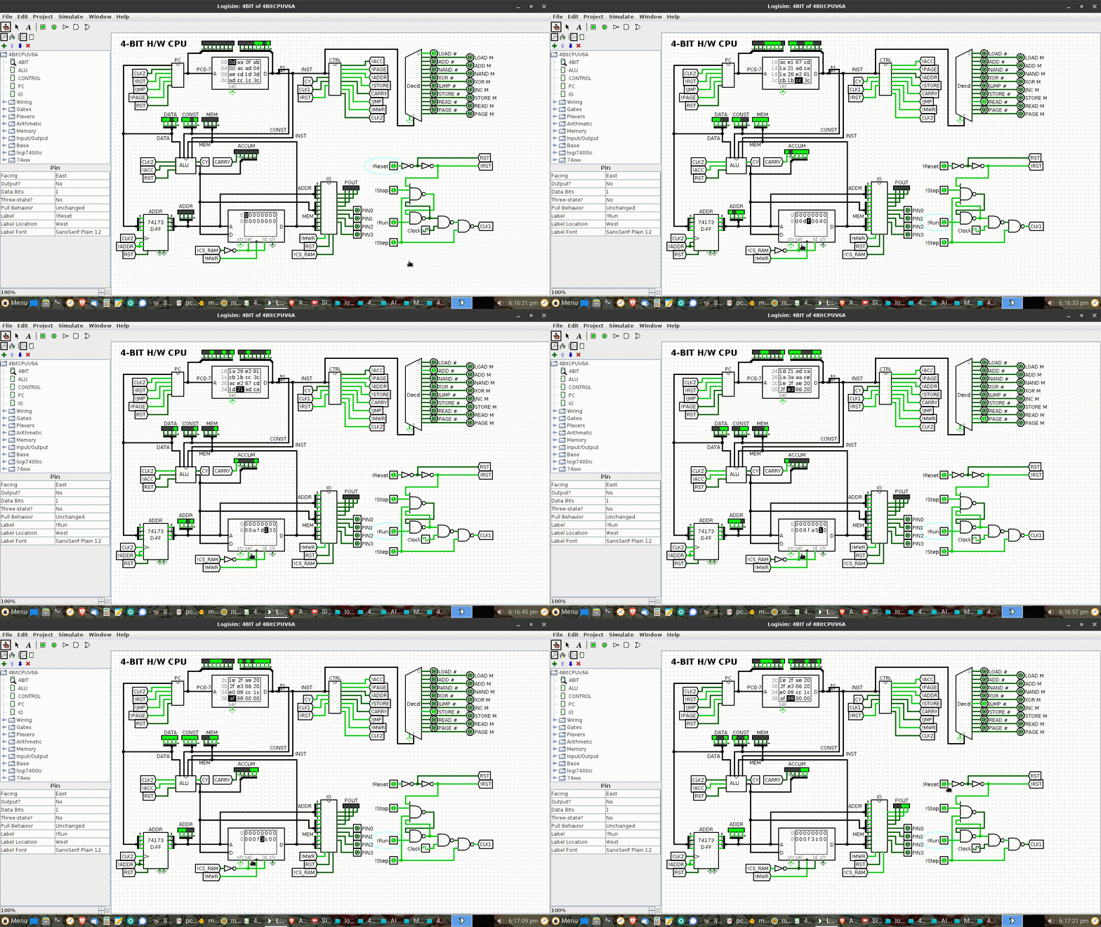
Unfortunately both of these programs are too big for my 32 byte PROM design.
I will check the schematic tomorrow for any missed errors.
Yeah, found two errors, fixed and forwarded for manufacture.
AlanX
Schematic and PCB
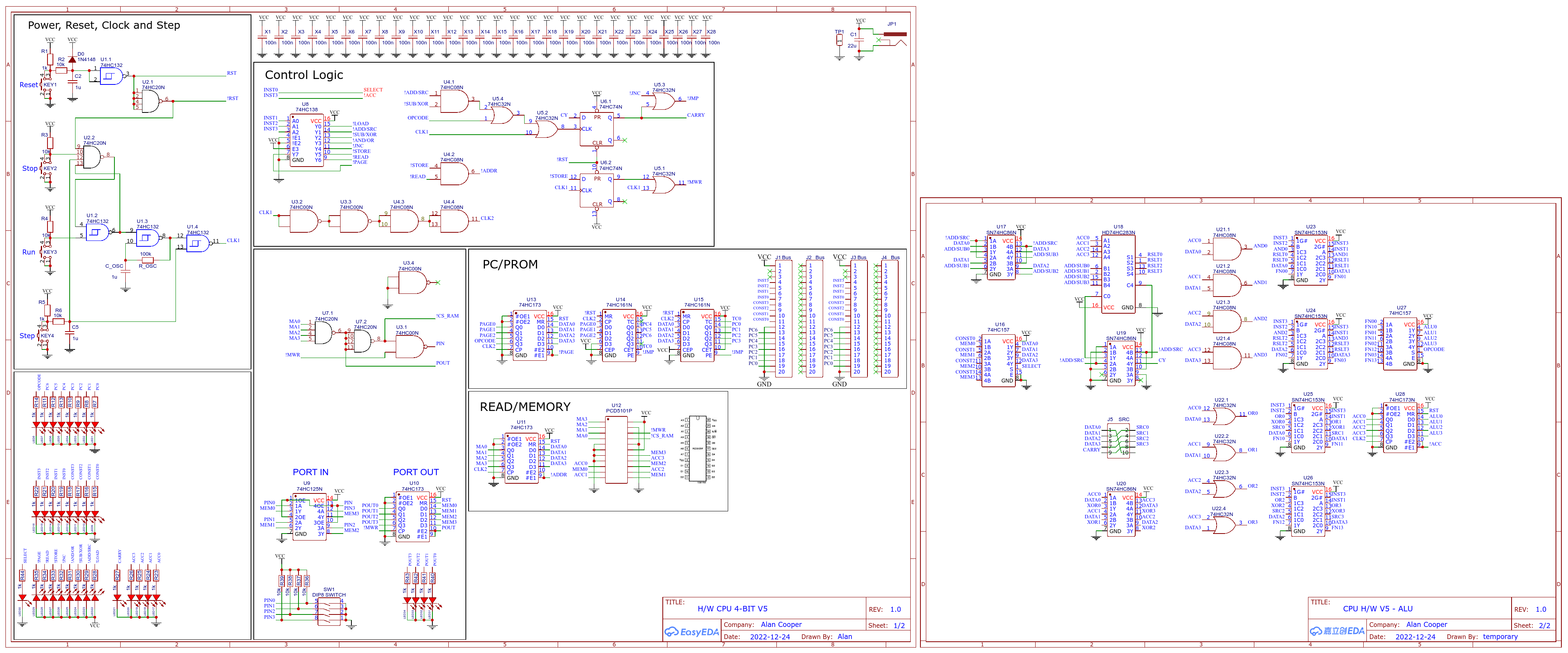
Started the schematic design, the ALU is pretty well all new, so it will take time.
The layout will be important as the auto-router will struggle with this many chips.
---
The 16 byte diode PROM boards arrived today. Two boards will have nearly 400 components, so they will take a while to solder.
---
Some updates to the simulation model.
---
Some progress on the schematic, trying to group the chips:
Instruction Set Again
The minimum instruction set is:
Missing are instructions like LEA, CALL and RTN, etc, but these require structural changes.
Subtraction is pretty easy to do, I will use reference variables here.
A = A SUB B:
Test if equal:
Test if bits are HIGH:
Test if bits are LOW:
Other logic gates can be derived from the NAND gate, but may require memory to store intermediate results. Although NAND can replace XOR in many cases, XOR is "necessary" for efficient toggling of bits.
An alternate instruction set is:
Subtraction is using XOR.
A = A SUB B:
Test if equal:
Test if bits are HIGH:
Test if bits are LOW:
OR is awkward, using memory reference here again:
Compared to AND:
Compared to XOR using NANDs:
AND versus NAND
While AND has the advantage that the logic in the general use case is slightly simpler.
If I need to free up an op code slot (i.e. the XOR slot), the NAND op code is the way to go.
Second Thoughts
Not a lot to gain from the second op code page. I think I should have spent my time looking at structural changes.
There are efficient algorithms for multiplication and division that only use ADD and NAND, so SAR and SAL and not required op codes.
Where to Next?
May be a stack to push/pop return addresses and intermediate results?
Eventually I want to look at a single cycle Von Neumann architecture.
AlanX
Instruction Set Shuffle
Having ADD and SUB in different op code pages seems wrong, as SUB (ACC = Value - 1) can be coded as:
Yes, the carry flag works.
The current op code set would be:
No saving!
To test for a value you could use:
Or:
A better set of op codes would be:
AND has been promoted over NAND as it can test for bit states:
Also:
This will be version 5.
Here is the simulation of up counting followed by down counting, then repeat:

The code for the animation is:
E0  PAGE 0           ; Select Op Code Set 0
20  ADD 0            ; Clear Carry
Repeat:
00  LOAD 0           ; Clear ACC
Loop1:
AF  SAVE F           ; Output ACC
A0  SAVE MEM[0]      ; Save to RAM
21  ADD 1            ; Increment
83  JNC 3            ; Loop1
20  ADD 0            ; Clear Carry
0F  LOAD F           ; Set F
Loop2:
AF  SAVE F           ; Output ACC
A0  SAVE MEM[0]      ; Save to RAM
41  SUB 1            ; Decrement
89  JNC 9            ; Loop2
20  ADD 0            ; Clear Carry
82  JNC 2            ; Repeat
The top level:
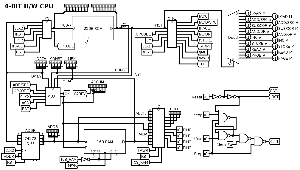
The ALU:

And control:
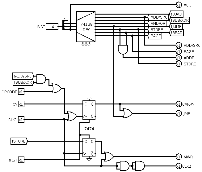
AlanX
Subtraction
I have had a bit of a problem getting my head around subtraction and the borrow/carry flag. With some CPUs (such as the 6502) the carry flag is set and when underflow occurs then the carry flag is cleared. This works of course but makes JNC is not so useful.
The 8086 works the other way. The carry flag is cleared and when underflow occurs the the carry flag is set. Since the 8085 and 8086 were my first microprocessors, I will go with this system, and JNC works better here.
For the time being I am going to "jumper out" ADC and SBB, for ADD and SUB, as these instructions are more trouble then they are worth, at the moment.
I have used the most significant bit of the page register as an OPCODE flag.
Here is the top level view:
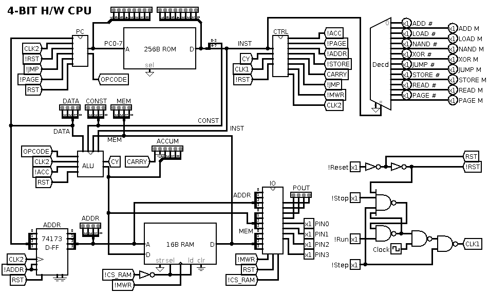
Here is the PC:

And the ALU:
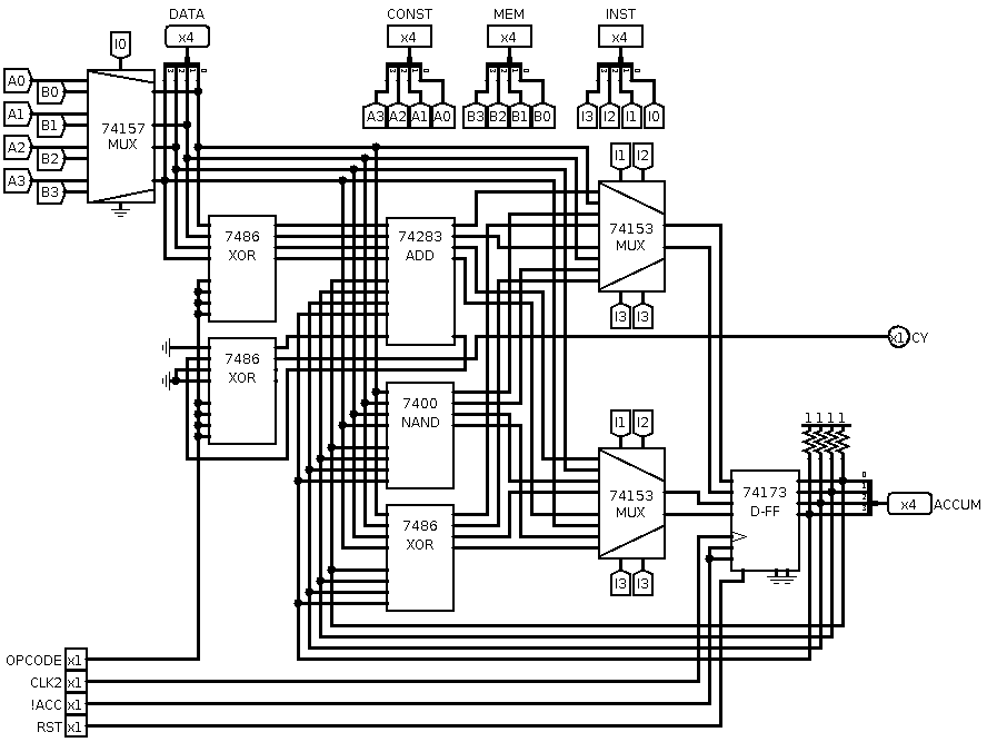
The PAGE op code E0 sets ADD and op code E8 set SUB.
Note E0 00 clears carry while E8 00 sets carry.
It is clear we can add other instructions to the ALU if desired.
Here is some code to count up and then count down. JNC is tripped on overflow/underflow:
E0    Set ADD
00    Clear Carry
20    Clear ACC
AF    Output ACC
A0    Store to Mem[0]
01    ADD 1
83    JNC 3
00    Clear Carry
E8    Set SUB
2F    Set ACC to F
AF    Output ACC
A0    Store to Mem[0]
01    SUB 1
8A    JNC A
E0    Set ADD
00    Clear Carry
82    JMP 2
AlanX
Jump Logic
The current jump logic uses JNC (Jump on Not Carry). It is a complete system but not that intuitive. For multi-nimble/byte arithmetic it is straight forward, if no carry adjustment is required (i.e. not carry), skip the add carry code.
A JGE (i.e. Jump on Greater or Equal) can be constructed by complementing one of the operands, and adding the other operand. Following is an example of testing the input for a program number 1 to 6:
Address    OpCode    Const    Comment    CODE
#    READ PORT
0    C    F    READ F
1    3    F    LOAD M (PORT)
2    0    0    CLEAR CARRY
#    TEST PROGRAM 6
3    0    A    ADD 10         # NOT 5
4    8    7    JNC 7          # JGE 5
5    E    7    SET PAGE       # JUMP PROGRAM 6
6    8    0    JMP ADDR
#    TEST PROGRAM 5
7    0    1    ADD 1          # NOT 4
8    8    B    JNC B          # JGE 4
9    E    6    SET PAGE       # JUMP PROGRAM 5
A    8    0    JMP ADDR
#    TEST PROGRAM 4
B    0    1    ADD 1          # NOT 3
C    8    F    JNC F          # JGE 3
D    E    5    SET PAGE       # JUMP PROGRAM 4
E    8    0    JMP ADDR
#    SET NEW PAGE 1
F    E    1    PAGE 1
#     TEST PROGRAM 3
10    0    1    ADD 1         # NOT 2
11    8    4    JNC 4         # JGE 2
12    E    4    SET PAGE      # JUMP PROGRAM 3
13    8    0    JMP ADDR
#     TEST PROGRAM 2
14    0    1    ADD 1         # NOT 1
15    8    8    JNC 8         # JGE 1
16    E    3    SET PAGE      # JUMP PROGRAM 2
17    8    0    JMP ADDR
#     TEST PROGRAM 1
18    0    1    ADD 1         # NOT 0
19    8    C    JNC C         # JGE 0
1A    E    2    PAGE 2        # JUMP PROGRAM 1
1B    8    0    ADDR 0
#     RETURN - NO PROGRAM SELECTED
1C    E    0    SET PAGE 0
1D    8    0    JMP ADDR 0
1E    0    0    NOP
1F    0    0    NOP
One option is to add a comparator to the ALU and to use one of the flags (i.e. A<B, A=B and A>B) or the compliment to trigger the jump. It would have the advantage of not altering the accummulator.
---
I have been thinking more about this. It would be an efficient and useful to have a "TEST" register but it requires freeing up an op code. XOR being the one to use:
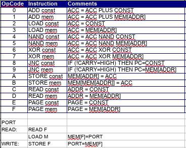
But rather than doing that I am thinking of an op code to select an alternate op code set.
PAGE and READ are similar so they could share the same op code, and the PAGE slot used to set alternate op codes:
Another option is to use the most significant bit of the PAGE register.
ADC/SBB, the ADC requires an inverter on the input and on the output for SBB (have to check this). Does JNC become JNB which is JGE? No need for a dedicated comparator?
AlanX
Add with Carry
To date I have used plain and simple ADD with my DIY CPUs. ADC (i.e. add with carry) is useful for multi byte (nibble) addition as the carry is automatic. The downside is that the humble counter does not work, it skips 0. This can be fixed of course.
Here is the old counter using ADD:
20    LOAD 0          ; CLEAR ACC
A0    STORE MEM[0]    ; SAVE TO MEM[0]
AF    STORE MEM[F]    ; OUTPUT
01    ADD 1           ; INCREMENT ACC
82    JNC 2           ; JUMP ON NOT CARRY
00    ADD 0           ; CLEAR CARRY
82    JNC 2           ; JUMP UNCONDITIONALLY 2
On on overflow you need to clear the carry so that the next JNC is an unconditional jump.
Here is the new counter using ADC:
00    ADC 0           ; CLEAR CARRY
20    LOAD 0          ; CLEAR ACC
A0    STORE MEM[0]    ; SAVE TO MEM[0]
AF    STORE MEM[F]    ; OUTPUT
01    ADC 1           ; INCREMENT ACC
82    JNC 3           ; REPEAT
00    ADC 0           ; CLEAR CARRY
82    JNC 2           ; JUMP UNCONDITIONAL 2
So on overflow you need to both clear the carry and clear the accumulator.
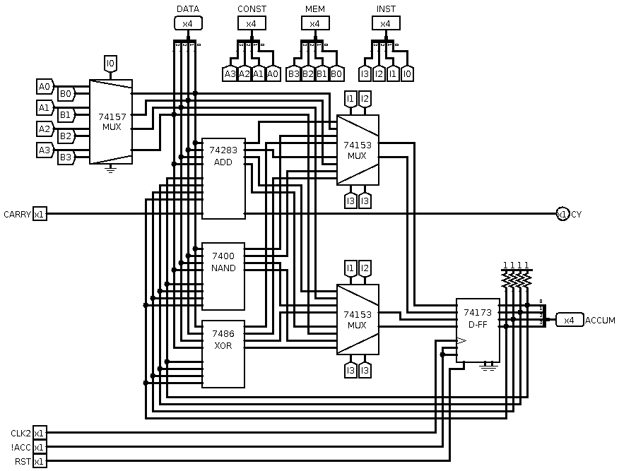
Converting the ALU from ADD to ADC involves linking the Carry signal from the Control unit to the Carry In on the Adder in the ALU unit:
For completeness here is the Control unit:
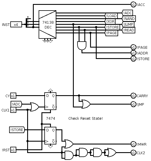
The carry logic holds the carry (CY) until the next ADC instruction.
Multi-Nimble Arithmetic
Before moving on I tested an 8 bit counter using ADC:
00  ADC 0     ; CLEAR CARRY
20  LOAD 0    ; CLEAR ACC
A0  STORE 0   ; CLEAR MEM[0] // LOW NIMBLE
A1  STORE 1   ; CLEAR MEM[1] // HIGH NIMBLE
AF  STORE F   ; CLEAR OUTPUT // LOW NIMBLE
LOOP:
  C0  READ 0  ; PRESET ADDR TO MEM[0]
  30  LOAD 0  ; LOAD LOW NIMBLE
  01  ADC 1   ; INCR LOW NIMBLE
  A0  STORE 0 ; SAVE LOW NIMBLE
  AF  STORE F ; OUTPUT LOW NIMBLE
  C1  READ 1  ; PRESET ADDR TO MEM[1]
  31  LOAD 1  ; LOAD HIGH NIMBLE
  00  ADC 0   ; ADD CARRY TO HIGH NIMBLE
  A1  STORE 1 ; SAVE HIGH NIMBLE
JUMP LOOP:
00 ADC 0      ; CLEAR CARRY
85 JNC 5      ; UNCONDITIONAL JUMP
The ADC does not specifically need the JNC instruction.
The above code is 16 bytes long. A pretty strong justification for a 32 (or more) byte PROM system.
AlanX
Reverting Back to H/W CPU V1
H/W CPU V1 has the paged Program Counter (PC) and most of the control hardware of H/W CPU V2/V3, I just have to delete the ALU tristate buffer, and edit the memory model.
I will call this version V4:
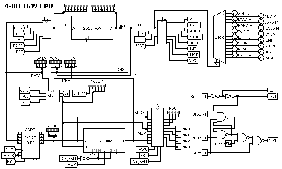
If you want to see meaningless "computer lights" flashing, here is the LogiSim animation:

The code been run is slightly more complicated than the minimum just to check some other instructions:
20    LOAD  0            ; Clear ACC
AF    Store MEM[F]       ; Output ACC
01    ADD   1            ; ACC<=ACC+1
A0    STORE MEM[0]       ; MEM[0]<=ACC
C0    READ  0            ; ADDR<=0, preset memory fetch address
3X    LOAD  MEM[ADDR]    ; ACC<=MEM[ADDR]
AF    STORE MEM[F]       ; Output ACC
82    JNC   X2           ; Jump if no carry
00    ADD   0            ; Clear carry
81    JNC   X1           ; Unconditional jump
The op codes are:

Missing Op Codes?
You may think I am missing op codes such as SHR etc. But no, ADD and NAND are all you need. The rest can be synthesized from ADD and NAND. XOR is included because it needs 14 instructions to read from memory two operands, and to write to memory the resultant. XOR needs 5 instructions to do the same task.
Still, XOR could be swapped out for another instruction.
AlanX
32 Byte Diode PROM
I felt that a 16 byte diode PROM was too small. You cannot fit a program with a subroutine in 16 bytes. So I designed a 32 byte diode PROM, but unfortunately I could not get the auto-router to work. SO the answer is two 16 byte daughter boards:

Here is the schematic:

One nice thing is that the boards are stackable.
I will have to put back the page circuity on the mother board.
---
I have sent the PCB off for fabrication. Usually takes 5 or 6 days.
---
I have made a mistake with regard to stacking the boards. You cannot get 20 pin long headers, typically they are 10 pin headers, and you need a gap between them. Oh well!
I designed a PCB for the 10 long pin headers:

But I am not getting them made until I use up the previous design.
AlanX
Create an account to leave a comment. Already have an account? Log In.
In many respects I am rediscovering the past.
This particular project has been the most fun for me.
LogiSim is a great tool, I don't know how I got along without it previously.
---
I have had thoughts of designing a serial CPU, using shift registers for RAM.
I have some success designing the Accumulator/Adder, but the serial RAM eludes me at the moment. My designs seem more complex than they need to be.
---
The diode PROM boards arrived today. So when I feel energetic, I will solder the nearly 400 components for two 16 bit PROM boards need.
Regards AlanX
I designed the HP1000 A600 minicomputer CPU. The 1000 series never had a subtract instruction! It was always complement and add.
Become a member to follow this project and never miss any updates
 agp.cooper
 kaimac
 zpekic
I am impressed with your project. can you tell me if I can use this for my
https://www.fitnessrap.com/product/helimix-2-0-vortex-blender-shaker-bottle/