-
Ridiculous delvings
01/25/2017 at 23:03 • 2 commentsThe 8087 performs about 50,000 FLOPS
AVRs perform about 60,000 FLOPS (here, and here, and maybe here), definitely on the same order...
I had no idea AVRs could do so many... and here I've been avoiding floating-point in darn-near every AVR project for over a decade. Guess that explains how grbl gets away with it.
------------
In my 1988 edition of Upgrading And Repairing PCs, there's an entire section on "In Circuit Emulators", which, in relation to the PC/XT, were, essentially, 286 or 386 processor upgrades for the 8088-based motherboards. (Like this one)
I dunno why they call 'em emulators... seems like a glorified processor upgrade, to me... But ok.
The section has some interesting commentaries maybe relevant to the current status of this project...
Specifically, mention of "Asynchronous" vs. "Synchronous" ICEs. It says something like an async ICE running at 12MHz is equivalent to a synchronous unit running at 7.2MHz.
Hmmm... Maybe I've put too much effort into trying to synchronize this stuff...? (Are we talking synchronization to the system-bus?). Maybe it'd've worked if I hadn't.
--------
What I don't get, though... Is how these things can speed up a system as much as the author claims... 900%!
It really seems to me like the tremendous bottleneck is the bus... These things don't speed that up... (and remember that *everything* is connected through the bus). E.G. At 4.77MHz, and 4 cycles per transaction (minimum), that's only slightly faster than 1MB/s. Considering an average instruction is two bytes, that's a maximum of 500KIPS, which is right on the order of claims. Throw in some wait-states, the low speeds of DRAMs, the fact that some instructions are as many as 6 bytes, etc... and it's understandable that might drop down to the 350KIPS or less listed. (Remember that the 8088 processor processes instructions *separately* from fetching them, almost as though there are two separate parallel processors internally).
So, *some* of these "in circuit emulators" have a full 640K of onboard RAM (some even more), so plausibly there's a faster bus onboard, and the 8088 motherboard is basically little more than some ISA slots and a few peripherals. At which point, the ICE is basically an entire 386 motherboard (daughter-card?) that happens to plug into a "backplane" via a 40pin DIP socket.
But, surely, it still has to make use of the original DMA controller, etc... huh. So, at some point, the "emulator" must keep track of where its bus-transactions should be directed, and prevent them from going to the 8088-bus if they're actually happening onboard (e.g. onboard RAM). Weird stuff. Guess it is a bit more than just a processor upgrade. Wonder if it has to "boot" first, or whether those sorts of things are handled by logic-gates.
And, what if there's an 8087 on the motherboard...? Does the ICE just "lie" by indicating idle-states, to essentially deselect it during all transactions? Guess that's where "emulation" comes into play.... hmmm. Oh, I suppose that'd be similar to a DMA, which wouldn't indicate Queue-Statii during transactions... so the 8087 (any others?) just wouldn't pay attention... Ah Hah.
Actually, that all seems quite similar to what I'm attempting... just that my attempts are much slower ;)
-
AVR Clocking (overthinking)
01/24/2017 at 21:44 • 0 commentsA nice surprise, that I'll save for future-endeavors:
![]()
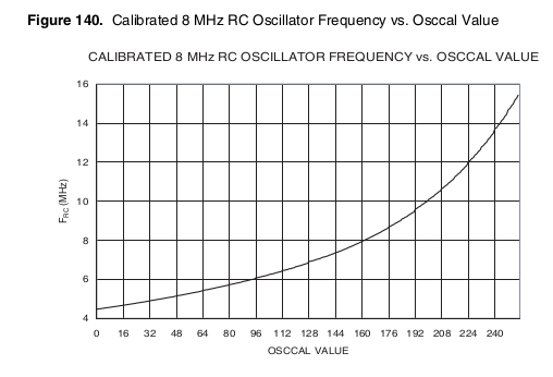
I figured OSCCAL would allow adjustment of the 8MHz (nominal) R/C oscillator with only a small variance in either direction, but here it seems I could adjust it to (roughly) Three Times the 8088 Bus Clock (14.31MHz)!
I've vague ideas of how to fine-tune that... maybe using an 8-bit timer/counter, and counting external 4.77MHz clocks until it overflows, counting internal clocks at the same time, and adjusting the OSCCAL value until we get ~768 internal clocks between timer-interrupts. That'd probably be accurate-enough... Especially if I have a routine that waits until an edge is detected before starting each bus-transaction.
It's entirely plausible it'll sync-up somewhere mid-clock, and that's something I'll be pondering. Maybe it means we can only, reliably, execute two timing-sensitive instructions per bus-clock... I dunno.
---------------
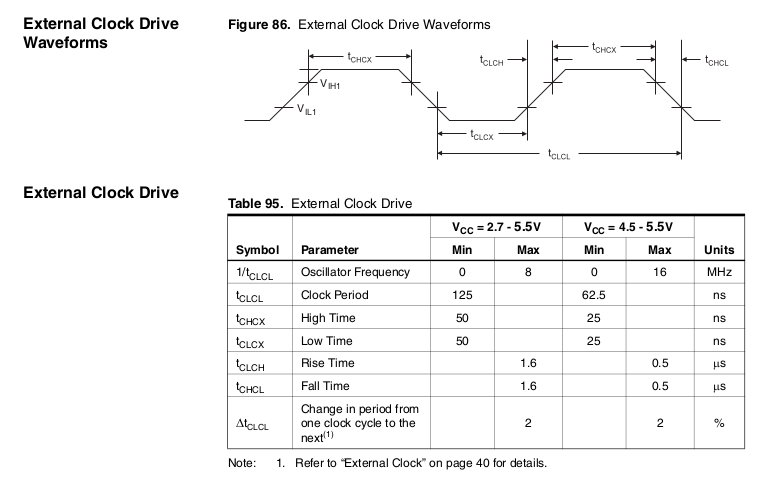
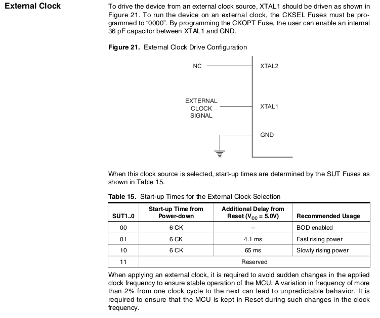
External-clocking at 4.77MHz (1:1 AVR/8088 clocking) also seems feasible (and would certainly be easiest for these early experiments):
![]()
Note, no mention of duty-cycle. (and, in fact, the drawing isn't even close to 50%!)
![]()
(because, the 8088's clock is 4.77MHz with 33% duty-cycle).
-------------
Finally: I think I've managed to whittle down the bus-transaction such that with 1:1 clocking, the AVR should be able to keep up within the requirements of external memories and I/O (and the 8288). (Though, NOT, the 8087 and DMA controller... which I'll leave uninitialized for now).
#define S20_INT_ACK     0x0
#define S20_READ_IO     0x1
#define S20_WRITE_IO    0x2
#define S20_HALT        0x3
#define S20_INSN_FETCH  0x4
#define S20_READ_MEM    0x5
#define S20_WRITE_MEM   0x6
#define S20_PASSIVE     0x7
#define S20_IDLE    S20_PASSIVE //my own naming...

void bus88_write(uint8_t s20, uint32_t address, uint8_t data)
{
   //////
   // 4.77MHz = 209.6ns
   //  clock-high = 33% duty-cycle = 69.88ns
   //  clock-low =  66%            = 139.76ns

   //////
   //AVR latches inputs on the falling-edge
   // 'in R17, PINA' is valid *half* a period after, or in the *next*
   // clock-cycle
   // (and R17 contains the value at the rising edge of the one following)
   //
   //AVR latches *outputs* on the rising-edge *after* the instruction
   // completes.

   //Note, all AVR-OUTPUTs, here,  are expected within ~20ns after bus's
   //       Falling-edge
   //      all AVR-INPUTs, here, are expected within ~20ns after bus's
   //       Rising-edge

   // So, maybe a 7404, or something, could be found with ~20ns
   //  propagation-delay, and wired between the bus-clock and the AVR
   //  clock-input.
   //  Or, chain a few inverters in series.
   //  (Believe it or not, this was once a go-to method for synchronizing
   //   digital logic... Sometimes you'll even find a production-board with
   //   a chain of inverters and a clock-signal hand-wired to a point
   //   somewhere inbetween)

 //### Bus is idle (assumed) ###

   //So, it should be OK to prep our Address bytes
   ADDR1916_PORT   = (uint8_t)(address>>16); //assuming bits 20-24 are 0
   ADDR158_PORT    = (uint8_t)(address>>8);
   ADDRDATA70_PORT = (uint8_t)(address);

   //Begin the Bus transaction
   //Per 8288:
   // This should happen between tCHSV after _|¯ and tSVCH before next
   // tCHSV = Status Active Hold Time >= 10ns after _|¯
   // tSVCH = Status Active Setup Time >= 35ns before next(?!) _|¯
   // So, basically, somewhere around T1's entry ¯|_
   S20_PORT       = s20;   // OUTPUT, AROUND: ¯|_

   // The 8288 will bring ALE High...
   //  Either from the clock ¯|_, or from S20 ¯|_, if after clock

 // ¯|_  ### T1 ###
   // Normally, Addresses would be setup here,
   //  but we're fudging the timings a bit...
   //  They've already been done.
   // The 8288 will bring ALE Low in 4-15ns after _|¯

   //Nothing to do?!
   // Gotta keep the timing aligned...
   asm("nop;");

 // ¯|_  ### T2 ###
   // "T2 is used primarily for changing the direction of the bus during
   //  read operations" -- 8088-CPU.pdf
   // The 8288 will bring /AMWC, /AIOWC, etc. low in 10-35ns after ¯|_
   //  for "advanced" (early) write-signals
   //  (Not really important to note here)
   // FOR READ: This is the same time where /MRDC, or /IORC occurs
   //TODO: Should probably make sure the ALE pulse is recognized
   //  by other devices, before we change AD7:0
   //  BUT: it's already been half a clock-period, right?
   //  So should be fine...
   //  ALSO, if we meet/exceed the 8088's minimum timings, here,
   //  then it should be fine.

   //Put the data-to-write on the port
   //8088: TCLAX ¯|_ -> A19:16 -> S6:3 Address Hold >= 10ns
   //      TCLAZ ¯|_ -> AD7:0 -> Float (READ) Address Float Delay 10-80ns
   //      TCLDV ¯|_ -> AD7:0 -> Data (WRITE) Address Valid Delay 10-110ns
   ADDRDATA70_PORT = data;  //OUTPUT: >10ns AFTER ¯|_


   //Technically: A19:16 -> S6:3 is also supposed to happen here
   // but for now we're not using the 8087, nor DMA, so should be OK(?)

 // ¯|_  ### T3 / Tw ###
   // The 8288 will bring /MWC, /IOWC, etc. low in 10-35ns after ¯|_
   //  for *non*-advanced/non-early write-signals

   //It's not possible to read the READY signal, test it, then jump
   // all in a single AVR cycle
   //Thankfully, it seems the 8288 is triggered only by /S2:0
   // And the processor is the only thing that pays attention to READY
   // And, nothing else is expected of the processor outputs during T3/Tw
   //So, we can insert our own "wait-states"
   // in the form of internal processing-time, then return /S2:0 to "idle"
   // when it's complete

   //According to one diagram (showing READY being sampled!)
   // READY should be sampled with ¯|_ entering T3/Tw
   // in 8088-CPU.pdf p10
   //According to another diagram, READY should be sampled with _|¯
   //!!! TRYLCL could be up to 8ns *into* T3 (but not Tw)
   // TRYHCH setup time > 118ns to _|¯ mid T3/Tw!!!
   // TCHRYX hold-time > 30ns after _|¯
   // in 8088-CPU.pdf p23
   //Confusing, but the actual *timings* suggest _|¯
   //
   // OK, sample READY on _|¯
   while(!(READY_PIN & READY_MASK))  {};  //INPUT: <30ns AFTER _|¯

   //NOTE That we'll be in a later Tw, at this point... weeee!
   //Indicate that we're done with wait-states, and ready to enter T4
   //8088: TCLSH Status Inactive Delay: after ¯|_ 10-130ns
   S20_PORT = S20_IDLE; //OUTPUT: >10ns AFTER ¯|_

 // ¯|_  ### T4 ###
   // The 8288 will bring /IOR, /IOW, etc. high within 10-35ns of ¯|_
   // We're not reading, so we don't need to sample ADDRDATA_PIN
   //  But, for READ, it should be done quickly after ¯|_, or maybe before
   // 8288 timing shows Write Data Valid as acceptably valid after T4
   //  Same likely goes for A19:8... (whew!)

   //Nothing to do?!
   asm("nop;");

 // ¯|_  ### BUS IDLE ###
   // WARNING: This is NOT compatible with DMA and 8087!
}
In case you didn't catch that, lemme take out the majority of the comments:
   ADDR1916_PORT   = (uint8_t)(address>>16); //assuming bits 20-24 are 0
   ADDR158_PORT    = (uint8_t)(address>>8);
   ADDRDATA70_PORT = (uint8_t)(address);

   S20_PORT       = s20;   // OUTPUT, AROUND: ¯|_

   asm("nop;");

   ADDRDATA70_PORT = data;  //OUTPUT: >10ns AFTER ¯|_

   while(!(READY_PIN & READY_MASK))  {};  //INPUT: <30ns AFTER _|¯

   S20_PORT = S20_IDLE; //OUTPUT: >10ns AFTER ¯|_

   asm("nop;");
SO MUCH SIMPLER than the earlier expectations, wherein I thought it would be darn-near impossible to get it running with a 4:1 AVR clock. And, here it should work with 1:1.
------------
I've still gotta wire this thing up, and the cat's being deprived, so it may be a while until I get a chance to check this out.
Thankfully, READ is pretty much identical, (and has been accounted-for in the comments)...
And it'd be pretty easy to e.g. use the AVR's UART (or just an LED) to indicate whether writes/reads to a low memory-address verify correctly. (A bit of a shout-out to comments in earlier logs, suggesting using the AVR's peripherals... I'd been planning to do some CGA video-output for my first "hello-world" but that's way overboard)
--------
And... the 8515 might just work with only a few pin-relocations, it's got a very similar pinout to the 8088.
-
Bus Timing Simplified again again?
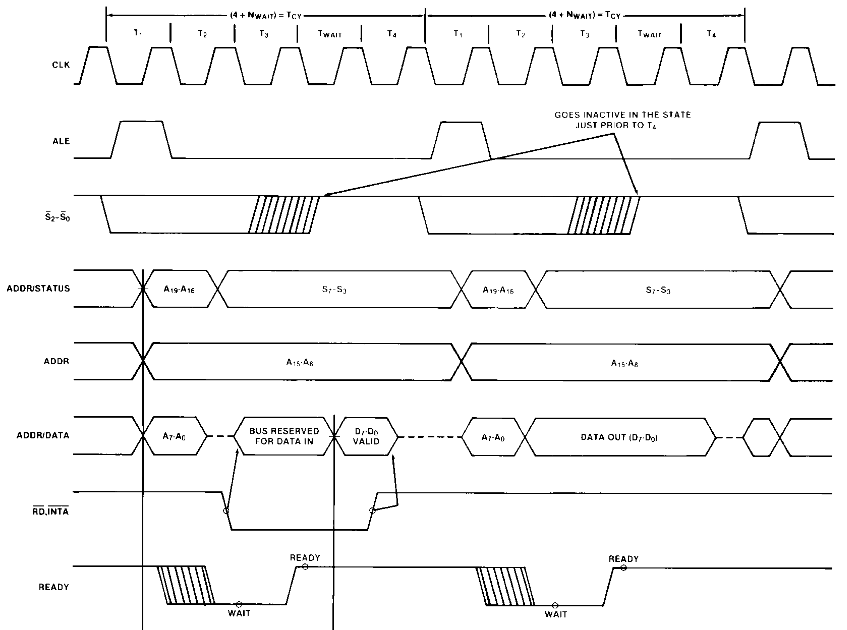
01/24/2017 at 11:24 • 0 commentsAh HAH! The 8288 doesn't *need* the "READY" signal... it bases its actions on the /S2:0 signals, sent by the CPU.
(This may sound obvious to you, but I spent *numerous* hours tracking down signals in schematics before coming to that conclusion.)
If I understand correctly... this may be a *tremendous* advantage...
![]()
Again, the CPU is responsible for responding to the READY signal input. And it does-so by basically delaying everything until READY is true... and it goes about delaying the *bus* by keeping /S2:0 in their current state.
This, again with the SRAM example, is the equivalent of keeping the /RD or /WR signal active for an extended amount of time. That's no problem.
So, let's say it takes three instructions to read a READY signal, and jump back to the ready-test if it's not ready... And, say that's running at the bus-clock... so, technically, it would take three bus-clocks just to process the READY signal. That's *in no way* within the specs of the 8088, which can handle it within a single bus-clock. BUT, it shouldn't matter, right?
So, if the device is ready, immediately, we'll waste 3 bus-cycles reading that in, and breaking from the loop... The effect, then, is just that the CPU itself added 3 wait-states of its own. (Which isn't spec'd anywhere, but, now, seems like it should work).
If the device is *not* ready, immediately, then we'll only be able to test it once every three bus-clocks... Oh well.
So... I think the ready thing is resolved.
(Note that all this relies on the fact that I'm *not* using an 8087 FPU, nor the DMA controller, or other things that might try to take over the bus).
----------------
Here's a more programmatic view of the timing-diagrams...
Modified a bit for an AVR... but not yet including my READY-processing with a 1:1 AVR:Bus clock-ratio.
## IDLE ##
   A19:16
   A15:8
   A7:0
   S2:0 //Begin transaction
## T1 ##
    (8288: ALE Low, immediately before T2)
## T2 ##
    (8288: /WR low (WRITE))
    *right before CLK^*
     A7:0 -> Input (READ) / D7:0 (WRITE)
   (CLK ^)
    A19:16 -> S6:3
     (8288: /RD low (READ))
## T3/Tw ##
    --SAMPLE READY/!WAIT
     (READ: "Bus Reserved for data in")
    IF READY (FALSE, for this example)
      S2:0 = IDLE
      (CLK ^)
      (8288: /WR high (WRITE))
    ELSE
      Repeat T3, call it Tw
## T4 ##
    --SAMPLE (READ)
    (8288: /RD high (READ))
    D7:0 -> float (WRITE) (PROBABLY only need for bus-masters, DMA, etc.)
   (CLK ^)
## IDLE ##
So, now, I think the only thing remaining to be figured out is how to handle T2 which has two instructions: Modifying AD7:0, and outputting S6:3.
(Oh, and I've been ignoring the /QS bits, I think those are only required when using an FPU. The same might be true for S6:3...?)
-------
Hahahaha! Ridiculous!
The "bus masters" such as the DMA controller, interface... *with the bus*... I dunno why I didn't think of looking at them, instead of the 8088/8288.
And, yahknow, I don't think they implement things like /S6:3, etc.
-
Bus-Timing simplified again
01/23/2017 at 16:43 • 0 commentsIf you've read the last logs, you'll know I've been caught-up in trying to meet the 8088's bus-timing, using an AVR.
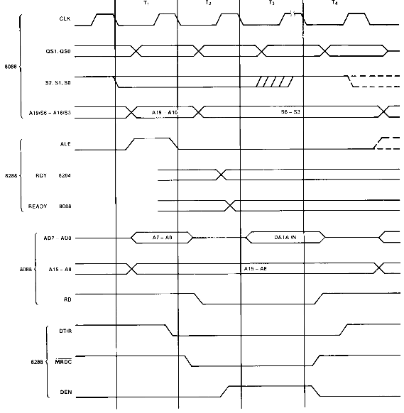
![]()
I think I went way overboard.
In one of the later logs on the matter I realized: It's not that I need to meet the 8088's *output* timing-specs, but that I need to meet the *input* timing-specs of the devices attached to it.
That certainly lowered the requirements on my AVR, but I still visualized a lot to be done within specific timings... Including (and probably most-difficult) setting up 20 address-bits, the S2:0 signals, and the QS1:0 signals, all within a single bus-cycle (at 4.77MHz). 25 bits to setup within one bus-cycle would, if set-up prior to the bus-cycle, require my AVR to be running 4x faster than the bus (writing one byte at a time).
Maybe, prior to that bus-cycle, I could've set up a timer output to toggle one pin within that cycle. Thus, not requiring an explicit instruction to be executed within that cycle to change that pin within that cycle... that'd bring the bit-count down to 24, three bytes would still require the AVR to be running at least 3x faster than the bus.
-----------
Tonight an epiphany.
If the bus is *idle* then it shouldn't matter what happens on the majority of the signals.
In other words: imagine an SRAM whose Chip-Select is disabled... It doesn't care what happens on the address lines.
Similarly, even if Chip-Select is enabled, changing the address lines willy-nilly doesn't affect the functionality of the SRAM until /RD or /WR is activated...
So, for all the SRAM ('device') cares, I could've set-up the address lines *hours* before-hand, if I wanted to.
The same could, likely, be said for most (maybe all) chips connected to the 8088's bus.
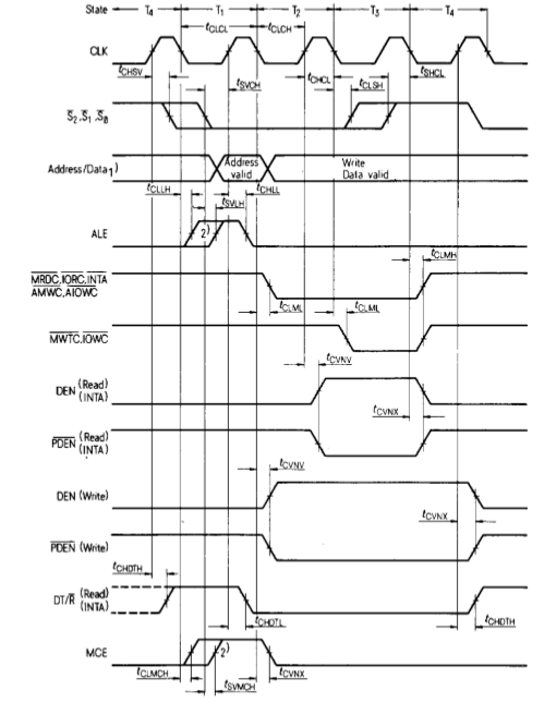
Right now I'm looking at the 8288, which, essentially, converts the 8088's multiplexed /S0-/S2 signals into various /RD and /WR signals...
![]()
Basically, the vast-majority of 'devices'--be they on the ISA slots or on the mother-board--only receive their /RD, or /WR signals *through* the 8288. So, for those devices, as long as I meet the 8288's requirements, everything should go smoothly.
And, that's what I was missing, somehow, before...
I haven't looked at all the details, but It looks like /S2:0 basically initiate the transaction... The 8088's timings are such that transactions *could* execute back-to-back. But I don't have to do that (and probably can't) with my AVR...
So, instead, keep the bus "idle"... then set-up the address-signals (20 bits!), and only *then* set up the /S2:0 signals, to indicate that it's ready to transact.
BAM.
Now, it *almost* looks like I could get away with one AVR instruction per bus-cycle. Which would certainly be easier...
because... one of the ongoing other difficulties (mentioned in previous logs) was trying to figure out how to synchronize a faster AVR clock (e.g. 4 * 4.77MHz) with the 4.77MHz clock-input.
Now, it would seem, I could almost use the bus-clock to directly drive my AVR.
----------
So, that'd be easiest, if it works... and everything hereafter may be overkill (though beneficial):
1) There may be a little bit of difficulty running at the same clock: the bus-clock has a 33% duty-cycle. I haven't located requirements for the AVR's external-clock input, but I vaguely remember having read that it's supposed to be ~50%... I have located a portion in the datasheet specifying that the clock shouldn't vary more than 2% from cycle-to-cycle... Not sure how that's relevant.
2) When reading, address-data must be output to the associated port during one bus-cycle, then the port needs to be turned into an input, then a port-read needs to occur... Can all this be accomplished with appropriate timing? (Note that the PIN register is *delayed* through a latch, so the actual variable=PINx; instruction would have to occur one(?) AVR clock-cycle *after* the bus-clock edge where it's expected... Maybe that'll be helpful.
3) None of these diagrams show the READY signal, which can be used by a device to indicate that it's not yet ready, thus delaying everything for additional bus-cycles. (Interestingly, I don't see where that signal goes into the 8288, so how does that work?!) If the AVR has to test a pin (READY) and react, we're talking about a read, a comparison, and a jump... at least three instructions... Hmmm...
4) Maybe rather than using the bus-clock to drive the AVR directly, it could be used with a timer-input pin and upon boot the AVR will synchronize its internal R/C clock to the external bus-clock via OSCCAL. I'm totally guessing, here, but it's rated for 8MHz nominal, so maybe 2 * 4.77 is possible. (Doable with an AVR that doesn't have a PLL, which is a plus, since my PLL-AVRs have too few pins... and a workaround discussed in a previous log).
5) Technically, I suppose, it doesn't *have* to be perfectly-synchronized, most operations aren't expected to happen *at* an edge, but some specified time *before* one... so "dead-reconning" may be possible, with some rough-estimate of how many AVR clocks fit in a bus-transaction (4+ bus-clocks), and some synchronization at the beginning of each transaction.
-
We Have A BIOS Extension!
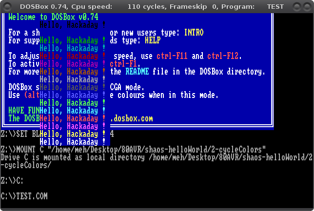
01/15/2017 at 21:00 • 32 commentsUPDATE: Adding screenshot from 'dosbox'
------------
Thanks to @Shaos's hard work getting a PCjr ROM-Cartridge working over at #PCjrCart (https://hackaday.io/project/19160-pcjrcart/log/51792-creating-a-bios-extension), my work getting my first ROM extension was greatly reduced!
Here it is running as a .COM under 'dosbox'
![]()
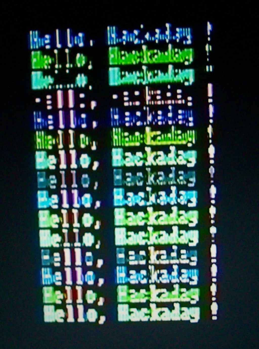
And here it is as a ROM-Extension on my PC/XT clone:
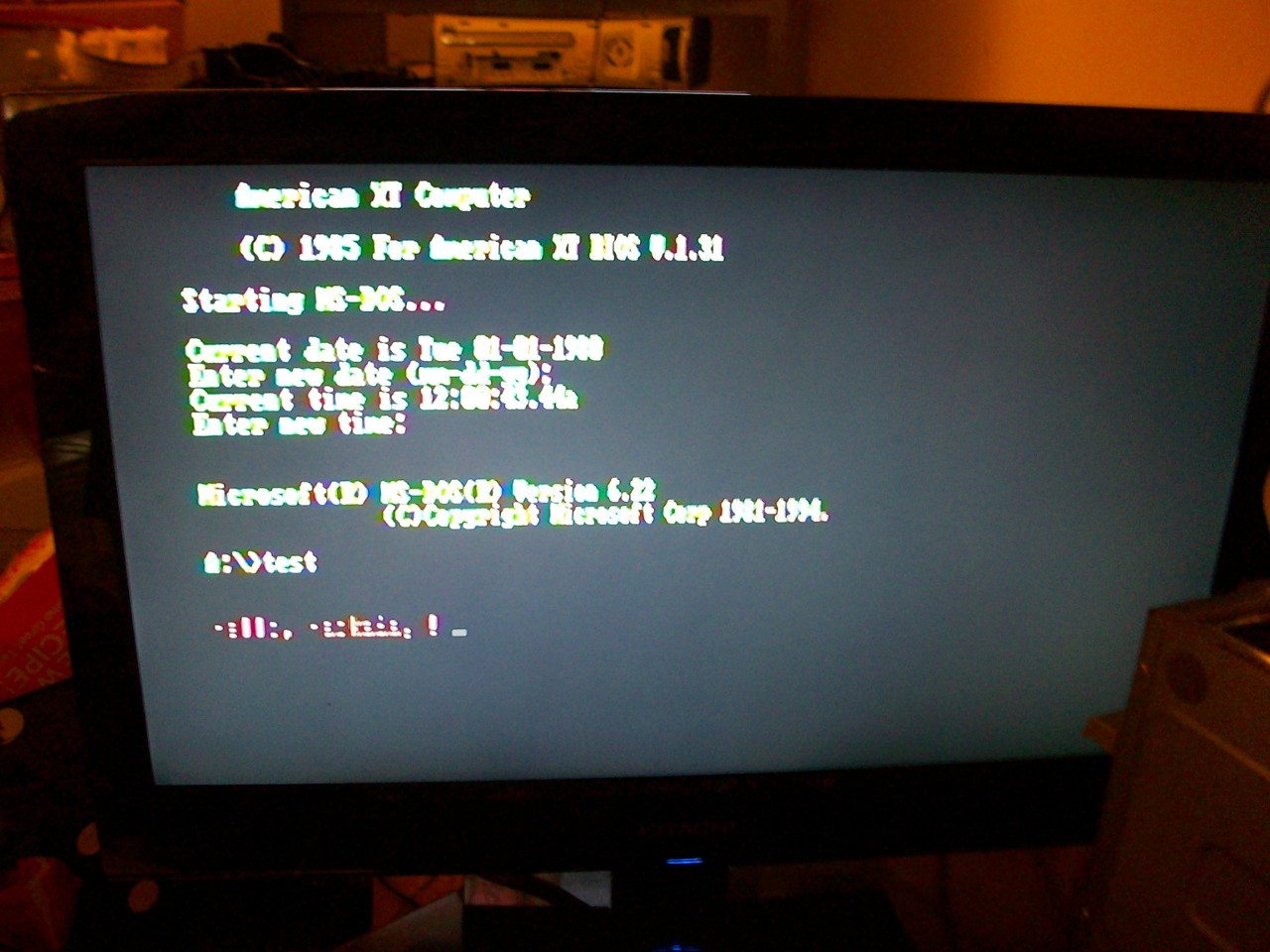
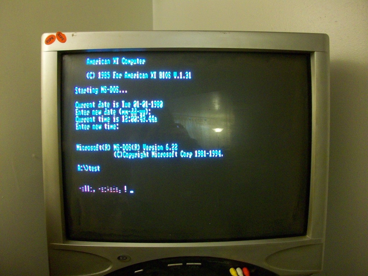
Apparently on the XT, it runs the BIOS extensions almost immediately in the boot process, so this is on a completely black background. (Note that it cycles through text-colors as well as background-colors).
And I learned a lot, along the way.We've got the BIOS in the ZIF socket on the left, because that's where I intend to do most of my work, later down the road... (and I found another BIOS to try out floating in the 'old chips' box).
And we've got the "BIOS-Extension ROM" further to the right.
A couple notes:
- It Boots FAST (no memory-test beforehand?!)
- The PC/XT apparently doesn't start in the same video-page as the PCjr, so a simple fix is to use INT10H to read the current page, then reuse that value instead of hard-coding it. Sum total of 1 additional instruction, and one modified.
- The PC/XT doesn't use a CRC to validate the ROM-extension, instead it uses a simple checksum (8-bit). My quick-solution: hand-edit the binary, replacing the last two bytes with 00 and the checksum
- My PC/XT's video arrangement is pretty wonky (which you probably guessed if you've read my last logs), so the original choice of RED for the text resulted in basically "_| -| || -_ |-" which is why I've modified his code to cycle through the foreground and background colors to find a decent choice (of which there are few).
Here's the first-experiments. Before loading it into a ROM, you can try out the .COM executable under DOS...
-------------------
I won't give it *all* away... but go grab @Shaos's code from github (again https://hackaday.io/project/19160-pcjrcart/log/51792-creating-a-bios-extension)
Make sure you've got 'nasm' installed (the Assembler)... Look up "INT 10H" (wikipedia's got it)
You might want to install 'dosbox' as well... when running it slow the "cycles" to ~300 to mimic a PC/XT's execution-speed.
Here's a makefile to make things easier...
default: gcc -o pcjrcart pcjrcart.c crc16.c nasm test.asm -fbin -o test.com ./pcjrcart test.com clean: rm -f pcjrcart test.com test.bin run: dosbox -machine cga test.com -
shoulda known better...
01/14/2017 at 10:19 • 0 comments...than to click on a youtube video in the midst of having-written for well over an hour, without Lazarus(?) installed... :/
Whelp, suffice to say, I'm trying out @Shaos's instructions, here: https://hackaday.io/project/19160-pcjrcart/log/51792-creating-a-bios-extension/discussion-74094 and made some modifications to make it XT-compatible (test the current page, rather than assuming page 7). And some more modifications because my stupid video-setup doesn't show anything other than "|-_|| -| |_" when displayed in red, or most any color, for that matter.
Anyways, a great starting-point.
I wasn't planning on doing BIOS extensions, as the whole point (at this point) in the project, of doing a custom ROM, is to limit the number of executed-instructions to those I've actually (at that time, when I get there) implemented... Which, wouldn't at all be limited by the BIOS, itself, which is run before the BIOS extensions...
BUT: his work, there, is a *GREAT* starting-point... showing how to use nasm, and more...
And, I think, PCjr cartridges basically work *identically* to PC/XT bios-extensions. And some ideas 'round that link, regarding how to use those bios-extension/PCjr-cartridge memory-locations as Read/Write, despite not having a /WE pin... in which case you can throw custom hardware, there, too.
-
state of the cpu address
01/13/2017 at 22:23 • 0 commentsThanks to @jaromir.sukuba for inspiring this writing...
The point of this project is[/was?] to implement the 8088 chip itself, with an AVR... making use of the other peripherals already on the original mother-board, not because they're *better* than the peripherals available in an AVR, but because *nearly everything* is interfaced to the 8088 in the same way, including the "program memory" (BIOS), the RAM, and the I/Os...
There's been discussion--as well as browsings mentioned in past logs--wherein it's suggested to use the AVR's internal peripherals to *replace* those on the motherboard... That'd be smart. In fact, it'd probably be *much* faster if that was done.
E.G. writing a byte from a string stored in the AVR's internal memory into the TX-register in the AVR's serial-port would probably take something like 2 AVR instructions, maybe 4 AVR clock-cycles. On the other hand, doing-so, even without emulating the 8088's instruction-set, to an externally-attached ISA RS-232 card would require, at the very minimum, 4 8088 bus clocks (one 8088 bus cycle).
I think I can somewhat-reasonably expect to execute 5 AVR instructions per every 8088 bus clock... (4.77MHz * 5 = a slightly overclocked AVR). So we're talking a bare-minimum of 20 AVR-clock-cycles to transact a single byte of instruction/memory/I/O data... And that's assuming no wait-states, assuming the Bus-Interface-Unit (BIU) isn't already in the middle of a transaction (e.g. caching the next instruction-byte), that DMA isn't refreshing the DRAM, etc.
That's a *huge* hit, for *every* byte-transaction. And, again, doesn't even consider the fact that the AVR will be emulating the 8088's instruction-set.
Now, again, consider (as @jaromir.sukuba brought up, and was brought up in previous logs) just how much could actually be implemented *within* the AVR... The PC/XT BIOS-ROM is 8KB... Many AVRs could fit that and still have plenty of space for AVR-code. So, the BIOS itself could be stored in the AVR... Reducing the read of each byte from 20AVR cycles to 2-3, during boot, interrupts, and more. The RS-232 port, maybe I2C for a keyboard... (or even bitbanged PS/2!)... Even SPI for an LCD. Could even load a bunch of RAM in there, as well. And all these "devices" would communicate *significantly* faster when directly-interfaced with the AVR-core, rather than going through the 8088-style bus.
Also, consider that the 8088 contains two "units" which run *in parallel*. The Execution Unit (EU) actually executes instructions, but the Bus-Interface Unit (BIU) grabs data from/writes data to the bus. The BIU runs *in parallel* to the EU, so while the EU is executing instructions, the BIU is often fetching the next data-bytes for the next instructions, simultaneously. This could, in a way, be considered like a DMA transaction... Well, 8bit AVRs don't have DMA, especially one that'd be compatible with the 8088's bus-interface. So, that means each transaction on the bus has to be handled by the "CPU", making the entire system more like a lock-stepped single-core system, rather than a dual-threaded, dual-core system that the 8088's EU/BIU more closely approximate.
Similarly, consider an 8088 bus-transaction's being 4 bus-clocks, being 20 AVR clocks, being ~20 AVR instructions... Worst-Case, a bus-transaction transfers something like 6 bytes. We're talking 3 bytes for the address, 1 for data, and numerous control signals. The vast-majority of the signals need to be set-up early-on in the transaction... That means the AVR "core" would be executing numerous instructions as fast as possible to set up those byte-transactions. But, thereafter, the AVR core will just have to twiddle its thumbs waiting for the various bus-clocks, wait-states, and delays, thereafter.
Those bus-clocks, again, come at something like 1 every 5AVR cycles... So, one might think "use interrupts!". Herein we run into some realities... First of all, some (though few) AVR instructions can take as many as 5 clock-cycles. And, interrupt-processing waits until the current instruction is done executing. If those multi-cycle instructions were limited to "extremes" like "MULT", one could say "well, just make sure you don't use MULT while waiting for that next bus-clock". But, unfortunately, some of those instructions are not that unusual. E.G. Reading/Writing the internal SRAM takes several cycles, despite being single instructions. And, in fact, if I recall correctly, AVR's RETI (Return From Interrupt) instruction, alone, takes 5 clock-cycles.
So, using interrupts to handle bus-clocks isn't really possible. Which means the AVR will be busy-as-heck in those early bus-clocks, setting up the address/control signals, and NOPing during the later bus-clocks, NOPing for the majority of the bus-transaction.
Now, I suppose, if one's clever, those NOPs could be used for other purposes, and indeed some might (e.g. somewhere within there, we'd need to *read* the data coming back from the device). But, whatever's done, there's not enough time to handle e.g. waiting until an edge is detected, then jumping once it is, then performing what needs to be done. So, instead, we need to know the ratio of the number of AVR cycles to the number of bus-clocks, and keep track of exactly how many instructions occur between each clock... (and how many AVR cycles those instructions take!) ("dead-reconning" maybe?). Similarly, there's probably not enough time between each clock to run tests, e.g. "am I writing? Then output the data-byte. Otherwise read a data byte". Instead, we'll have to prepare these instructions *prior* to initiating the bus-transaction, And likely some instructions will have to be run regardless of whether the operation calls for it.
E.G. a bus transaction could be either a read or a write... The read case is easy... Just read the port-inputs *every* time, and if we're writing just disregard what was read. The write case is only slightly more difficult. One way to be able to handle *both* within the same bus-transaction function would be...
Before beginning the transaction, prepare our port-configuration variables... if writing, PORTx = Data, and DDRx = ALL_OUTS, if reading PORTx = 0x00 (no pull-ups), and DDRx = ALL_INPUTs. But, again, we can't write those registers willy-nilly, they have to occur within certain bus-clock timing-requirements. So, we can't do
while(!clock-edge) {};
if(read) {
   DDRx=ALL_INS;
   data = PINx;
} else {
  //(DDR's already out)
  PORTx = data;
}
as we've already exceeded our clock-cycle by merely running those if-tests and jumps. Instead, e.g.
//BEFORE beginning a bus transaction:
registerA = (doRead ? ALL_INS : ALL_OUTS);
registerB = (doRead ? DONT_PULL_UP : writeVal);

BeginTransaction...;
<do early bus-transaction stuff>;
DDRx = registerA;
<NOP until the WRITE clock-edge>;
PORTx = registerB;
registerC = PINx;
<do remaining bus-transaction stuff>;
//After transaction is complete:
if(doRead)
  *readData = register c;
(This should be done in assembly. I've explained why elsewhere, but basically, the optimizer is likely to choose to reorganize the code).
...or, yahknow, you could have two separate functions for read vs write transactions (how'd I not see that weeks ago?). However, the above is only a tiny fraction of the entire bus-transaction, most of which is identical in both cases.
Anyways, at some point, if this system is to interact with *real* 8088-compatible hardware (any), then the system has to interact with external peripherals in an 8088-compatible manner... I kinda want to run a soundblaster and CGA card from my AVR... SCSI... Maybe HPIB... Maybe even build some ISA cards of my own. OTOH, maybe interfacing with ISA directly, rather than the 8088-bus, is a better idea. Anyways, the goal of this project isn't to emulate an 8088 system, but to emulate an 8088 *chip* (otherwise, just run dosbox!).
----------------
So, again, instead of the 8088's separate/simultaneous/parallel BIU/EU system, a single AVR simulating the two would have to be more of a state-machine...
A mad rush to request an instruction-byte, then a bunch of NOPs waiting to "Download" it, then decide if we need to request more bytes for our instruction, then execute, then download more. No caching, etc. It'll be a big performance hit that doesn't really have anything to do with the AVR's comparable computing-power, and something that I'm contemplating whether to continue in that way, or whether to take another path.
One obvious idea is two separate AVRs, one for the EU and another for the BIU. I've a lot of thoughts on the matter... Boils down to whether the two systems can communicate fast enough to justify it...
A regular 8088-bus-transaction would take a minimum of 20 AVR clocks per bus-cycle (to read or write a single byte of data). There's something like 6 bytes of transmission (data/address/control-signals) during a bus-cycle... (maybe five by considering that the BIU tracks the segment-registers)... So, you might think there's a significant improvement in speed (6/20ths!) by communicating to the separate BIU-AVR, rather than directly to the bus, itself.
But there's also some time to synchronize the two AVRs, since byte-wide transmissions can't go on in the background... The EU will still have to wait for the BIU to complete its bus transaction (can bus-transactions be interrupted and restarted?). The BIU will have to enable interrupts, or otherwise test, for when the EU has begun an "inter-processor-communication", then send an acknowledge... The EU will most likely be doing nothing but waiting for that "ACK", so will be able to respond, almost immediately, with the burst of 5 remaining data/address/control bytes (at 20+MB/s!).
But with all that ACK/response and waiting, even sending data in parallel I think we're talking something like a minimum of 15-20 cycles per transaction. Nevermind, again, waiting for a previous BIU transaction to complete before it can turn on interrupts, and whatnot... and we're right back where we started... Maybe multiple simultaneous serial I/O's, since the serial peripherals have buffers...? Or, a byte-wide, six-long shift-register setup? That's a lotta 74574's! (And, still doesn't help when *reading*).
Weeee!
----------
So, the suggested "project-scope creep" of using the AVR's internal peripherals/ROM/RAM may be somewhat reasonable for early-experiments in this project... Besides being a faster system, it'd also, likely, be easier to implement. A fully-functional (albeit limited) *system*, running 8088/86 code, could probably be implemented in the AVR without even touching an 8088 bus, nor implementing a BIU. The peripherals themselves would be much easier to interface with, as well, even at the register-level alone (and ignoring the BIU inbetween) (especially since I'm already familiar with so many AVR peripherals).
And, atop all that, if the BIOS (which'd have to be custom at that point, which really doesn't matter because I planned on custom/limited program-code in the first place while implementing instructions a few/one at a time)... if the BIOS was implemented in the AVR, as well, then it would be flash/in-system-programmable, making early experiments *that much easier*.
And, without all those bus-transactions, the entire system might well be "screaming fast", even in comparison with the original 8088 chip running in an XT.
So, it's something to seriously consider...
---------
If I take a step back and think about what led up to this project, I realize the original goals weren't at all about emulating an 8088, but about interfacing with its hardware; using the motherboard, ISA-slots, etc. as a platform, and with a processor I'm familiar with (AVR). So, this project has already "scope-creeped" quite a bit from my original intentions. On the plus-side I've learned a bit about an architecture that was a complete "black-box" to me (x86). This whole emulation-aspect has been a bit of a side-track, but I've learned to read/understand x86 assembly, and I've tangentially learned about the low-level/register-level interfaces of the sorts of devices I'd originally intended to interface with. (e.g. the CGA card registers are somewhat well-learnt by looking into the XT BIOS listings, which are well-commented).
So, maybe it's time to take a breather and decide where I really see this thing going. Do I really want to emulate an x86, or should I spend more time looking into source-code used to interface with its devices (now that I'd be able to understand it)?
I guess where this project really got started was when I realized just how slow the 8088 was... Reports claim the 8086, running at 5MHz, ran at roughly 300KIPS. The 8088 at 4.77MHz is surely a bit slower. An AVR runs at roughly 1MIPS/MHz, so it's well within an AVR's abilities to execute instructions 40-60 times faster than an 8088! (albeit, 8-bit rather than 16-bit, and in many cases much simpler).
So, I guess, the point is even with an AVR's limitations (like not being able to execute instructions from RAM), it could still, likely, make for a comparably-fully-functional computer to an original PC/XT, even if it has to "emulate" instructions executed from RAM by e.g. having function-calls for everything.
-
The Photographic Saga of Building the XT
01/13/2017 at 14:27 • 1 commentThe textual saga was described in the early logs of this project...
The basic jist is that I built an IBM PC/XT clone, based on stuff I had laying 'round the stockpiles... The Motherboard was in a box filled with scrapped PCBs, as was an ISA card, or two. Though some I was actually smart enough to store in a box specifically marked "ISA Cards", and some were even in anti-static bags. Most, on the other hand, were not.
Getting this system running was a bit**... it kept stringing me along with little minutes of utter surprise at the fact certain things worked-out, despite how they'd been abused over the years, or how unlikely they were, and then days on end of roadblocks with things that should've been easy, or with tools I'd been using in pretty-durn-functional states for quite some time.
The earlier logs describe it better... here's some photos.
-----------
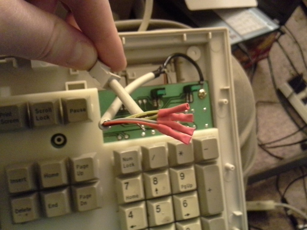
Dug through the ol' box of Keyboards, pretty certain I didn't have an XT keyboard (which is not at all compatible with AT/PS2)... and lucked-out with a nice surprise:
![]()
So, of course, this project was meant to be, right?
First things first, apparently somewhere down the road I thought it more likely I'd use the cables (I was kinda into MIDI, at the time... same connector) than that I'd use these old beat-up keyboards... so years ago I cut most of my grubby keyboards' cables and stored them separately... (and numerous times I'd thought to just dump that box of keyboards, glad I didn't). Dug through that box of cables and found exactly the right one... (!) Hadn't even been repurposed!
![]()
I can't recall what the result was, powering the system up that first time... was it a nasty long beep, or...?
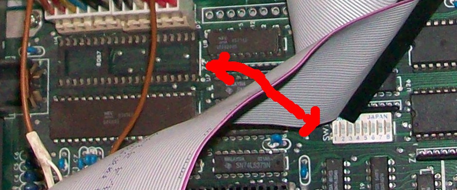
Anyways, turns out the switch-settings on the motherboard were incorrectly set for an FPU. (Did I desocket the 8087 FPU long ago, explaining why I found one in my "unsorted chips" bin a few weeks earlier, or did the switches get bumped in all those years stored in a box with dozens of other scrap PCBs and no anti-static bags?)
Changing the switch settings (nicely-documented on the web!) solved that problem!
Next, the video card wasn't syncing up with the TV... In fact, for quite some time no video was showing up at all... until finally I connected it straight to my old CRT TV--rather'n an LCD, nor through a VCR--when I saw something, but not legible.
![]()
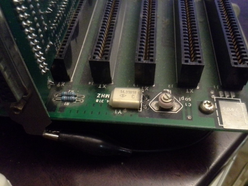
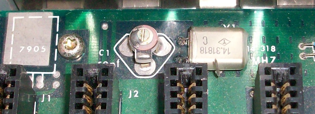
So I fought long-and-hard with the color-burst adjustment capacitor on the motherboard... It seemed to get better with adjustment but never quite legible, so I cut the trace between the capacitor and the crystal, and experimented with series caps. No go, there, so tried a parallel cap, still nogo... Finally replaced the crystal altogether... Still nogo.
![]()
Note that the board is labelled 14.318MHz, as I recall its crystal also being labelled. I grabbed a 14.31818MHz crystal this time.
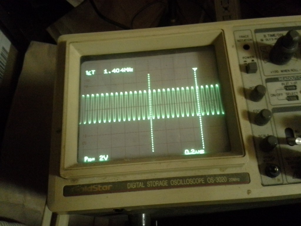
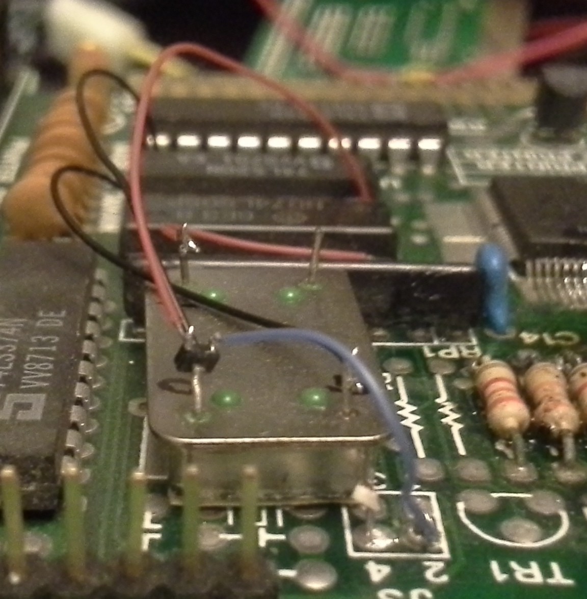
I 'scoped it out... and I can't explain this, but my 'scope showed 14.04MHz, even after these changes, and varying the capacitor had only a *tiny* change in frequency. 14.04MHz is *way* off, so I figured maybe the capacitor was old-and-crusty or something... maybe the loading of the driver circuit varied elsewhere... I dunno. Another thought, early on, was that the original crystal might've "cracked" in the decades of abuse, which would detune it, right?
![]()
I'm sure I've checked this countless times... That's ten peaks, 14.04MHz. I don't get it, and you'll understand why, when we get through this ordeal...
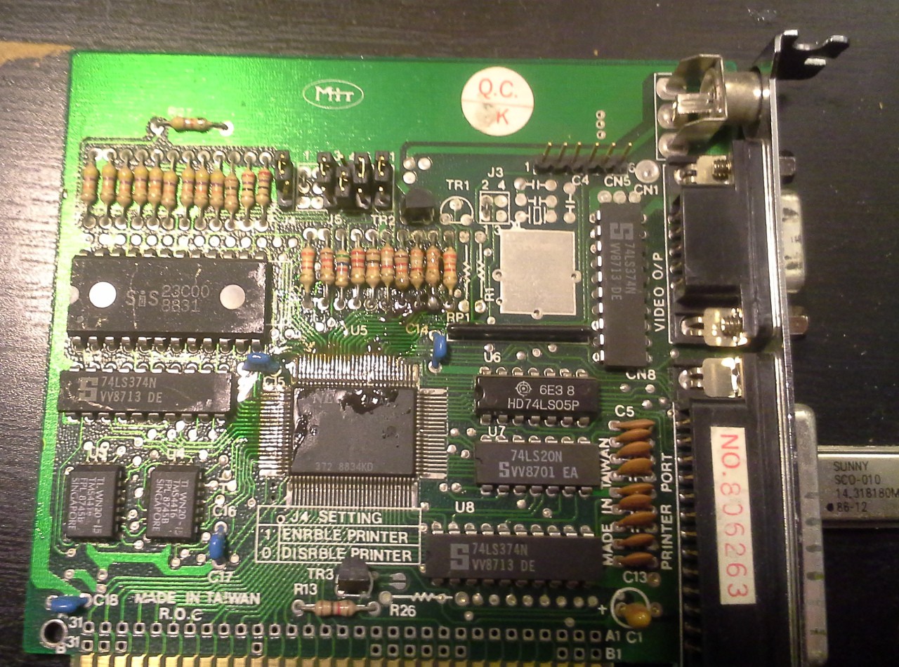
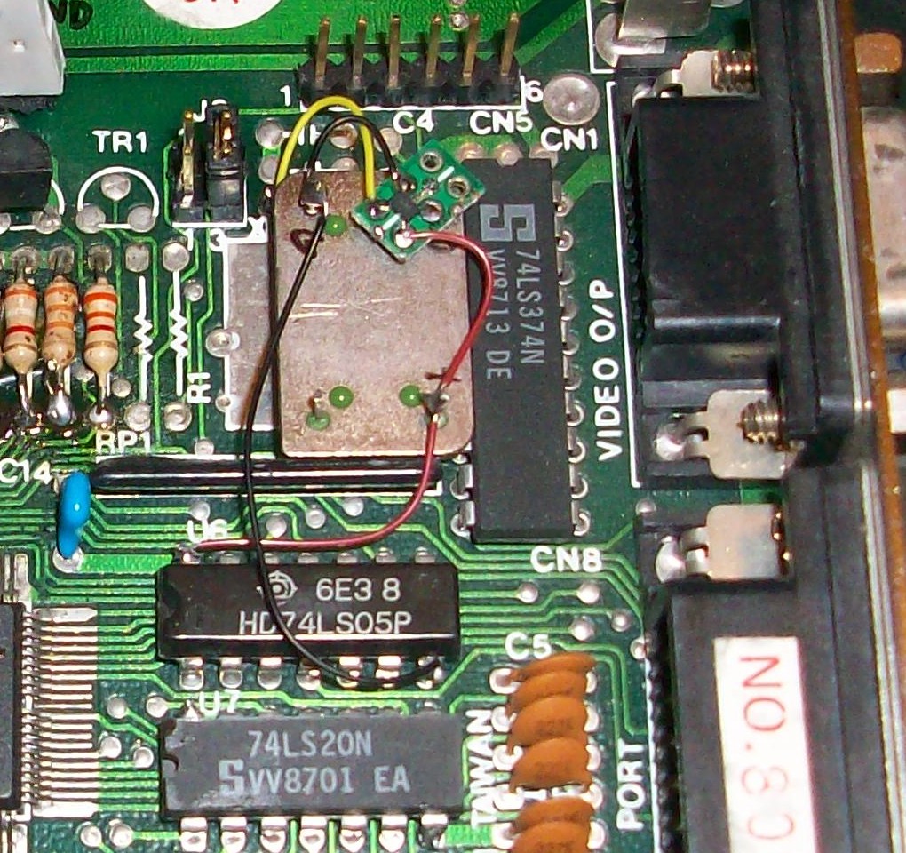
The CGA video card had an unpopulated space for a crystal, as well... I followed the traces and it seemed that there was a soldered-in wire where there could've been a set of jumpers to select either the clock signal from the ISA slots, or from the onboard (unpopulated) crystal's unpopulated circuitry... Since I didn't know what support components were necessary, and since the signal coming from the ISA slot was 0-5V, surely I could insert a crystal-oscillator with 0-5V swing, instead...
![]()
I dunno how it's possible, but the output from the crystal-oscillator wasn't strong enough... so I inserted a 1-gang 74AHC04... and even then the signal strength wasn't enough.
Turns out somehow I managed to rip the output signal off the board. (And didn't notice when I resoldered it to the '04?! Besides, it's not even visibly broken in this image!). Who knows, maybe the oscillator alone would've worked.![]()
That was a bit wonky, and was only a temporary-experiment, and once I measured a strong signal output I soldered it up right-er.
You can see the newly-installed jumpers to select the clock-source...
The result was *exactly* the same... there was a signal going to the TV, but it wouldn't sync, and was completely illegible.
The board was nastily corroded around the "GPU", and the resistors above it, so I spent some time cleaning that up. The resistors were especially hard to clean, I just kept throwing a bunch of flux at it and scraping with the iron's tip. What I should've done was remove and replace them. But metering it out from the other ends of the traces seemed right, so they couldn't be the problem (for now)... right?
Still no change.
Finally I just gave up and started swapping random (unlabelled) jumpers on the CGA card, 16 possible combinations... But sure enough it worked... second try. Maybe it was set for PAL?
...
Stepping back, now that it's functional with a crisp picture, I try adjusting the capacitor, again, try the two different crystal-sources, etc... and... basically all that work was completely unnecessary... the (new) on-board crystal and capacitor did the job, once those jumpers were set. Weee! (BUT WAIT! My friggin' scope was showing 14.04MHz, no?! WTF?!).
But I'm leaving my deadbug crystal-oscillator hack, dagnabbit!
Now... the thing needs a floppy controller, so I dig one out that looks to be right for the system... It's a bit beat-up (stored as scrap-PCB), the battery-socket's been ripped-up, but otherwise nothing appears shorted or broken... Plug it in and... the power supply won't turn on. Fine, scrapped.
I've another idea I came across while digging through the boxes:
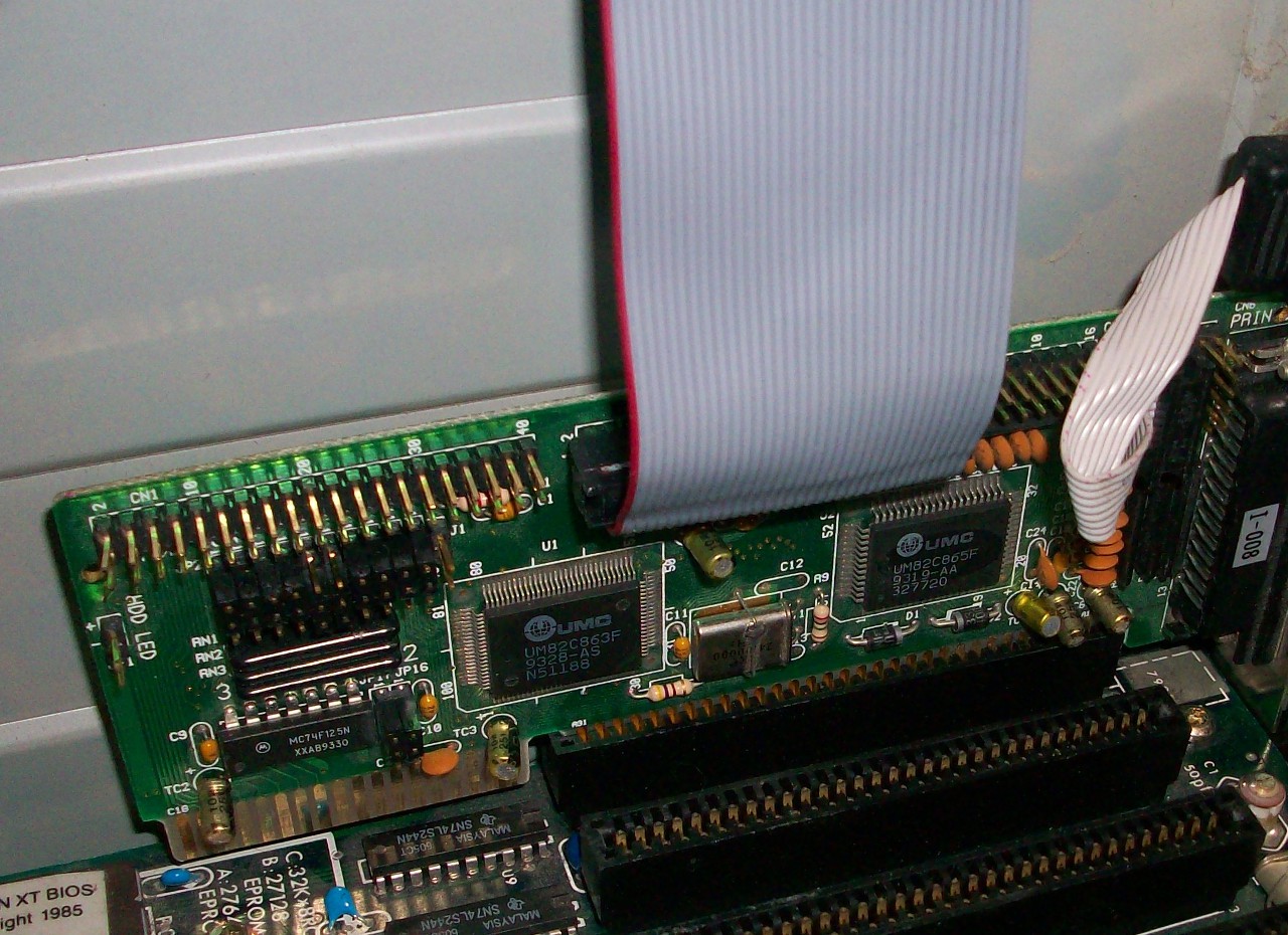
It's a multi-function card, I think from the 386, maybe 486-era. But I followed the traces on the 16-bit edge-connector, and they *only* go to the IDE connector! So, disabled the IDE controller, and... seems to work-ish. The floppy drive reads when it's supposed to, the parallel port was detected, etc.
So, now, the floppy drive... Now *there's* a multi-day endeavor, and I didn't really take photos of the nitty-gritty.
I only have 1.2MB 5.25inch floppy drives... And, apparently, the XT BIOS doesn't like those (it was designed to work with 360K drives). Long story short, one of the higher-quality TEAC drives in my collection has a *lot* of jumper-settings, and some pretty decent documentation online, as well. And, within that documentation is, in fact, some jumper-settings making mention of XT computers. So it should work, right? I tried everything, learned a ton about the floppy interface signals, and more... But never could get that danged drive to work.
So I went back to the original floppy-controller, the one with an edge-connector for the floppy-cable rather than IDC connectors... Yahknow, dang thing looks like it was meant for this system, and even has some labels that match those on the motherboard. I even managed to find an old archive of jumper settings and whatnot for boards like these "Total Hardware '99", even managed to figure out, through that, what brand made the thing and what model it was, despite its not having any markings... Turns out the problem with the power supply was simple, one of the bulk-capacitors right at the ISA connector had shorted-out... I just wiggled it until it broke off and it powered-up fine. But... still nogo with my 1.2MB 5.25in drive.
Finally I gave up and tried something that seems utterly-ridiculous, based on what I'd learned about the signals... something I'd read passingly on a forum, and dismissed as absurd. Allegedly you can connect a 1.44MB 3.5in floppy drive to an XT, and if you use 720KB disks, it allegedly will work.
Whelp. Sure enough... It works. I can't explain it, despite everything I'd learned about floppy-controllers and signals, about data-rates and spindle-rotations, nevermind bytes-per-track... but it works.
And, yahknow, I can write 720K 3.5in floppies in my friggin' USB-floppy-drive. Wee!
------
OK, so now I've a bootable system!
All I really needed to do was rewire the keyboard, switch the well-documented switch-settings properly on the motherboard, randomly switch around some undocumented jumpers on the CGA card, and believe something utterly-ridiculous I read on a forum. (Why does this feel a bit like the solution to MYST? Certainly playing that again would've been more fun than doing this!) Instead, at this point, I'd already invested well over a week and many sleepless days into the danged thing...
weeeee!
------
Oh, and the multi-function 16-bit ISA card works fine in an 8-bit slot, so that's pretty cool.
-----
So, now, I have this brilliant idea that maybe if I install a SCSI card, I'll be able to boot from a SCSI hard disk.
This ordeal... another "meant to be, right?" scenario. I plugged the thing in, and sure enough, during the POST procedure, the thing goes through its process of detecting drives. NICE!
Got a 1GB SCSI hard-drive erased and loaded up with most of my 8088-compatible software... oh man... I did this in another much-newer system I built, which I haven't even *begun* to talk about, here... I'll letcha look at those old logs, this was supposed to be just photos... Here's one from that log, wherein one of my newer pentium-based system attempts flat-out refused to work, and instead just stared back at me.
![]()
Anyways, loaded the thing up on a different newer system which was booting from that drive on the controller-card which was auto-detecting drives on the XT... but it wouldn't boot on the XT.
So, some forum post, and some pretty cool dude... apparently the newest ROM available for this SCSI card (v8.5, which I happened to have) doesn't work with XT computers, but v8.2 does. And that cool dude just happened to upload v8.2.
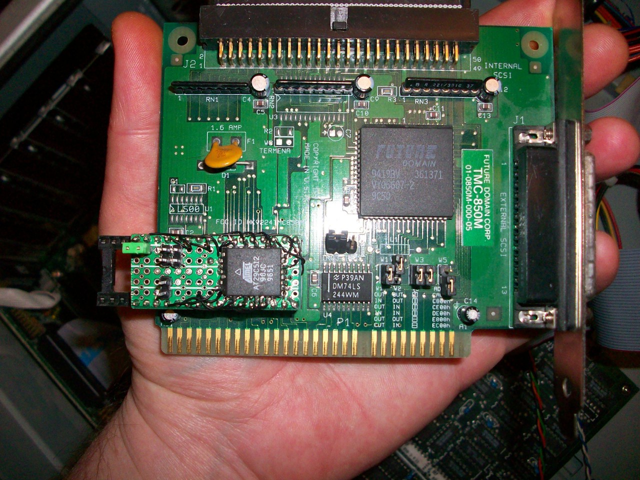
So, now... I've got to load an EPROM or something with the v8.2 ROM. I don't have a UV-eraser, at this point, so I built this adapter for a FLASH chip (shown in my universal-chip-programmer):
![]()
And then the ordeal with the chip-programmer... Actually it's a pretty cool story. I lost my chip programmer's "personality module" for programming [E]EPROMs a while back, much to my dismay... So it wouldn't program anything until I replaced it. I did a *lot* of unfruitful searching for a replacement long ago, so this time I wound-up emailing a guy who mentioned having this programmer in a forum-post SEVENTEEN YEARS AGO, and within two hours he sent me the needed information to recreate my lost module (no kidding).
That story is explained over at: https://sites.google.com/site/geekattempts/misc-notes/megamax-programmer
But suffice to say, I replaced the lost personality-module with a home-made one:
And, at this point, I discover that my programmer has some blown transistors (WTF, how'd that happen?!) So, a bit of troubleshooting in there, and two transistor-replacements later, (and we're talking *days upon days*, at this point) we've finally got a programmed v8.2 ROM for my SCSI card to boot my PC/XT computer from a 1GB hard disk...
Yep, it overhangs the socket. Yep it's mounted in another socket. I managed to press-fit the thing using standard 0.1in headers into a regular-ol' DIP socket (using an aluminum-can crusher, no less), such that the socket's much skinnier pins would fit into another socket without requiring much force. The jumpers allow selecting between "programming mode"--where it appears as the 512Kb FLASH chip it is to the programmer--and "BOOT ROM mode"--where it appears as the original 16Kb EPROM to the SCSI card. (Isn't it nice they've designed ROMs like these to have nearly identical pinouts, despite the increasing number of pins necessary for addressing larger devices?).-----------
ALRIGHT!
At this point the whole thing's pretty much functional... But I've been running it as a mess of wires and PCBs strewn across my coffee table for weeks... Time to put it in a case... OF COURSE I didn't save the original case... that'd've been ridiculous... Who could possibly want an IBM PC/XT in/after the era of Pentiums?
So, I've chosen an ATX case. And an ordeal with the power-supply... My original AT-style power-supply had cables which were too short. So, amongst the first things (besides drilling out the necessary holes, etc.) is to make a power-extension. But, yahknow, instead of actually making an extension, which would've been as easy as just using a bunch of wirenuts... I decide to use an ATX power-supply, instead.
Well, boy-howdy, that shoulda been easy enough, but instead it wound-up being an ordeal of several days. (also logged in past-logs).
Basically the white "blob" is my flip-flop circuit that turns on the /PWR_ON signal for the ATX supply... Pretty simple, in theory. Not so much, in practice... The flip-flop circuit takes the regular-ol' pushbutton from the front-panel, and also outputs the signal for the power-LED.Now, ridiculously, this ATX case has only one LED on the front... a dual-color one for indicating both power and hard-disk activity. That's great! No... It's a common-cathode, and my hard-disk activity-output requires common-anode.
So, now... I've taken it even further, and decided to replace that LED with an RGB-LED WEEE! Now I can choose which color indicates power (green) and which indicates the hard-disk (Blue... OOOOhhhh blue-LEDs in a PC/XT computer!). And maybe even find a use for the red, as well. But, of course, my multi-color LED supply just happens to have been from the very beginning of the multi-color LED era... back when a single RGB LED cost nearly $6. And so it requires *two* blue LEDs (internal) to light up even remotely bright enough to be seen over the green... and even the green's not particularly bright... and the designer of this ATX case (who will remain unnamed) used a light-pipe system which doesn't really do a very good job of piping light... so basically all that work and it's barely even visible unless you're staring *right* at it, from a +/- 10 degree viewing-angle. Weeee! But, I suppose that makes it at least a tiny bit more period-accurate, anyhow.
Really, this was supposed to just be pictures...
Alright, next ordeal...
The stupid ATX case, again... The design of the bracket-mounts is like none other. Instead of using screws to screw the ISA/PCI brackets down, it has some sort of springy-lever which clamps them down. Seemed cool, at first. But turns out it's a bit faultily-designed. That springy-clamp-thing actually blocks the tops of the brackets. Which blocks my CGA card's Composite output. So now...
Low and behold, there's another unpopulated header on the CGA card for a separate composite output. Easy! (No, that stupid panel-mount RCA-jack cannot be mounted without soldering *after* the fact.)(Maybe I should build a light-pen!)
------
Now, a fully-functional PC/XT-clone in an ATX case with a blue LED and a 1GB hard disk... What on earth am I gonna do with this thing?
------
Tonight: Installed a ZIF socket in place of the BIOS ROM, and found another XT BIOS ROM in my old EPROM collection... So now I've the original "American XT BIOS" and a "Super XT BIOS" to mess around with. The Super XT BIOS seems to boot my machine just fine, and also shows RS-232 cards in the device-listing during boot (which the original didn't)... so that's cool. (Heh, wouldn't it be funny if it worked with 1.2MB 5.25in floppy drives?)...
Received a "germicidal" bulb to build a UV-eraser... So now the SCSI ROM is now a regular ol' EPROM... maybe I'll use that FLASH chip for my BIOS experiments.
---------
More in-depth writings on the ridiculous experience this has been:
https://hackaday.io/project/18868/log/50347-to-up
- "My home is Tore-Up!"
- Newer System Adventures, and conscientious-objection
- Findings on old hard drives
- Floppy ordeals
- CGA WEEE!
- Finding that keyboard "meant to be!"
- Rearranging led to a new workbench! (which is now covered with storage)
https://hackaday.io/project/18868/log/50426-eepromer-adventures-and-more-realistic-goals
- "and it *still* didn't occur to me that I have an EEPROM-programmer, in my possession."
- the "miracle" communique for my personality-module replacement
- (more realistic goals for the *actual* project)
https://hackaday.io/project/18868/log/50648-it-boots
- "(Can it be called a "machine" if its guts are strewn across a table?)"
- "Hack" to repurpose a USED EPROM without a UV-Eraser
- Discovery of EEPROMmer's dead transistors
- "debug.exe"
- 736KB? Screw 640!
https://hackaday.io/project/18868/log/50774-casing-ttl-fail
- Reclaiming my coffee table - An ATX case
- ATX power-supply decision
- Simple Flip-Flop Circuit
- Pull-Downs, CMOS-expectations, and old-school TTL = fail
- Really, quite a lot about old-school TTL... sheesh
- This shoulda been easy!
https://hackaday.io/project/18868/log/50780-open-collector-fail-the-atx-power-switch-saga-continues
- Adding a NPN transistor to the output, to make it "open-collector"
- Installing a PNP by mistake
- Learning a ton! Didja know a BJT can be turned on by VCB rather'n VEB?
- This shoulda been easy!
- Shoulda left it, it actually worked with a PNP in an NPN's place, but wasn't "normal".
-
A better idea 2.0... uC's *as* ROM
01/12/2017 at 11:49 • 4 commentsDuh... as mentioned in a previous log...
#A 4$, 4ICs, Z80 homemade computer on breadboard
has some great ideas...
I still like the idea of actually using original PC/XT peripherals for this project, I dunno why exactly, but that's kinda the point.
BUT... one of the things @Just4Fun also did over at that project was to implement the ROM/BIOS in an AVR. The AVR's not *executing* the code, since it's Z80 code. It's making it available as though the AVR was a ROM.
Welllll... sheesh... here I am thinking about piggy-backing a ROM on top of the original ROM... (last log) Why not use an AVR *as* the ROM?
Plausible, maybe even probable. AND, most-importantly, In-System-Programmable!
------
So, realistically, I've a bit of an AVR-shortage 'round here... I *might* have a spare 644P with a few blown I/Os that'd work, but otherwise we're talking 8515's with enough pins and only 8K of storage (though if I write 8K of assembly, that'd be absurd). So, another option is some PIC32's I've in-stock.
I hesitate to use these for *this* project, because half of the point is to see what a lowly 8-bitter can do. But I don't see using a PIC32 as a ROM as being out of the spirit of the original intent... since the same could just as easily be done with an EPROM and a ZIF socket. It'd mainly just be a time-saver.
Why not, eh?
-----
Oh, and I could probably fit the original ROM as well.
:/ I kinda liked the idea of piggybacking, but this makes a lot more sense...
------
FOOL!
Those're 3.3V-only! ...
---------
alright, the 100-pin TQFPs I have have *just enough* 5V-tolerant pins... That's a bit ridiculous, but doable I spose.
Improbable AVR -> 8088 substitution for PC/XT
Probability this can work: 98%, working well: 50% A LOT of work, and utterly ridiculous.
 Eric Hertz