CYUL
CYUL-
A year later...
01/17/2024 at 02:54 • 0 commentsSo, I learned another, not so funny lesson. Someone liked one of my designs so much that he went out, set up shop and started to sell them without even giving credit...
So, from now on, I am changing the license for all my designs to CC BY-NC-SA 4.0. You can build one for yourself, or your best friend, or your mum, but you cannot sell it as a product. If you change something, think it's genius, and absolutely want to share what you have done, you have to credit me and it has to be shared under the same license.
What a world...
-
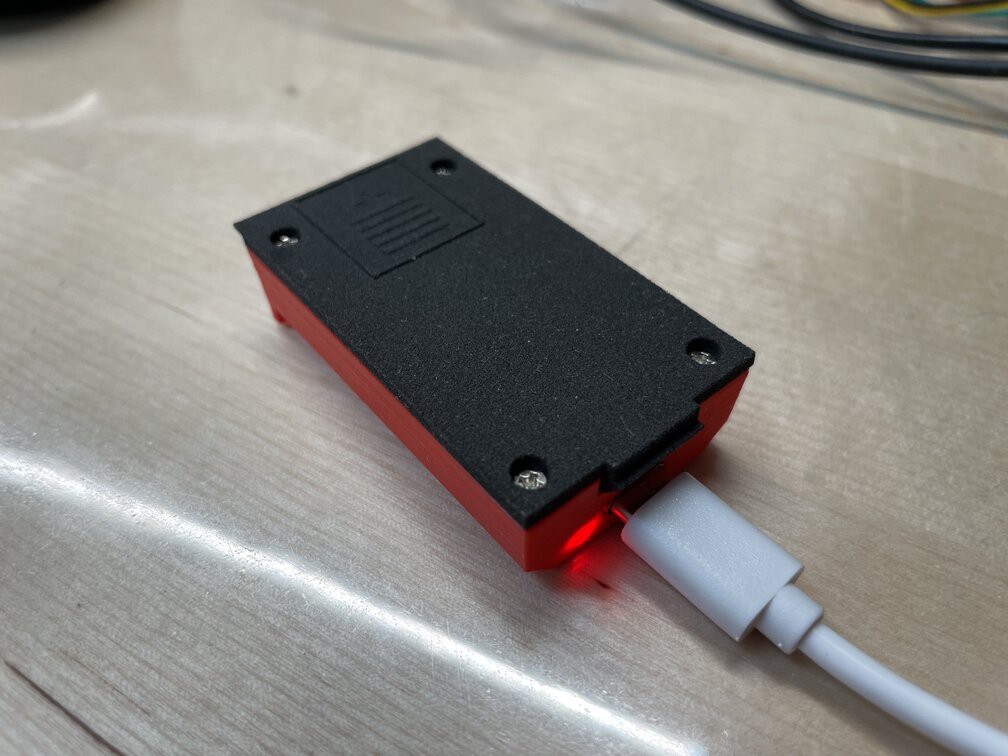
It's alive!
02/12/2023 at 15:37 • 0 commentsPCBs were received from the fabrication house and they work!
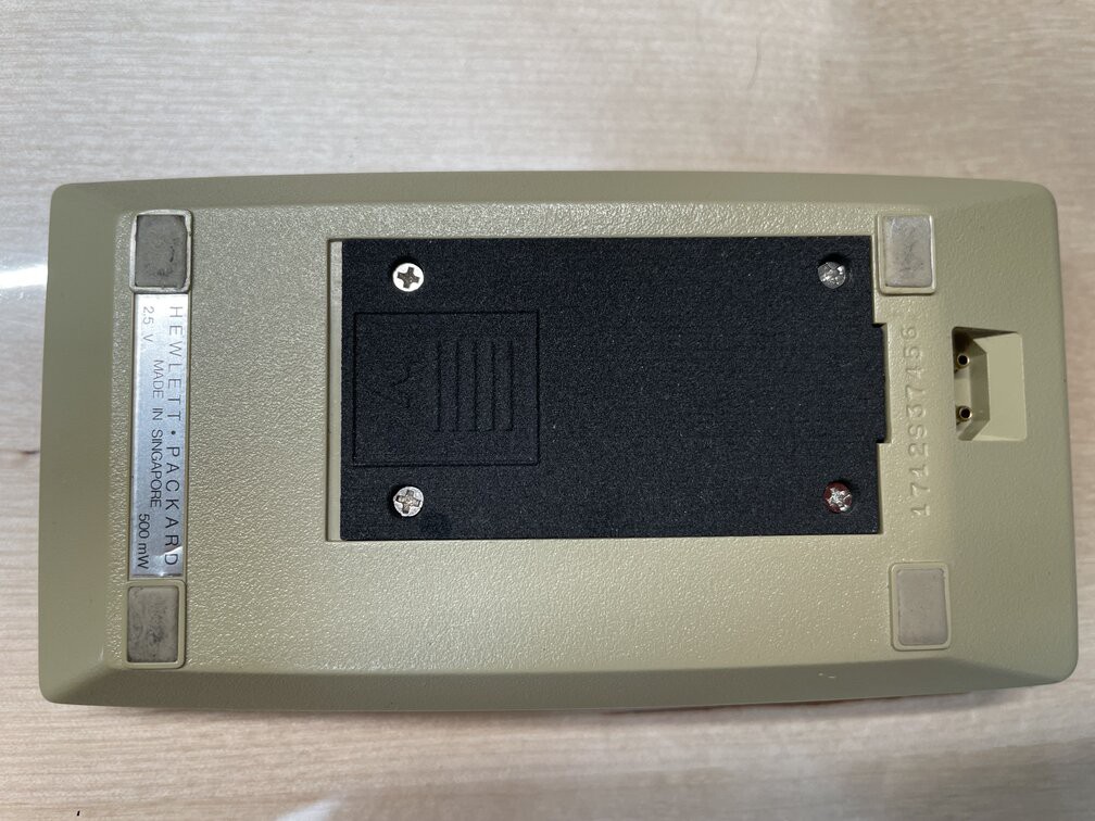
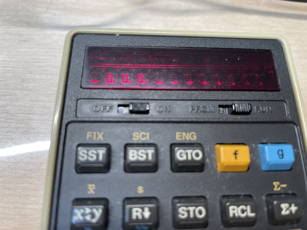
Here is a photo of the battery pack being charged inside a temporary housing that I 3D printed using my trusty Ender Pro while waiting for the laser sintered parts that I ordered, then another one with the pack in place (it is exactly as difficult to remove from the calculator as the original), then a picture of a happy calculator.
![]()
![]()
![]()
LED displays take such a weird hue in digital photos, what's this about?
Also, why is it so difficult to find beige/cream/ivory/bone white PLA anywhere?
The next step is to integrate a Qi receiver in there. I looked around and there doesn't seem to be any hobbyist friendly solution. I am currently looking at Texas Instruments (oh, the irony!) BQ51050B chip. The datasheet is very unhelpful. Wireless looks hard! Thankfully that (expensive!!!) chip is available in a 20 pin VQFN package. Whereas I was soldering most of this by hand, soldering this much smaller package of a chip seems like a challenge. It should be feasible with patience, some solder paste and a hot plate (literally a hot plate: I plan to use our ceramic stove). I would use a 20mm coil.
If anyone has hints on how to calculate C1 and C2, or a working design I could reference, please hit me up.
-
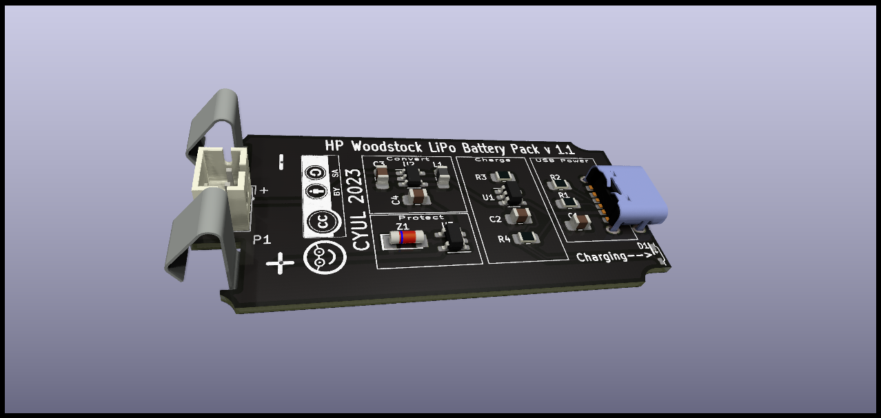
First PCB. Lessons learned.
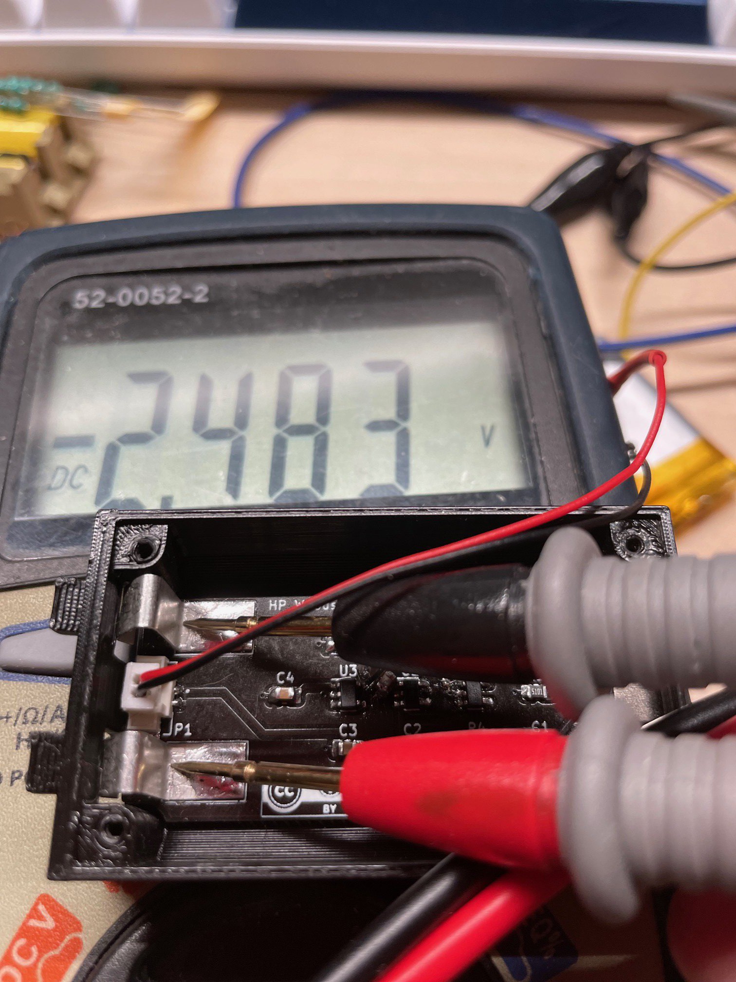
01/24/2023 at 02:44 • 0 commentsI got the first batch of PCBs back from JLCPCB and found out several mistakes.
- I had inverted the two 2.5V contacts. Positive is negative and vice versa. I changed my mind in the middle of the initial design and moved the PCB to the bottom of the case instead of right under the top of the enclosure, and this happened... See the minus sign on the multimeter display? Shouldn't be there. Grrrr...
- The spring contacts do not touch the bottom rivet of the contacts inside the calculator. Rather they make contact on the top part of the rivet. It works but barely. I am not sure my HP25 is typical, because that's my only Woodstock, but the contact rivets are very very small. I wonder if it's normal.
- The buck converter stalls when you turn the calculator on (too much current is drawn at once) and only recovers to about 1V vs. its nominal 2.5V
- The 1.25mm connector is way too small. It works with small batteries, the 200 mAh kind that run mini drones, but that won't work for larger batteries, the wire are just too big for those connectors.
![]()
So I went back to the drawing board:
1) and 2) I reworked the PCB to solder the contacts to the bottom of the PCB (and corrected the polarity issue). I changed the outline of the board to hopefully simplify construction. There are notches to guide the contacts when soldering them from the bottom. I wrote + and - in the calculator compartment to remind me.
3) I found someone who had a similar problem with the ADP2108. It turns out, at 3MHz, every millimeter of PCB trace counts. I solved the problem on the prototypes by soldering a 4.7uF capacitor right on the converter pins. Back to the drawing board, again, to change the PCB and shorten the traces. While I was at it, I completely redesigned the layout.
4) I changed the 1.25mm Molex connector for a 2.0mm JST connector. It's going to be tight but it (seems to) fit.
Now there is a new iteration of the enclosure to make space for the battery contact tabs on the bottom (wall thickness has to be at least 1mm, so I just made a hole) and also, since the through hole of the JST connector is smaller than the SMT equivalent, I had to leave space for the two prongs at the bottom of the PCB.
The order for a new PCB is at JLCPCB. Waiting for the first iteration of the enclosure that goes with the 1st PCB. We'll see if that would have worked mechanically.![]()