ziggurat29
-
20230212c -- Delays and cycle counting
02/15/2023 at 19:42 • 0 commentsThere are a couple delay routines in the firmware, so I set out to determine how long they are for. This means tallying the cycle count, and understanding the relationship between the external oscillator and machine cycles.
On the 68HC11, the external oscillator is divided by 4 to yield what is called an 'E-cycle', which is the machine cycles listed with the instructions. On this board, an 8 MHz crystal is used, so the E-cycle rate is 2 MHz (500 nsec).
An internal delay routine:
F623             sub_F623:
F623 18 CE FF FF     ldy     #$FFFF     6 cy
F627             loop_F627:
F627 18 09           dey                4 cy
F629 01              nop                2 cy
F62A 26 FB           bne     loop_F627  3 cy
F62C 39              rts                5 cy
The loop executes 65536 times, so the net result for this routine is 589,835 cy, or 0.294918 sec.
An outer delay routine invokes this a couple times:
F61E             sub_F61E:
F61E 8D 03           bsr     sub_F623   6 cy (+ 589,835 cy)
F620 8D 01           bsr     sub_F623   6 cy (+ 589,835 cy)
F622 39              rts                5 cy
So this routine takes 1,179,687 cy, or 0.589843 sec.
This routine is referenced quite a bit throughout. Both of these delays are quite long for something like key debouncing, so they surely are not used for that.
-
20230212b -- Photos, Keyboard
02/15/2023 at 19:35 • 0 commentsAs mentioned, my friend [Eric]@EricHertz indulged with some better pictures. Examining the keyboard connectors shows one set at J4 of 16 contacts going to a set of 16 diodes that are then go to the output side of two 74HC574. This is sane for column (or row) drivers of a classic keyboard matrix design. (The diodes prevent back flow if you hold more than one key down on different columns (or rows).) (I don't know the physical layout yet, but that doesn't matter yet.) The other connector at J5 consists of 13 contacts, but examining the board, I can see that 5 are grounded. The remaining 8 go the input side of a 74HC573. They also go into a resistor pack and a 74HC30. So these are surely the row (or column) sense. The resistor pack pulls up the lines, and the 74HC30 serves as an indicator 'key down' when any row goes low. All of this is sane.
The gist is that when you want to scan for keyboard, you:
- set one bit of the 16 column lines low
- see if the output of the '30 is high; if so there is a keydown on this column
- read the '573. The 0 bit will be the row for which the key is down
And since this is a primitive design, you're going to need to do key debouncing in software. So whenever I find the keyboard routine, I expect to see some delay loops. I also expect to see some translation of (row, column) pairs into ASCII characters. I did find some text:
FB6C 32 20 61 62+a2Abcdefghijklm:fcc "2 abcdefghijklmnopqrstuvwxyz"
FB6C 63 64 65 66+                fcb 9
FB89 31 32 33 34+a1234567890:    fcc "1234567890"
FB89 35 36 37 38+                fcb $D
FB94 33 20 60 2D+a3_@_?:         fcc "3 `-=[]\"
FB94 3D 5B 5D 5C+                fcb $27
FB94 27 2C 2E 2F+                fcc ",./~!@#$%^&*()_+{}|:<>?;"
FB94 7E 21 40 23+                fcb $22, $D
FBB7 34 20 41 42+a4Abcdefghijklm:fcc "4 ABCDEFGHIJKLMNOPQRSTUVWXYZ"
FBB7 43 44 45 46+                fcb $D, 0
which look like candidates for a translation table. I'm sure I did not break those strings up correctly, but I can fix that later. Finding a reference to those strings will be helpful in locating the keyboard routine.
-
20230212a -- Config registers
02/15/2023 at 19:33 • 0 commentsOne of the first tasks at startup is to configure the system, setting options for peripherals, interrupt enables, etc. Starting at the reset vector, I am wending my way through the startup code and documenting all the config register changes. This is tedious work going back and forth through the manual (and also having to learn a new assembly language!), but in the end it will provide useful information as to how the system is physically built.
-
20230211d -- ISRs...
02/15/2023 at 19:31 • 0 commentsThis device has vectors placed in the highest memory location. Following documentation, I labelled all of those. In this product it seems none of the nifty peripherals are used because the various associated interrupt sources simply go to a dummy handler that prints "SpurInt!".
OK, so now I need to get down to it. The start vector is a good place to start, since that should setup up the system. There's some configuration registers that control things. I will have to learn a new assembly language.
-
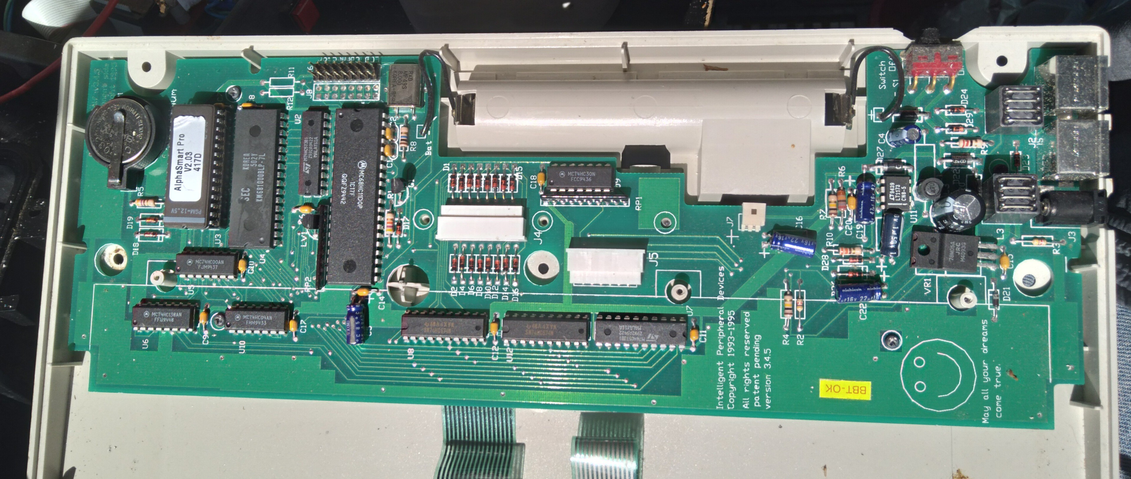
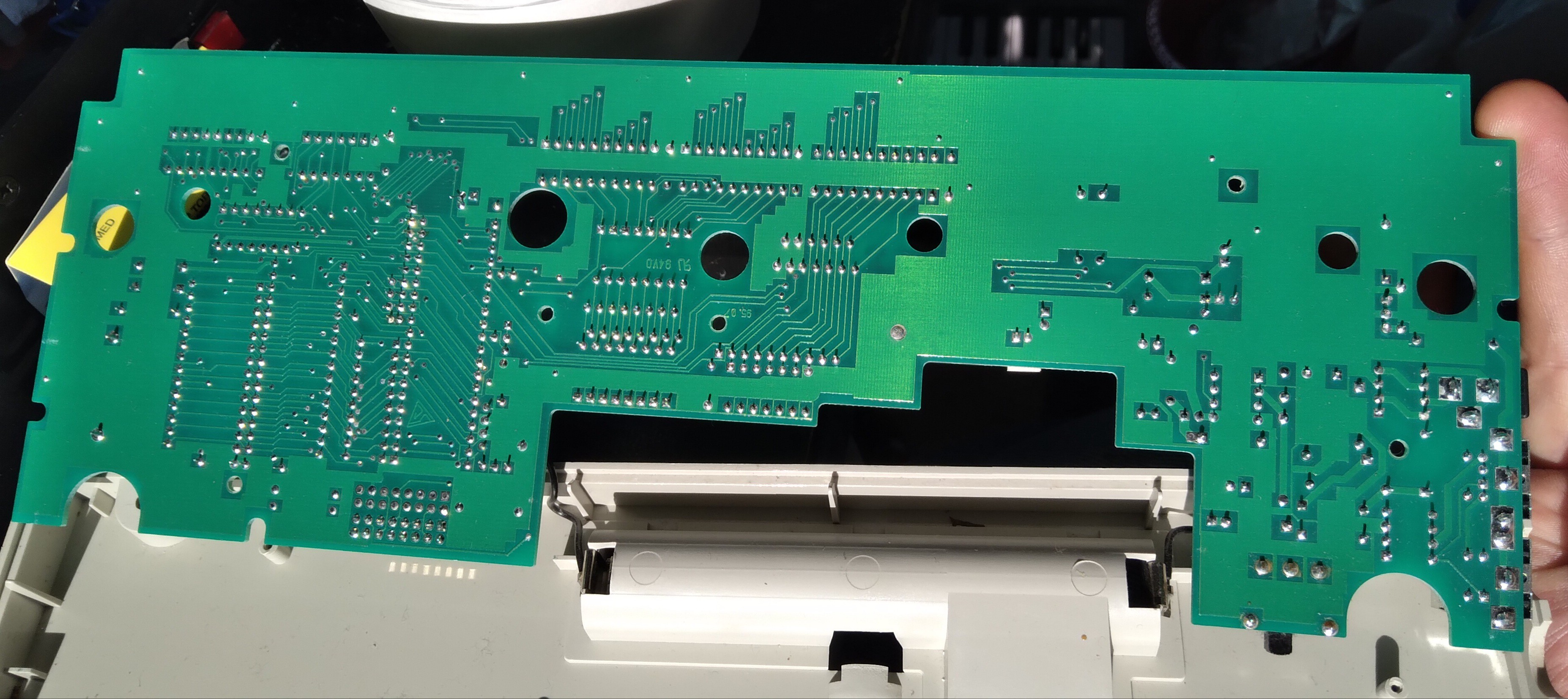
20230211c -- Photos...
02/15/2023 at 19:30 • 0 commentsMy friend [Eric]@EricHertz is too busy to fiddle with his physical AlphaSmart Pro, but he did indulge me to take some pictures that show the chip markings better. So this is a 'D0' variant of the 6811.
Topside:
![]()
Bottomside:
![]()
The main board is quite small, and looks like a two-layer board, so I might be able to do some significant work using these photos alone.
-
20230211b -- Textual healing...
02/15/2023 at 19:17 • 0 commentsOperating under the current assumptions, I first marked out what appeared to be text strings. It seems that largely a 'nul-terminated string' ('nts') scheme is used. Then I backtracked into the code to find address references to these strings. In the course, this led me to discover that there /seems/ to be a 'display text' routine at F669 which takes a pointer to the nts string in the X register.
F669             ; XXX show nts text @ X?
F669             xxxShowText_F669:
F669 E6 00           ldab    0,x
F66B 27 06           beq     locret_F673
F66D BD F6 74        jsr     sub_F674        ; XXX show char?
F670 08              inx
F671 20 F6           bra     xxxShowText_F669 ; XXX show nts text @ X?
F673             locret_F673:
F673 39              rts
Operating under this new assumption, it appears that there is a routine F674 that shows a character at the current cursor position, and advancing the cursor. I'll look into that more closely later. For now it is useful for me to cross-reference all references to this F669 routine and backtrack to all text messages, propagating comments. Associating text messages with routines gives us a clue as to the routines' purposes.
One thing you'll note is some patterns in how I generate hypothetical labels.
One is that I tend to put XXX on things that I am guessing. This gives me a visual indication that it is something I currently believe, but don't consider proven. So take with a grain of salt. When I later gain more or less confidence in the hypothesis, then I'll either remove the XXX or remove the label altogether. The label propagation feature of this disassembler is wonderful for automatically fixing that stuff up through the listing.Another is that I put the address at the end of the label. This is handy because it disambiguates what otherwise would be label collisions. So, for instance, if I had a candidate for 'showText' and then later found another one I like better as 'showText', I can effectively call them both that until I figure out which one is the 'real' showText, and the other maybe like 'showTextCommon' or something.
Doubtless you'll develop your own methodologies.
-
20230211a -- The feeling begins...
02/15/2023 at 19:13 • 0 commentsAs of late I have a bit of free time and am looking forward to a relaxing distraction of my peculiar taste in pastimes of disassembling ROMs of vintage equipment.
As fate would have it, my friend [Eric]@EricHertz has recently come into possession of a vintage typewriter of sorts -- The AlphaSmart Pro. (He finds the best junque!)
![]()
This device is a typewriter of sorts. I was created by some former Apple guys in the early 1990's and targeted the education market. The gist is simple: a portable keyboard with integrated LCD into which you can type documents.
Note 'document' means text only. Then you can connect it to a desktop-class computer, and it will emulate a keyboard, and dump the text out.
Apparently it was popular with some, the product went through several iterations, and the company was eventually acquired, and the product retired. I won't bore you with more history that you can find for yourself; e.g.:
https://en.wikipedia.org/wiki/AlphaSmart
Anyway, [Eric] mentioned having opened the device, and that the ROM was socketed, so I plead with him to dump it and send me the result. He had his own stuff to do, but happily he found time to indulge me.
This unit uses a 68HC11xx processor. I have never worked with this processor myself, so this will add a little fun to the mix.
First step is getting datasheets. The programming model looks particularly simple. It's a typical 8-bit device with a 64KiB address space. Reset vector is at the top of address space, so the ROM dump almost surely maps up there. The ROM dump is 8KiB, so for now I'm going to assume it all maps to E000 - FFFF. (Banking is a possibility, but I'm going to disregard that until proven otherwise.)
The processor had many variants, and the 'xx' I labelled indicates that I do not know yet which variation this processor is. Photos of the board are seemingly rare and too low res for me to make out the suffix, and I haven't found it called out in things like wikipedia, etc. The variant is important especially with this device because things like mapping of internal RAM are different across the product line. For now I'm going to guess it is a ROM-less version like the E0, since there is a big 'ol EPROM right next to it. This assumption may change as I start to dig in.
The RAM has large markings, so I can see it is a Toshiba TCS551001BPL-85, so that's 128KiB static RAM. That's way bigger than the address space, so surely that is banked in some way. I'm not too worried about figuring that out now because disassembly will start to provide clues. Normally, my friend [Eric] would buzz out the board and other things since he has the actual unit, but he's busy with other things right now, so I will hobble on.
The LCD is some 4x40(?), I'll punt on those details for now. I am going to assume the keyboard is some garden variety matrix done in software until I can figure out otherwise. There are two ports: one is PS/2 and the other is ADB. These are a quirky form of data transfer to a PC where the unit pretends to be a keyboard and simply dumps the contained documents as a series of keystrokes to the PC. lol!
I converted the Intel Hex to binary so I can whizz through it in a hex editor to get a quick lay of the land before getting into actual disassembly.
I can see at the end of the binary there is a block of 0x01's, which I presume are padding, and ending with a series of 16-bit ints, so I'm pretty sure those are the interrupt vectors. The last is the reset vector, and it is 0xe000, so this tends to confirm my suspicion that the ROM is not banked (if unbanked, it would map in at 0xe000).
I also found a text string 'This is the RAM valid signatur2'. This is interesting because it suggests that there is a routine somewhere that whizzes through all the RAM and computes a checksum. And if it whizzes through all the RAM, then it must do all the relevant bank switching as well. Because this will be a simple routine of linear access and accumulate, it will be easy to disassemble, and so will probably make it easy to figure out the banking scheme. So this is an early target of interest.
OK, time to fire up the disassembler. You can get by with disassembly to a text file that you then annotate -- and I do that sometimes with exotic processors -- but it really helps to have a nice disassembler that propagates symbol references and comments. It's difficult to stress how much more productive you will be with just those two features.
I am using an old copy of IDA Pro. It has 6811 support. It's ruinously expensive commercial software, though, so I can't give you a copy, alas. I will publish the textual disassembly, however. Aside: I have been meaning to try Ghidra for some time now, since it's free, and this would be a great opportunity, but I'm going to push that activity out yet once again. But if I make some headway, I may revisit that decision to kick those tires separately.
ROM Disassembly - AlphaSmart Pro
Wherein I disassemble the ROM from a vintage typewriter-thing