-
OmniSnort
01/06/2024 at 01:21 • 0 commentsWith the full base system working, it was then time to think about peripherals - in particular the digital tape drives used by the MCM/70. I've also got an MCM DDS-1000 dual 8" disk drive, thanks to Zbigniew, which is probably in need of some maintenance.
Part of getting these peripherals working is going to be seeing what happens on the Omniport as the peripherals run. But how to watch what's happening on the Omniport? I could use my Bitscope logic analyzer but it is pretty limited when it come so seeing what happens over a period of many seconds. What I wanted was something that could snort and record what's happening on the Omniport over a significant period of time . Hence, OmniSnort/
The idea was a bit of logic to catch the activity on the Omniport, a big RAM chip to save the captured data, and an Arduino Mega to look after sending the captured data back to a host computer. Simple enough, but It took me a while to get OmniSnort working to my satisfaction:
- OmniSnort version 1 was way too slow.
- OmniSnort version 2 worked but only recorded activity, not when it happened.
- OmniSnort version 3 records activity and also timestamp information. It timestamps Omniport activity with 100nS resolution, can monitor Omniport activity for up to seven minutes, and can record up to 87,000 Omniport events.
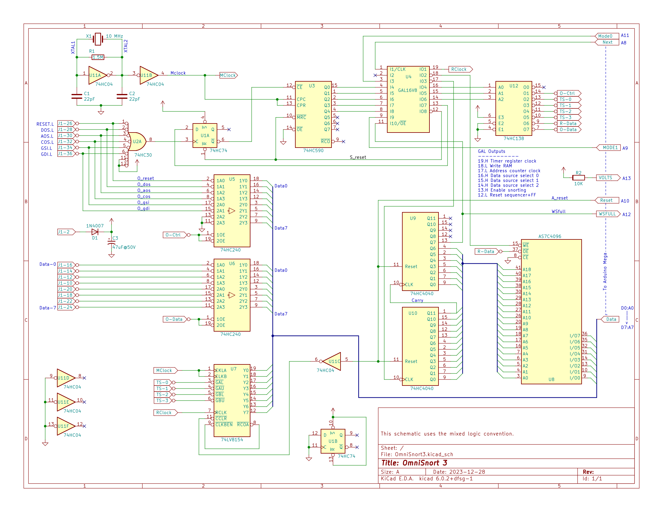
Without further ado here is the OmniSnort 3 schematic:
![]()
The Concept
The general idea is that we develop a 32 bit timestamp which advances at 10 MHz aka one count per 100 nS. We have a 512K static RAM chip into which we store data. When an event happens on the Omniport we store six bytes into RAM:
- The Omniport control lines
- The Omniport data lines
- Four bytes of timestamp information
As each event uses up six bytes we thus have room in RAM for 512K / 6 = 87,381 events. That sounds like enough.
How it works
In the upper left corner of the schematic, the crystal and friends generate a 10 MHz master clock "MClock".
At the bottom on the left is a 74LV8154 which is IMHO a fabulous chip which makes the design of OmniSnort *so* much easier. We use this chip to develop the timestamp to associate with Omniport events. It contains two 16-bit counters which have been cascaded to make one 32 bit counter. On command the count can be transferred to a 32 bit register and from there the four bytes of the register can, one at a time, be tri-stated onto the 8-bit output. We clock this chip with our 10 MHz MClock so it will be (2**32) / 10E6 = 427 seconds, or just over seven minutes, before this counter overflows. That also sounds like enough.
Middle-right-low are two 74HC4040 chips, 12-bit ripple counters, which we use to develop the 19 bits of address for the RAM.
Middle-high is a 74HC590 counter and a 16V8 GAL which together implement a really simple state machine.
The RAM, the Mega, and various other chips are connected to an 8-bit data bus, which allows us to get data in and out of RAM.
We want to be able to enable one and only one of seven different data sources onto the data bus, thus the GAL drives U12, a 3-to-8 decoder, which in turn can select one of the seven devices (or none) onto the data bus.
Way over hard-right are the connections to the Arduino Mega. The Mega can access the OmniSnort data bus. The Mega gets the following signals from the OmniSnort board:
- Wsfull: True if our RAM chip has filled up.
- Volts: The +5 from the OmniSnort logic, which in turn is derived from the +5.6 coming in from the Omniport. This allows the Mega to verify that OmniSnort is connected to an MCM computer and to verify that the voltage is sufficient for proper operation.
The Mega sends the following signals to the OmniSnort board:
- Mode0 and Mode 1: Sets the mode of operation.
- Next: When reading snorted data, advances the RAM address counter.
- Reset: Resets both the RAM address counter and the timestamp to zero.
The two mode lines provide for four different modes of operation:
- Snort: Activity on the Omniport is snorted and events are saved into RAM.
- Read: Events saved in RAM can be read into the Mega.
- Pre-write: Gets ready to let the Mega write to the current memory address.
- Write: Data from the Mega is written to the current memory address.
The last two modes are so the Mega can zero RAM prior to snorting so, at read time, it knows when it has reached "end of snorted data".
Operation when Snorting
When snorting, the GAL puts True on the D input of FF U1A. When there is any activity on the Omniport (that is, when any of the control signals goes low) then OR gate U2A clocks FF U1A. That in turn enables the CS/ input of U3 which then starts counting up at 10 MHz. Five of the count bits from U3 are fed to the GAL and this in turn drives the state machine through the non-idle states. We want to store six bytes into RAM and each bytes stored takes 3 states, thus 18 states. For each byte stored the three states are:
- Enable the appropriate data on to the data bus (Omniport control info, Omniport data, timestamp data)
- Write the data to RAM
- Advance the RAM address counter.
The last state of the last byte pulses the S_reset (State machine reset) line which clears FF U1A and which resets the state counter, thus idling the state machine and getting ready for the next Omniport Event.
The logic for the GAL can be found HERE.
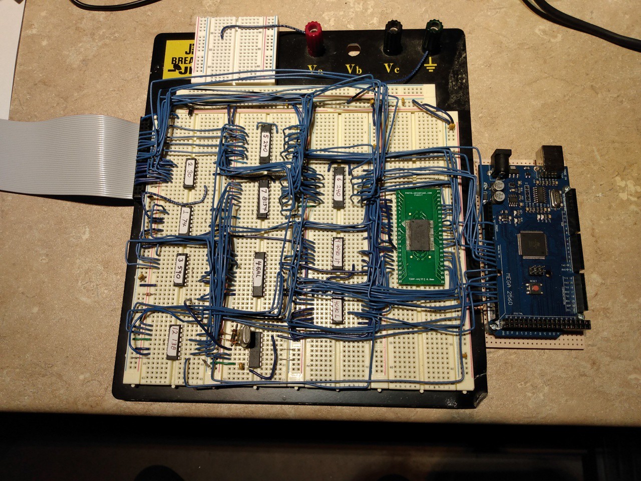
The working breadboard of OmniSnort version three looks like this:
![]()
The ribbon cable on the left connects to the Omniport. The RAM chip, being SMT, is up on the green adapter, while the Arduino Mega is on the far right.
With the breadboard version working, I made it into a PCB - sort of an oversize shield for the Arduino - which is now off at JLCPCB for production.
-
As a Single Board Computer
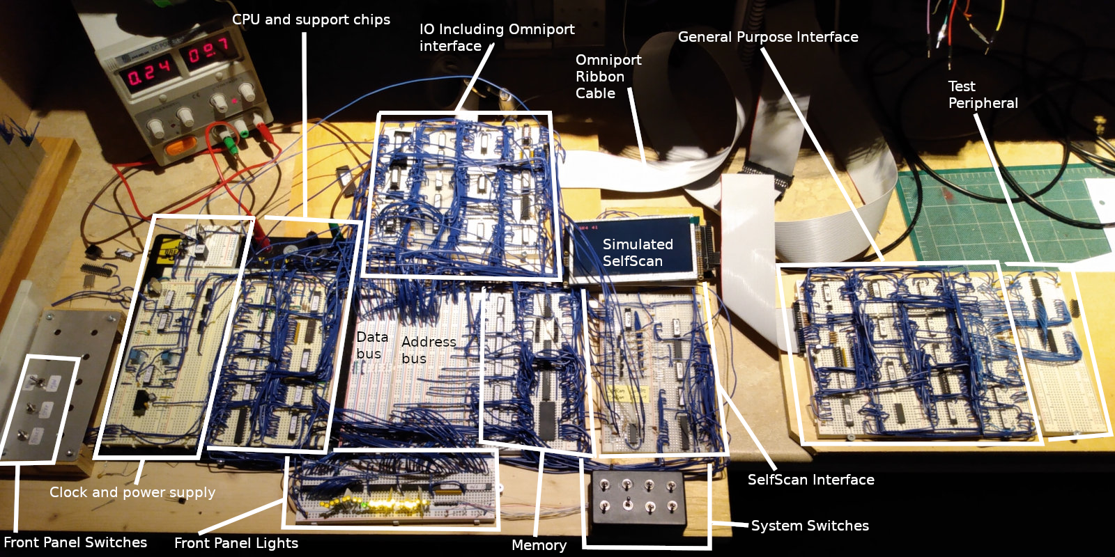
01/04/2024 at 01:43 • 0 commentsWith the Omniport interface, and the GPI board, and a test peripheral working that meant that the entire design was done. This photo shows the full breadboarded system with annotations:
![]()
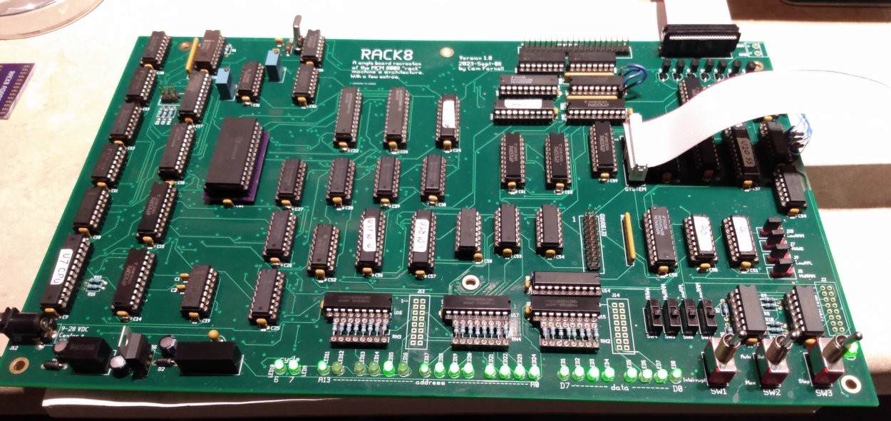
The next task was to turn everything - except the GPI and test peripheral - into a single board computer. This was a bit of an exercise, as there are 200+ components and 1500+ connections, which resulted in a six layer board. With this level of complexity I wasn't totally surprised that there were a few issues on the board, but none were catastrophic, and there were reasonable workarounds for all.
The board, populated and working, looks like this:
![]()
and it works as expected and runs MCM/APL. From my viewpoint, this was fabulous progress.
-
An Omniport Peripheral - Part 2
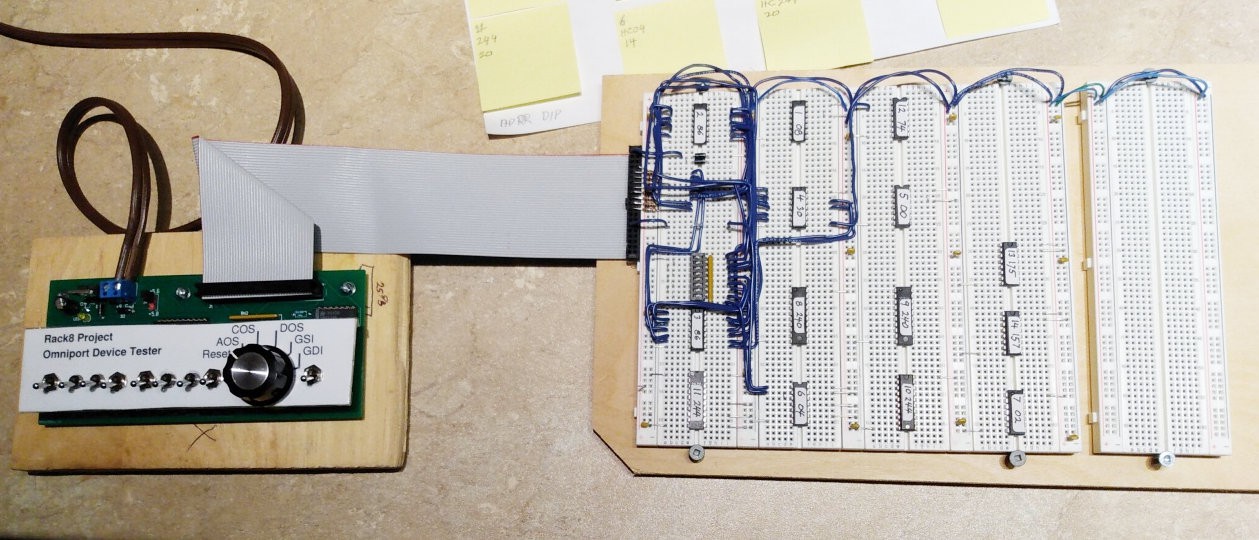
01/03/2024 at 22:59 • 0 commentsWith the schematic for the GPI board in hand, the next order of business was breadboarding it to make sure it worked. The photo below shows GPI breadboard near the start of testing. At that point the goal was to get the device selection logic working. To the left of the breadboard is the OmniTester, from the previous log.
![]()
It wasn't all that difficult to get the GPI working - It was pretty much just replicating the ideas behind the MCM schematic - and so in short order it was looking good.
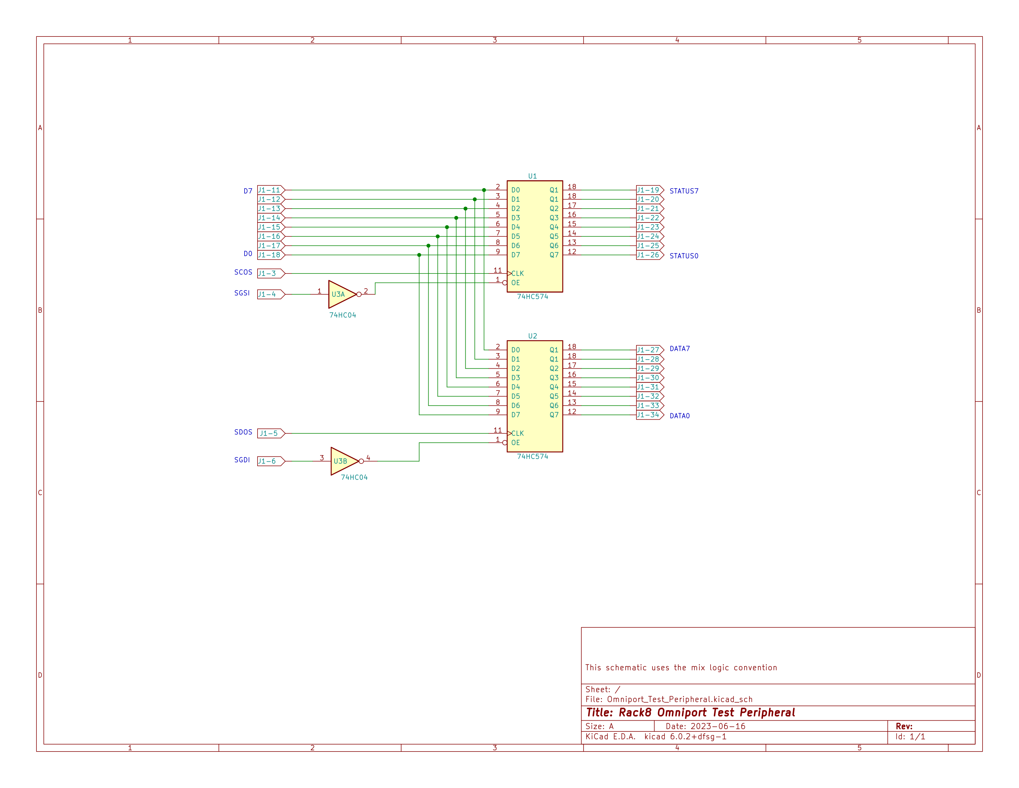
But then an actual peripheral was required to make sure it worked as intended, which resulted in the following schematic, which is pretty much "Hello World" as an Omniport Peripheral:
![]()
consisting of two 8-bit latches and a couple of inverters. When the MCM computer sends a command to the peripheral it is stored in latch U1. When the computer ask for the device status, the value in U1 is returned. When the MCM computer sends a data byte to the peripheral it is stored in latch U2. And when the computer asks for data from the peripheral the value in U2 is returned. Useless in practical terms, but just fine for verifying operation of the GPI card and the Omniport interface on the Rack8 machine.
The photo below shows the prototype GPI (the four breadboards on the left) and the test peripheral (the single breadboard on the right). The GPI is connected to the main Rack8 breadboard by the 40 conductor ribbon cable on the left.
![]()
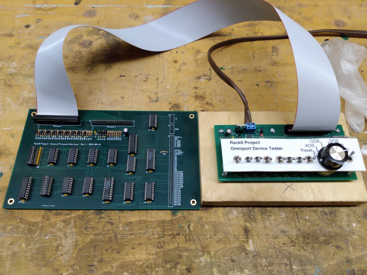
The test peripheral helped establish that the Omniport interface and the GPI were working just fine. With that done, it was time to turn the GPI into a printed circuit board. The photo below shows the printed circuit version of the Rack8 GPI board, connected to the OmniTester. The row of Berg strips on the far right of the PCB are for connection to the eventual peripheral.
![]()
-
The OmniTester
01/02/2024 at 01:51 • 0 commentsSo we are developing a GPI board, which can be used as the basis for MCM peripherals, at least partly in order to test the breadboard implementation of the Omniport. But then we would like something which is itself capable to exercising the GPI board, and by extension, to help test any peripherals we might build based on the GPI board.
Operation on the Omniport is coordinated by the six control signals generated by the MCM/70 computer. Pulses on those control lines have a specified minimum time but no maximum time. Thus it's possible to do static testing on the GPI board and on quite a few peripherals as well. For example the Hytype daisy wheel printer used by MCM could be driven at slow speed because it will cheerfully wait any length of time for the next command.
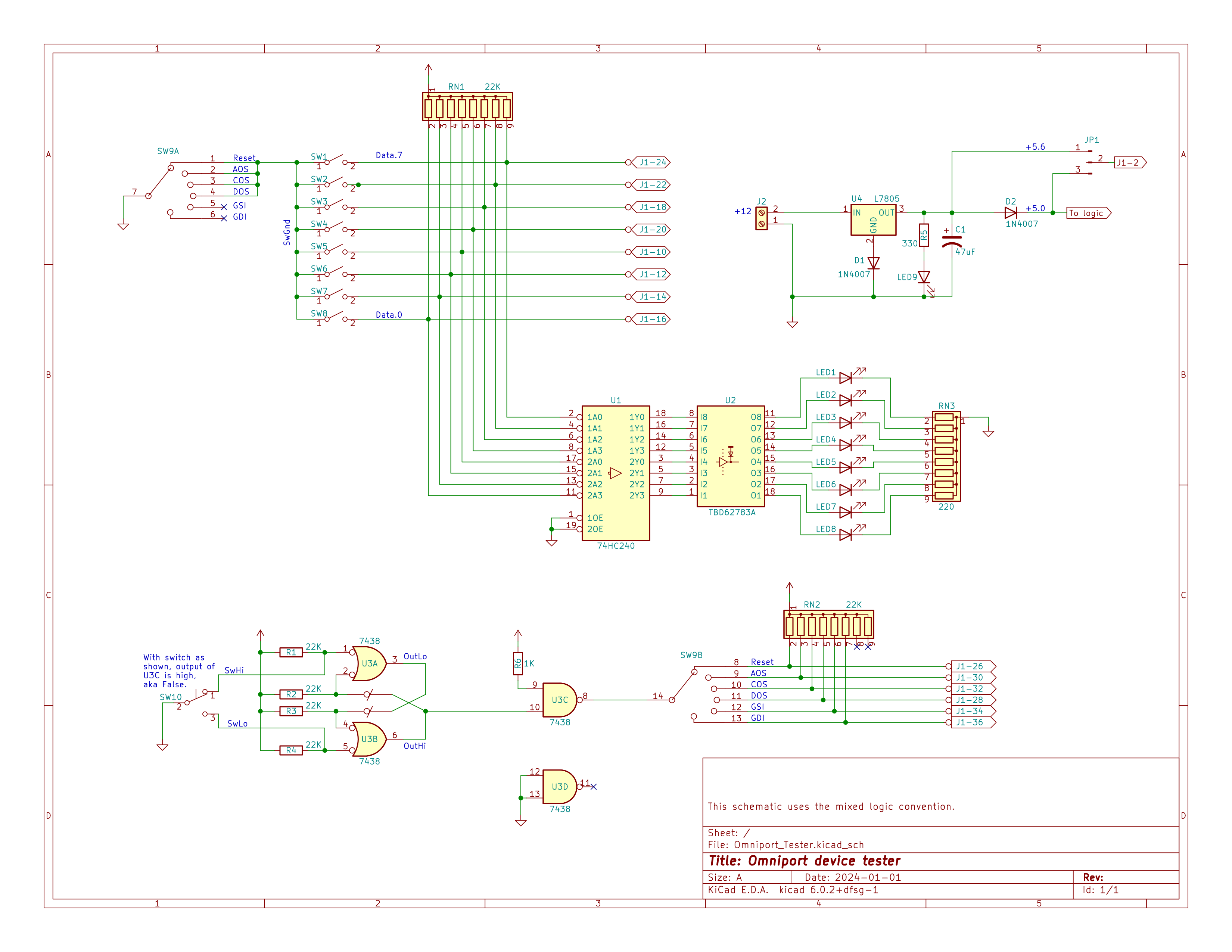
The OmniTester is therefor a very simple device which allows a person to manually control the Omniport using switches. The schematic for the OmniTester is thus:
![]()
The signal from switch SW10 is cleaned up by debounce circuitry, just to the right, then - based on the setting of rotary switch SW9 - used to set one of the six Omniport control lines. Those control lines are negative-true so any control lines not set by the switch are pulled False by RN2. The Omniport data lines are buffered and then used to drive the LEDs so the user can see the state of of the data lines. Rotary switch SW9 also enables switches SW1 through SW8 for RESET, AOS, COS, and DOS so for those commands the Omniport data lines are driven by those switches. For GSI and GDI - where the data is coming from the peripheral - those switches are disabled.
At the time when I designed this tester I wasn't sure if the MCM/70 supplied +5 or +5.6 to the Omniport so the tester is configured to be able to supply either, jumper selectable. It turns out that MCM computers supply +5.6 so that it can go through a polarity protection diode thus resulting in +5.0 at the peripheral.
The OmniTester is so simple that I did a modest amount of testing then sent it off to be made into a PCB. In this photo:
![]()
The OmniTester is the device on the left. The white panel with the legends is just thin plastic that floats above the PCB, secured by the switches. The single switch the right of the rotary switch sets the selected control line True or False, while the eight switches to the left set the data to be used. They don't show up in this photo but, on the board, just below each of the eight switches, is the LED that shows the state of the corresponding Omniport data line. In this photo the 40 pin ribbon cable, exiting from the top of the OmniTester, is connected to some breadboards on which is the Rack8 GPI circuitry during early development. The OmniTester was tremendously helpful during GPI development.
-
An Omniport Peripheral - Part 1
12/31/2023 at 01:59 • 0 commentsBackground
We've implemented the Omniport interface, but how do we know it works? We can look at the signals with a scope or a logic analyzer, but the true test is to see if it works with a real live peripheral. Not having any MCM peripherals handy, that means we have to build one.
When it came to peripherals, MCM sold various kinds - a daisy wheel printer, a dual floppy disk drive, an RS-232 interface and so on. But they also sold a General Purpose Interface board ("GPI board" to it's friends) which interested customers could use as the basis for an interfaces to any device of their choice. The GPI board looked after the mundane "housekeeping" logic of device addressing, device selection and conveniently breaking out various signals. The customer then provided the rest of the interface to their chosen device.
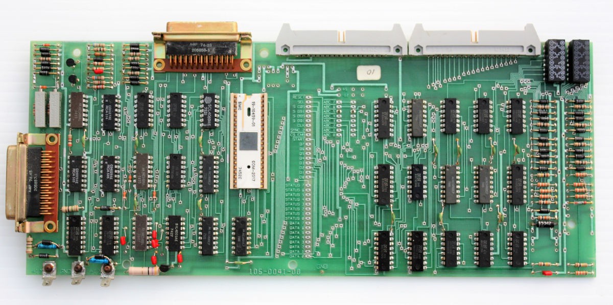
I don't have a photo of an MCM GPI board but, instead, here is a photo of the MCM RS-232 interface which is based on the GPI board:
![]()
The left side of the board is the actual RS-232 interface logic. The right side of the board is pretty much the GPI board verbatim. Which is to say that when it came time to create the RS-232 interface MCM simply took the GPI board and glued the RS-232 specific logic on the left side. On an actual GPI board the left side was a prototyping area for the users chips.
The vertical row of oblong pads down the middle of the board is where the GPI section of the board provides the broken out signals.
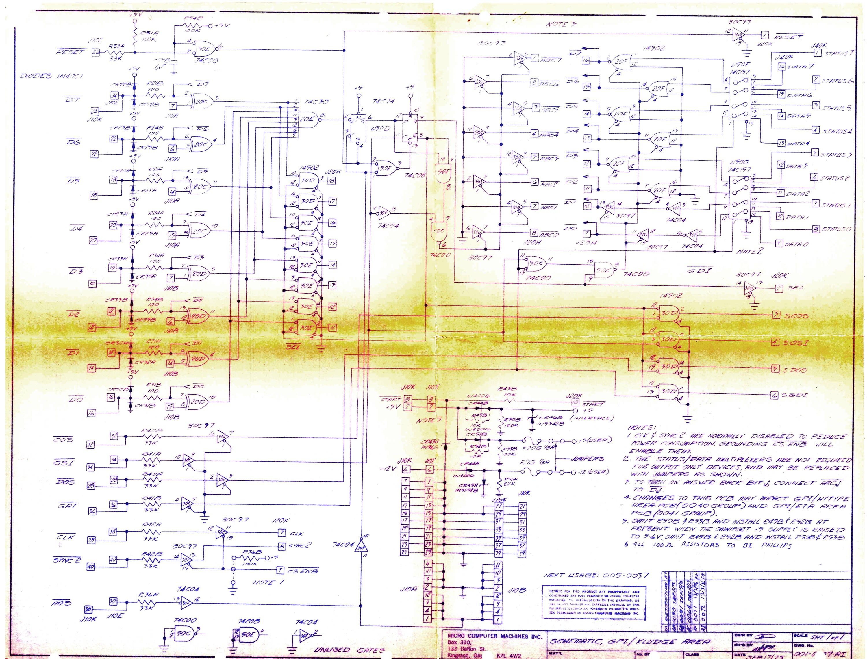
The one and only MCM schematic diagram that I happened to have is of the GPI board, dated 1975, here:
![]()
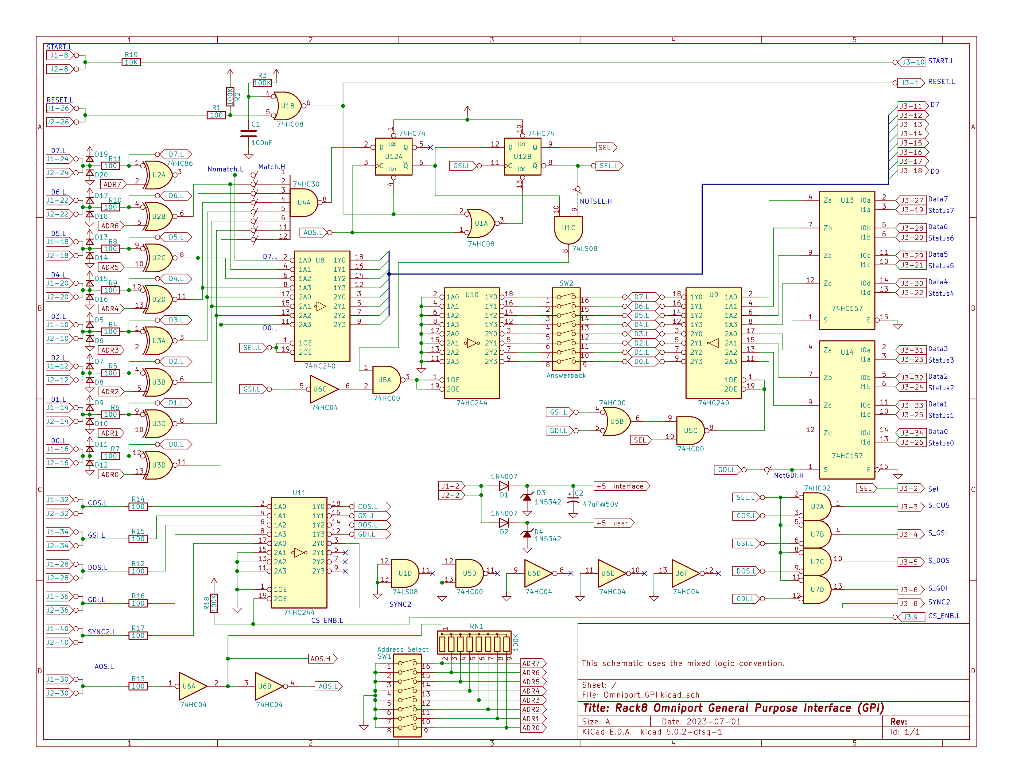
In aid of keeping power consumption down it's all CMOS chips but given that this was in the relatively early days of CMOS some of the chips are unavailable and for others there are now better choices. I did a pretty literal transliteration of the MCM schematic,mutatis mutandis, and came up with this schematic for the Rack8 project's version of a GPI board.
![]()
The omniport lines from the computer come in on the left, while the various lines to and from the users interface are on the right.
How the Omniport works
An MCM document "STANDARD OMNIPORT INTERFACE - Preliminary System Documentation" is HERE.
Each Omniport device has an address. Addresses can range from 1 to 255; address zero is reserved for the keyboard/selfscan device. On the Rack8 GPI board, above, the device address is set by DIP switch SW1. The MCM/70 computer selects a particular device by putting the address of the device on the Omniport data lines and then pulsing the Address Out Strobe (AOS) line. This deselects all connected devices, and puts the addressed device in what we might call the "preselected state". The Gate Status In (GSI) line is normally used to fetch a byte of status information from the device but, for the pre-selected device, the first GSI following an AOS returns the Answer Back Code (ABC) of the device. At that point the device is now fully selected. On Rack8 GPI board the answer back is set by DIP switch SW2.
The Answer Back Code is an 8-bit value which supplies some information about the peripheral. The X'80' bit is true for devices that can do input. The X'40' bit is true for devices that can do output. The X'20' bit is true if the device is interactive (i.e a terminal) while the remaining five bits are a code which identifies the particular device. Some known MCM device codes:
- 0 - EIA/ASCII terminal
- 1 - MCM cassette drive
- 2 - MCM/Hytype daily wheel printer
To send a command to the peripheral the MCM/70 puts the command bits on the Omniport data bus then pulses the Command Out Strobe (COS) line.
To send a data byte to the peripheral the MCM/70 puts the data bits on the Omniport data bus then pulses the Data Out Strobe (DOS) line.
To read the status byte the MCM/70 pulses the Gate Status In (GSI) line which prompt the peripheral to put its status information on the Omniport data lines.
To read the data byte the MCM/70 pulses the Gate Data In (GDI) line which prompts the peripheral to put it data information on the Omniport data lines.
And finally there is the Reset line which, when pulsed, tells all peripherals to reset themselves to their default state.
-
I/O - Part 2
11/13/2023 at 19:03 • 0 commentsMost of the I/O for this machine was covered in the previous log. Next up is the Omniport and the system latches.
The Omniport
The Omniport is the 8-bit bidirectional bus that MCM computers use to talk to their peripherals - printers, disk drives, RS232 interfaces and so on. There are eight data bits and six control bits. In operation, the MCM computer is always in full control of the Omniport and the peripherals simply respond to commands from the computer; the peripherals never initiate anything in terms of what happens on the Omniport.
The logic to implement the Omniport is pretty straightforward and is shown HERE. All the signals on the Omniport are active low. When nothing is happening on the data portion of the bus resistor network RN10 keeps the data lines high, that is, idle. U44, the GAL at the top of the diagram, orchestrates things; you can see the equations for the GAL HERE. When it's time for the CPU to send data to the Omniport the data is latched at U48 and U47 is enabled. U47 is open collector so it can pull low but it can't source. Thus all lines are pulled high by RN10 except for those pulled low by U47. When it comes time for the CPU to read data from the Omniport, U49 is enabled which gates data from the Omniport onto the data bus.
So the logic is straightforward, but getting the correct timing for the control signals was not. I was fortunate to have a copy of the Omniport specification, a relic of my days at MCM, so I knew what was required. GAL U44 looks after the generation of the control signals. To do this it users the GATE0 and GATE1 signals which come from GAL U38 and D-flip-flops U45 both of which are on the main I/O schematic HERE. There are two types of control signals:
AOS (address out strobe), COS (command out strobe) and DOS (data out strobe) put data on the Omniport for use by the peripheral. GSI (gate status in) and GDI (gate data in) read data placed on the Omniport by the peripheral. These control signals are the result of I/O instructions executed by the code.
The System Latches
The MCM/70 CPU needed to be able to receive a signal from the power supply saying that AC power had failed and it was now running from the battery, which was six "D-cell size" lead-acid cells. The machine was power hungry enough that the battery would keep it running long enough to save the content of RAM to tape, but not more. In addition the CPU needed to be able to send a signal to the power supply telling it to shut off. Thus on Rack8 there is an 8-bit input latch (U50) and an 8-bit output latch (U51), both on the main I/O schematic HERE.
-
I/O - Part 1
05/02/2023 at 23:34 • 0 commentsThere is a fair bit to the I/O side of this machine. I had planned on doing a log entry once the I/O was done but it's taking a while so let's do an update now.
There are six facilities to the Rack8 machine's I/O:
- The Keyboard
- The Bank Latch
- The Memory Mode Latch
- The Debug Latches
- The Omniport
- The System Latch
Currently the first four are up and working while the Omniport and the System Latch are next in line for implementation. So what are these things, and what are they for?
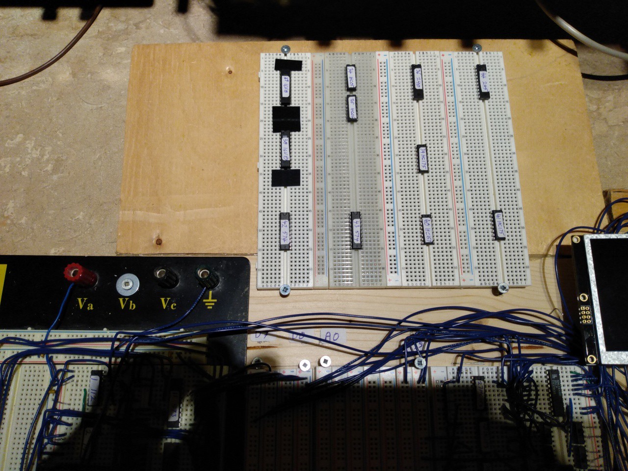
But before we launch into the details, a couple of photos. The breadboard version of Rack8 is built on a piece of wood to which are attached the solderless breadboards. But the board was full and now it was time to implement I/O. So I literally glued another piece of wood onto the top of the existing wood, attached more solderless breadboards, and populated it with the proposed I/O chips. Photo, as of two weeks ago, here:
![]()
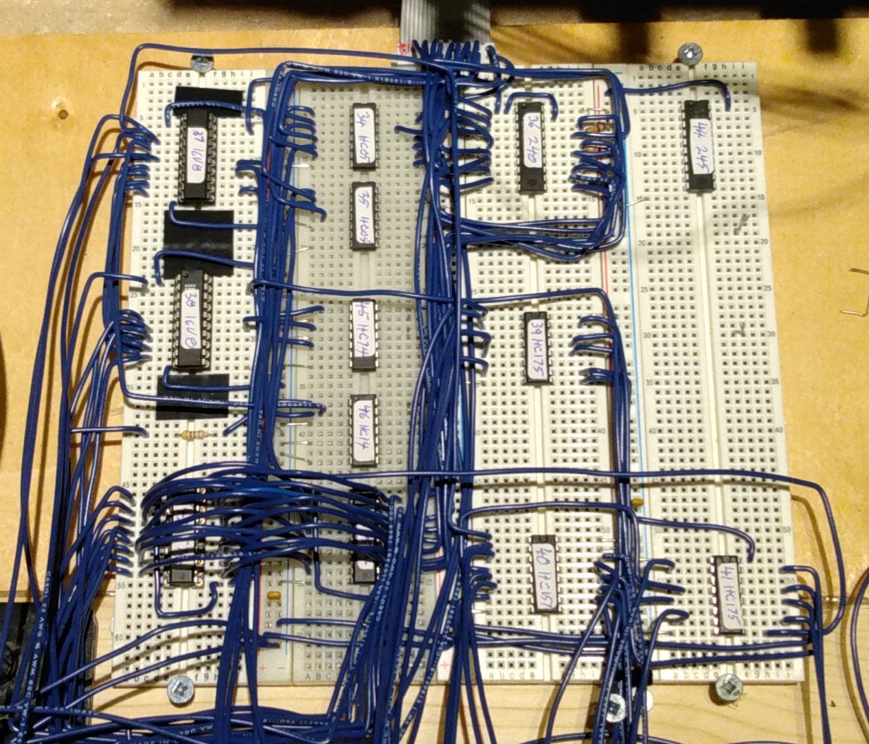
Now with much of the I/O working it looks like this:
![]()
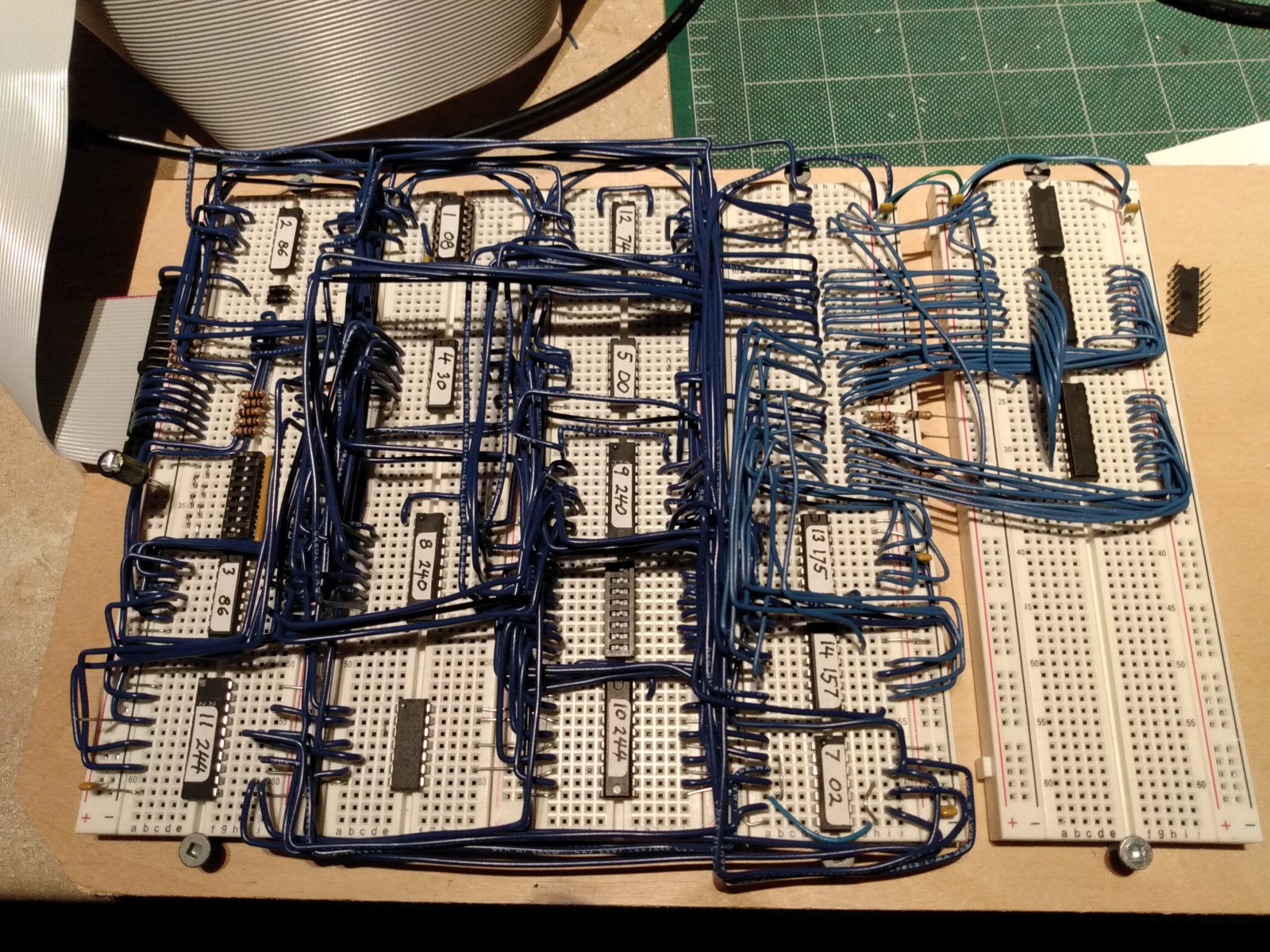
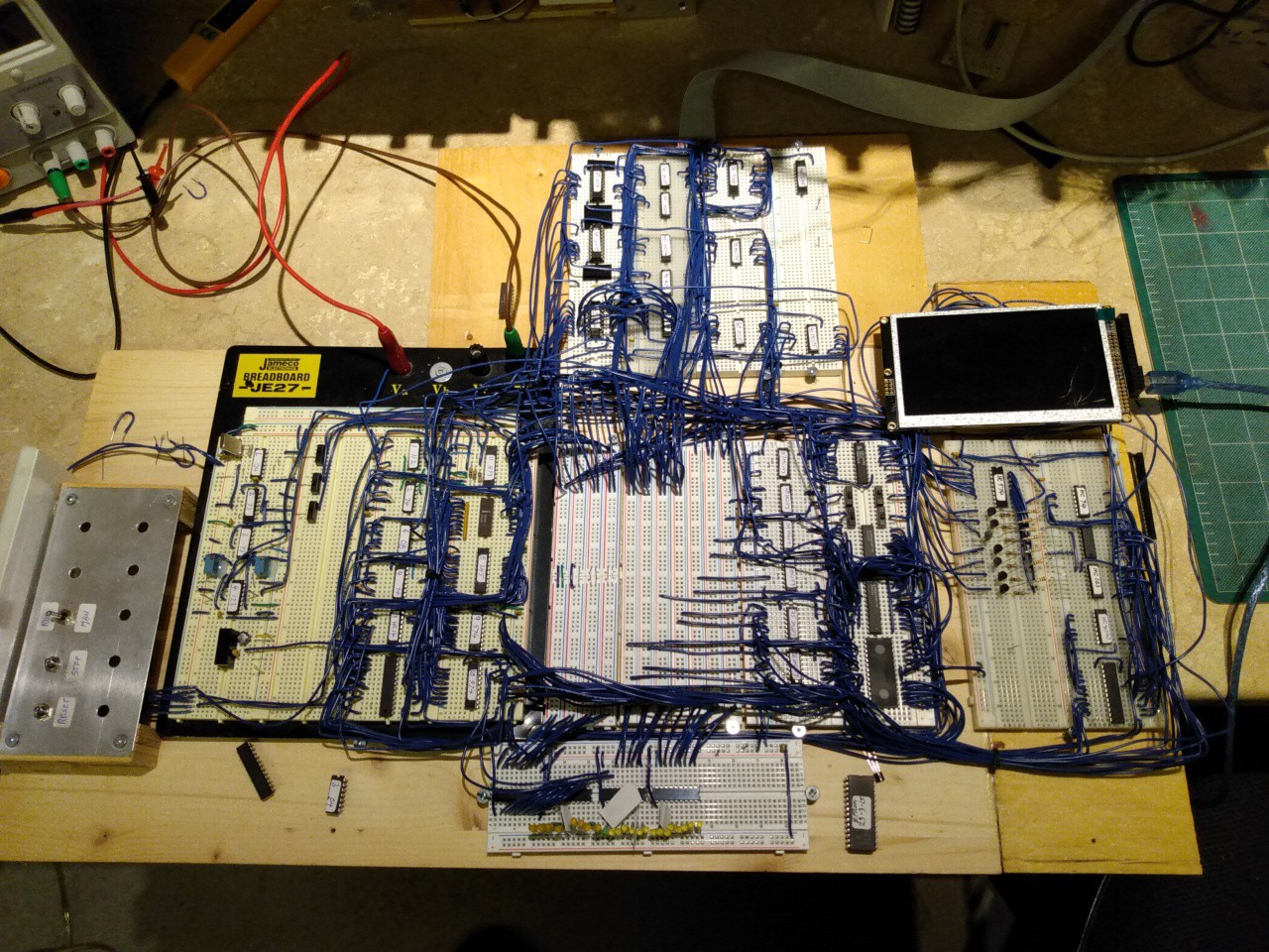
while the whole project now looks like this:
![]()
with the I/O section way up at the top. Note the 20 conductor ribbon cable at the very top which goes off to the keyboard.
The schematic for the implemented-so-far IO can be found here.
Behind The Scenes...
There are two GAL chips, upper left corner in the schematic, that generate the pulses to clock the various IO devices and any other signals needed. The logic equations for those GALs can be found here and here.
The Keyboard
It's kind of obvious what this is for but the way it is implemented in the MCM/70 and hence this machine is interesting. Unlike most microprocessors, the 8008 I/O-READ instruction is actually a WRITE-READ operation. Yup, a single instruction can both write and read at the same time. During a READ operation the content of the accumulator is presented on the low 8 bits of the address bus while the data to the processor you need to present on the data bus.
The MCM/70 took advantage of this when reading the keyboard. The keyboard itself is just an X-Y matrix of keys; no chips, no diodes, just the keys. To scan the keyboard the CPU does an IO-READ operation wherein - on the WRITE side of things - it sends one bit to the X part of the matrix and - on the READ side of things - sees what comes out from the Y part of the matrix. By probing all eight possible WRITE bits you can which key is down, or if none are down.
In the schematic the components for the keyboard start in the middle and then move diagonally to the upper right. In the middle U34 and U34 - open drain inverters - send the bits from the address bus to the keyboard which is connected to J5. What comes back from the keyboard is gated onto the data bus by U36. Because it's driven open drain, the pullup resistors RN5 keep any undriven lines high. Part of the reason that it's driven open drain is that the keyboard, like the original MCM keyboard, has no diodes so open drain keeps things from shorting if the user presses more than one key at a time.
The Bank Latch
Like the MCM/70, this machine has 16 banks of 2K each at address X'1800'-X'1FFF', and only one bank at a time can be active. A 4-bit latch, set by IO write instruction X'51', selects the current bank. In the schematic the Bank Latch is over on the right side in the middle. Nothing exciting here although - brain fade alert - I initially had the input to the bank latch connected to the data bus. You get data from the data bus, right? Well not on this machine you don't. Took me a bit of debugging to figure that out, then we had a DUH moment, followed by some rewiring. Then it worked..
The Memory Mode Latch
As discussed in the Real Memory log post, there are four bits that control the mode in which the Rack8 memory works at any given time. In the schematic U41 is the 4-bit latch that actually provides the bits. When the machine is running, the memory mode can be changed by issuing an X'59' I/O instruction. In that case, the data for the latch comes from the address bus via U40, a quad 2-to-1 multiplexer. But when the machine is reset, then the mux supplies the bits from four switches, so that the machine can be placed in a known memory mode at reset time. The PINT signal ("processing interrupt") is high when an interrupt, aka reset, is in progress which tells to mux to supply data from the switches.
The Debug Latches
On the original rack machine we had a software debugger which allowed us to set breakpoints, to view and change registers and memory, and to trace instructions one at a time. In order to do that the debugger had to be able to save and restore the state of the machine. But, unlike later microprocessors, the 8008 is incapable of saving its own state. In particular you need to save the registers. The obvious place to save the registers is in memory. But in order to store a byte in memory you have to load the H and L registers with the address of the memory, in the process wiping out the values in the H and L registers. Fabulous. So to solve this problem, the debug latches are a pair of one-byte registers which can be written and read using an I/O instruction. Fortunately I/O instructions don't alter the condition codes.
Note that the debug latches, like the keyboard, make use of the WRITE-READ capability of the 8008 READ instruction. When clocked, the old value is presented to the data bus while the new value is captured from the address bus. It's quite handy.
Thus, to save the state of the machine, the drill is:
- Read debug latch 0. That puts the value from the A register into debug latch 0, thus freeing up the A register. It also gets you the value that was previously in debug latch 0 but right now we don't care about that.
- Copy register L to register A and sent it to debug latch 1.
- Copy register H to register A.
- Load the address of the register save are into H and L then save the registers.
Next you need to save the condition code. The 8008 also has no good way of getting those so you just do various tests and note the results. Technically the condition codes are output on the data bus during the T4 cycle of memory cycle two of an IO read but doing anything with that would involve yet more hardware; a bit of software is rather less work.
On the schematic the debug latches are on the left, just under the GALs.
Restoring the state of the machine is pretty much the reverse of the above. The 8008 has no way of restoring the condition codes directly; instead, based on what you want them to be, you need to do some fancy dancing in software but it is possible.
The Omniport - implementation in progress
The omniport is the bidirectional I/O bus by which all external peripherals (e.g. printer, floppy disk, card reader, RS232 interface etc.) communicate with the MCM/70.
The System Latch - implementation in progress
The MCM/70 needed to be able to receive and send a few bits of "system" information. In particular it received a signal from the power supply saying if mains power had been lost. In that case, the machine would if possible save the content of memory to cassette tape and then do an orderly shut down. It was like "suspend to disk" long before that became a popular option. It also needed to be able send a signal to the power supply telling it to shut off.
-
The Keyboard - Part 2
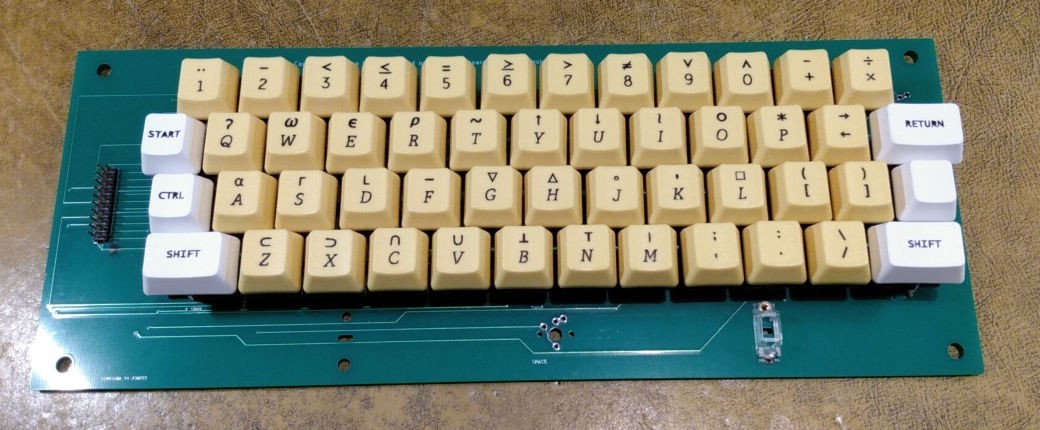
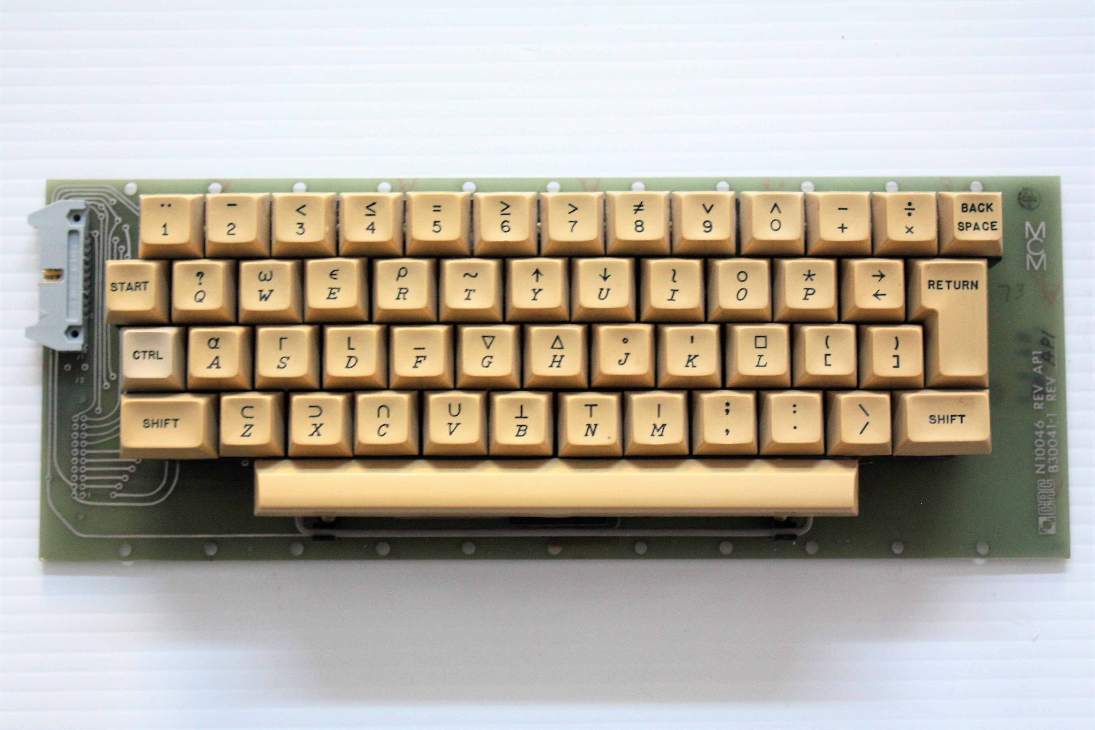
05/02/2023 at 23:20 • 0 commentsI've spent the last few weeks working on I/O but the keyboard is one of the main I/O devices so it kind of fell into the mix. The good news is that the keyboard itself works as intended: no messed up traces on the PCB or the like. The bad news, not that there was much bad news, is that I was short a couple of key switches and had to order more. There is not much more to say about the keyboard beyond that it works and I think it looks great. The keyboard, less the missing Space and Backspace switches, looks like this:
![]()
While an actual MCM/70 keyboard looks like this:
![]()
Not identical, but close enough.
-
The Simulated SelfScan
03/23/2023 at 20:01 • 0 commentsI don't have a SelfScan. eBay doesn't have any SelfScans. I would be delighted to source a working SelfScan and, in theory, it should plug into my Rack8 machine and work, provided I conjured up the required +250 Volt supply. If I had a real SelfScan I would be willing to do that. But in the mean time I've built a Simulated SelfScan which is plug-compatible with a real SelfScan other than not needing the high voltage.
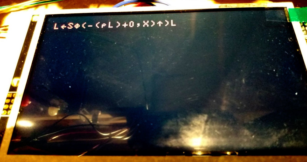
So here is my simulated SelfScan showing a few of the special APL characters (and a Syntax error, but we will overlook that):
![]()
The photo really doesn't do it justice The crud at the bottom is reflections off the screen (which the camera picks up like crazy but in person is hardly noticeable) and the actual text is much closer to "SelfScan orange" than the photo would suggest. My simulated SelfScan consists of:
- An Arduino Mega which responds to the Clock, Reset and Data lines that are intended for a real SelfScan, and
- A 5" LCD TFT 480 x 272 color display screen from buydisplay.com. By using four screen pixels for each SelfScan pixel we use up 444 of the available 480 pixels in width.
The displayed line is smaller than what a real SelfScan would show but it's way bigger than the usual text on my laptop so it's easily readable. A 7" display would probably result in something close to original SelfScan size.
In the photo above it is the 8008-1 CPU, and the SelfScan interface described in the previous log, doing all the work. All the Arduino is doing is pretending to be a SelfScan. If I ever do get a real SelfScan, that would be great, but for now this will do.
The code currently in the Arduino is proof-of-concept and quite slow: it takes about one second to do a full update of the SelfScan line. But we are turning on each LCD pixel individually and there are 6216 of them. There are various techniques that will speed this up a lot. Now that I know it works, writing that code is worthwhile.
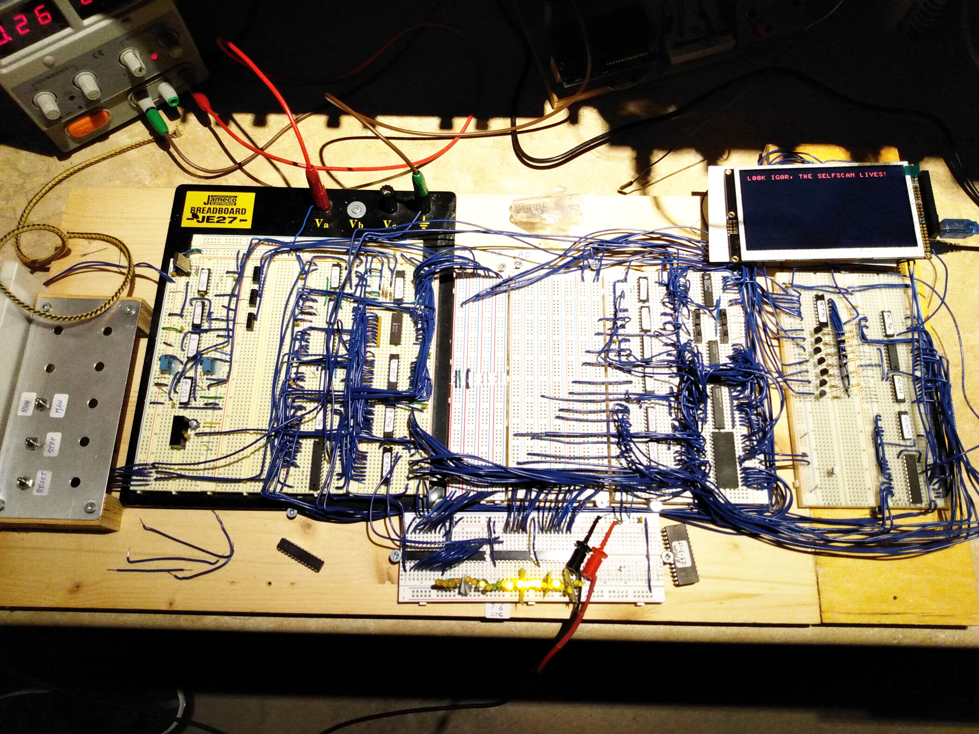
The entire system, as it currently stands looks like this:
![]()
The simulated SelfScan is upper right with the SelfScan interface just below. There is actual text on the SelfScan but you will probably need the larger image to make it out.
-
The SelfScan Interface
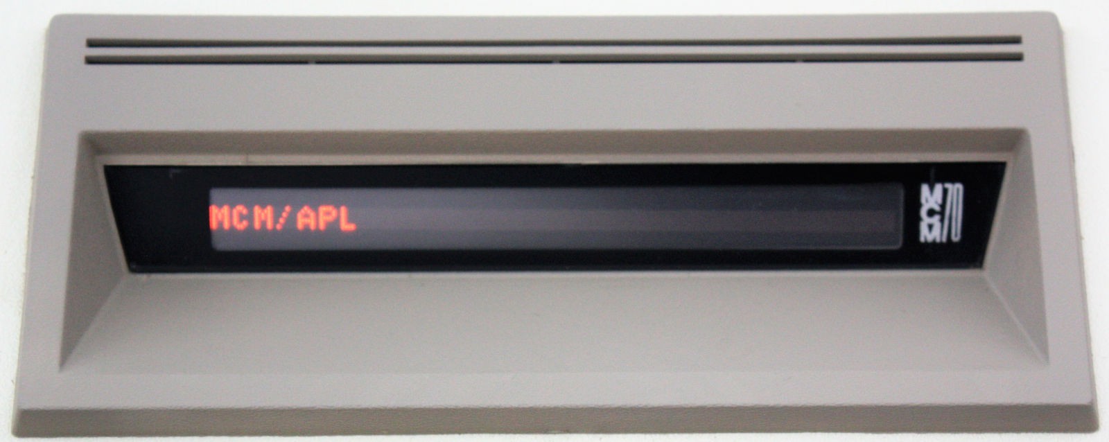
03/23/2023 at 00:16 • 0 commentsThe SelfScan was the visual output device for the MCM/70 computer. It could display one line of 32 characters, and it looked like this:
![]()
CRTs were available at the time but they were very big, very heavy and very expensive. Not great for what was intended to be a small, portable machine. The SelfScan, made by Burroughs, was a plasma display device with the method of operation similar in some respects to a Nixie tube. It was called a "self scan" because you didn't have to address the dots on the screen: after hitting it with a Reset pulse you then provided the 222 bytes of data in order and it "scanned" along by itself. It was actually pretty clever. Today it looks horribly dated but in the early 1970's it was quite reasonable. The version used by MCM provided a screen 222 pixels wide by 7 pixels high. Being memory mapped it allowed MCM to display all the special characters used by the APL language. You can see a scan of the SelfScan data sheet here (PDF). That sheet references a smaller model of 111 columns but the rest are the same.
In terms of interfacing, it is both:
- Simple: Only nine signals: Clock, Reset and 7 data lines.
- Fussy: Needs +250 volts, the clock is asymmetrical with specified high and low times, data has to be provided at precise intervals, you have to make sure you let go of the data lines during reset and for the first 15uS of each clock pulse, and you must be able to drive the data input pullups down to no more than 300 milliVolts.
And you have to implement this memory mapped device with a CPU that has no idea what DMA is.
The Interface Design
The schematic for the Rack8 SelfScan interface is here (PDF), while the logic for the 22V10 GAL is here. Looking at the schematic now it seems all very obvious. When I started working on the design it wasn't the least bit obvious. There were many iterations of trial and error, mostly error, before I arrived at the current, working, version. Fortunately most of the error was on paper - oops wrong edge, oops that's a clock too soon, oops the signal we need is now gone, oops that output needs to be clocked, oops we have no output to clear that flip-flop etc. etc. etc. Possibly because I am more of a software than hardware guy. But eventually I came up with the current design. Even then there was some debugging to be done at which time my old Bitscope was a life saver. I'll have to do a post on the Bitscope. The thing is at once tremendously useful but also tremendously frustrating.
Here be a photo of the working SelfScan interface:
![]()
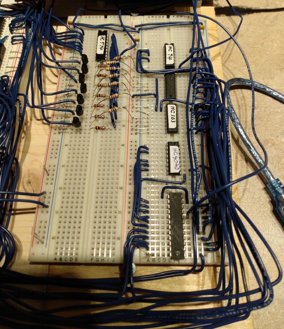
Counterclockwise from bottom right: the 22V10 GAL, the 74HC4040 Sync Counter, the two 74HC163 counters that generate the low 8 bits of the memory addres, the 74HC74 flip-flops, the 74HC573 data latch and finally the seven MOSFET transistors. Only six chips and a handful of transistors but it was a tricky design.
How it Works
Let's start with U19, the Sync Counter. It is a 74HC4040 12-bit ripple counter although in this application only the low 6 bits are used. It is clocked by the SYNC pulse from the CPU which is chugging along at 400KHz or 2.5uS per cycle. The clock is negative true so we use SYNC.H as the clock.
This Sync Counter is used as a time base to make sure that things happen when they are supposed to. In particular, to keep the SelfScan happy we need to:
- Clock it with a signal which is high for 115uS and low for 25uS.
- Issue a negative-true Reset pulse which is True for one clock period.
- After the Reset pulse is over, present data on the data inputs which have pullups and must be driven open-collector or open-drain.
- The data inputs must be left to float high during the entire reset pulse and for the first 15uS of each clock period.
So the low 6 bits of the Sync Counter are fed to the GAL. When the Sync Counter gets to 56 it is reset by the GAL. 56 x 2.5uS = 140uS which gives us the correct period for the SelfScan Clock.
For the first 10 counts, aka 25uS, the GAL makes the clock to the SelfScan low, for the rest of the time it is high. Bingo we have the clock for the SelfScan.
It is worth noting that the 74HC4040 is a ripple counter so you have to be careful to ignore the outputs just after it has been clocked. Toward that end, the GAL develops a clock for itself - based on SYNC from the CPU - which is guaranteed to be at a safe time. That clock comes out on pin 23 and is fed to pin 1 of the GAL to be used to clock those registered outputs that need to be careful.
Next up are U22 and U23, both 74HC163 synchronous binary counters which form the SelfScan Address Counter aka SSAC. They are clocked once per SelfScan clock. Probably best to explain how they work by starting at the end and then working forward. When the SSAC reaches FF it set it's RCO (ripple carry output) signal True. U3f inverts this and applies it to the LOAD.L inputs of the SSAC. At the next clock pulse X'21' (which is hard wired on the data inputs) is loaded into the SSAC. Why X'21'? Well the RAM area for the SelfScan starts at X'2022'. The memory system provides the high byte of the address while the SSAC provides the low byte. It is X'21', not X'22', because while the SSAC is at X'21' the Reset pulse is being applied to the SelfScan and during reset the address does not matter. So on the next SelfScan clock pulse after Reset the SSAC will be at X'22' and we will then present the data from memory address X'2022' to the SelfScan for the first column of data.
But we need to generate the Reset pulse to the SelfScan and we need to generate it after the cycle where the SSAC is X'FF' is over. Thus we feed the RAC.L signal to U21A, the "RCO catcher flip-flop" which is clocked by the SelfScan clock line. When the GAL sees the output of the RCO catcher go true it know it's time to to start a reset pulse to the SelfScan. Then U21b comes into play. It is nominally a D flip-flop but here we are using it as a simple set/reset flip-flop. We set it to initiate the Reset pulse to the SelfScan and we clear it when the pulse is done.
Now there is the matter of getting data from the memory to the SelfScan. For memory mapped devices you might normally use DMA but the 8008 CPU has no clue about DMA. Instead we use what might be called SMA: Stealth Memory Access. Basically we access memory for the SelfScan when the CPU isn't looking. When the CPU is halted, or waiting (ie during single stepping) then the address and data busses are free and we can use them with impunity. When the CPU is executing instructions we have to be more careful. Every 8008 CPU instruction starts with T1 and T2 cycles, when the CPU is outputting he high and low portions of the address. Then on the T3 cycle it actually accesses memory. But during T1 and T2 the address and data bus are unused by the CPU. Thus during the T1 cycle we issue a pulse on the READ_SS.L line to memory which accesses RAM and puts the data from X'20xx' on the data bus, where xx comes from the SSAC. U18, our SelfScan Data Latch, receives the data from the data bus when clocked by the GAL. The GAL needs to know when the CPU is halted, waiting or doing a T1 thus we run the S0, S1, and S2 lines from the CPU into the GAL.
The Selfscan Data Latch is tri-state. When enabled, it drives the transistors Q1 through Q6 which in turn drive the SelfScan data lines. The SelfScan itself has 1.5K pullup resistors on its data inputs so we only have to pull them low; left to their own devices they float high. During SelfScan reset, and for the first 15uS of each SelfScan clock pulse, we have to leave the SelfScan data inputs alone to float high. We do this by disabling the SelfScan Data Latch outputs at which point RN3, a bunch of 22K resistors, pulls the gate of the MOSFETs low thus turning them off and allowing the SelfScan data lines to float high. We use MOSFETs because, when active, we need to be able to pull those lines down to no more than 300mV (per the SelfScan data sheet). There were other possibilities but it's always fun to have at least a few discrete transistors in play. And it works.
Rack8 MCM/70 rack machine replica
Goal: Build a replica, using an actual 8008-1 chip, of the "rack" machine used at Micro Computer Machines when developing the MCM/70.
