-
Real Memory
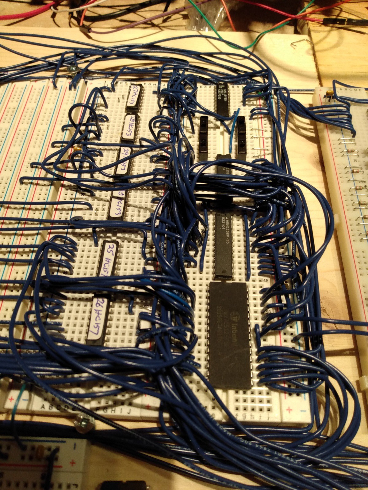
03/22/2023 at 15:01 • 0 commentsHere is a photo of the working Real Memory:
![]()
Foreground right the 64Kx8 EEPROM. Above that the two 64Kx4 RAM chips (the upper one partially obscured by the wires). Above that the four switches which are standing in for the memory mode flip-flops. And above that, the 16V8 GAL. On the left are the six multiplexer chips.
On to the design
With the keyboard PCB in hand, if not yet assembled, it was time to move on to Real Memory. But first we need to talk a bit about the memory layout of the MCM/70 production machine, the memory layout of the original MCM rack machine, and about the proposed memory layout for my Rack8 machine.
The address space in the production MCM/70 is laid out thus:
- X'2000' - X'3FFF' - 8K RAM - the workspace for the user.
- X'1800' - X'1FFF' - 16 ROM banks of 2K each, only one of which can be active at a time.
- X'0000' - X'17FF' - 6K ROM of frequently used routines.
The MCM rack machine, which was intended for program development, had a similar layout except that most of the ROM mentioned above was replaced by RAM. Only the lowest 2K - X'0000' through X'07FF' was EPROM in order to have some code when the machine was reset.For the Rack8 machine clearly we want to have RAM where the MCM rack machine had RAM and EPROM where the MCM rack machine had EPROM. But wait! There's more! In addition to working like the old MCM rack machine I would like the Rack8 to be able to run MCM/APL by flipping a switch. So, after a lot of cogitation we have the following design criteria:
For the low 2K - X'0000' through X'07FF' nicknamed "LOW" - we want to be able to have:
- A simple loader in EPROM suitable for startup in "Rack" mode, or
- The first 2K of MCM/APL for running APL, or
- RAM for doing development work
For the next 6K - X'0800' through X'1FFF' "nicknamed "MID" - which includes the bank area we want to be able to have:
- MCM/APL in EPROM, or
- RAM for development
And the high memory area - X'2000' - X'3FFF' nicknamed "WS" (because it is the users WorkSpace) - is always RAM.
Then what?
So we've got what we want figured out. Now how do we control it? The suggestion is three toggle switches and three flip-flops. The flip-flops will control who gets what in terms of EPROM and RAM, and those flip-flops will be settable by issuing an I/O command so we can change the setup dynamically. The toggle switches will control what the flip-flops get set to when the CPU is reset.
The three flip-flops are:
- LOWRAM.: If True the LOW memory area is RAM, otherwise it is EPROM.
- LOWAPL: Has no effect unless LOWRAM is False. If True then LOW memory has MCM/APL in EPROM, if False then LOW memory has a simple loader in EPROM.
- MIDAPL: If True the MID memory has MCM/APL in EPROM, if False them MID memory is RAM.
Note that if all three switches are False then we have something very much like the old MCM rack machine: all RAM except for the low 2K which has the loader and some basic routines.
But wait - there is even more! Flip-flops come in pairs and we are using three so the remaining one is burning a hole in our pocket, so to speak. And in our 64K memory we have a bunch left over. So we invent the flip-flop ALTWS. When True it selects an alternate workspace in RAM. Thus we have, in effect, two workspace banks: the regular one and the alternate one. This is not something that the original rack machine had, and I have no idea what it might be used for, but this is a fun little project so I'm putting it in for fun.
Then how?
So how do we implement this memory scheme? For RAM we are using two M5M5258 64Kx4 chips, and for EPROM we are using one 27C512 64Kx8 chip. For our purposes we consider these chips to consist of 32 chunks of 2K each which we allocate like this:
Address EPROM RAM F800 APL Bank F Bank F F000 APL Bank E Bank E E800 APL Bank D Bank D E000 APL Bank C Bank C D800 APL Bank B Bank B D000 APL Bank A Bank A C800 APL Bank 9 Bank 9 C000 APL Bank 8 Bank 8 B800 APL Bank 7 Bank 7 B000 APL Bank 6 Bank 6 A800 APL Bank 5 Bank 5 A000 APL Bank 4 Bank 4 9800 APL Bank 3 Bank 3 9000 APL Bank 2 Bank 2 8800 APL Bank 1 Bank 1 8000 APL Bank 0 Bank 0 7800 - - 7000 - - 6800 - - 6000 - - 5800 - ALTWS 5000 - ALTWS 4800 - ALTWS 4000 - ALTWS 3800 - WS 3000 - WS 2800 - WS 2000 Loader WS 1800 - MID RAM 1000 APL MID RAM 0800 APL MID RAM 0000 APL LOW RAM In our RAM there is enough unused space that we could have an alternate alternate workspace, but lets not get carried away here. And there is a bunch of unused EPROM but we are using more than 32K so I'm happy enough to leave that as is.
The Gory Details
The schematic of the Real Memory is here (PDF). You can see why I wanted to have the CPU itself and Simple Memory working before I tackled getting this to work. A great deal of what goes on with memory access is orchestrated by the 16V8 GAL, and you can find the logic for it here. Let's go over this a bit at a time.
The Data Bus is dead simple: it comes from the CPU schematic and goes to both the RAM and EPROM. End of story.
The Address Bus is where the fun happens. The CPU has only 14 address bits but our memory chips have 16 bits so, with the aid of some multiplexers and the GAL we develop the Effective Address. We further divide that Effective Address into Low (the low 8 bits), and High (the high 8 bits).
Effective Address Low is the simpler of the two. It always comes from the CPU unless the SelfScan is accessing memory in which case Effective Address Low comes from the SelfScan interface. The SelfScan is soon going to get its own log entry but suffice to say that it is a memory mapped display device which need to get a byte of data from memory every 140uS. If the CPU were doing that it would be so busy servicing the SelfScan that it wouldn't have time for much else. So, yes, we have to use hardware to service the SelfScan. The two 74HC157 muxes, U25 and U26, look after selecting the source for Effective Address Low.
Effective Address High is rather more complicated. There are four mode of access that it needs to deal with:
- Bank (we are accessing memory in the range X'1800' - X'1FFF')
- Loader (we are accessing the loader EPROM)
- SelfScan (we are accessing RAM for the SelfScan)
- Normal (not Bank, Loader, or SelfScan)
For each of our four modes the Effective Address High bits need to be supplied per this table:
Address Bit 00 Bank 01 Normal 10 Loader 11 SelfScan EA15 1 0 0 0 EA14 Banklatch3 ALTWS 0 0 EA13 Banklatch2 A13 1 1 EA12 Banklatch1 A12 0 0 EA11 Banklatch0 A11 0 0 EA10 A10 A10 A10 0 EA9 A9 A9 A9 0 EA8 A8 A8 A8 0 The Effective Address High multiplexers (U27 - U30), under control of the GAL, select the various bits per the above table.
Notes and caveats:
- Banklatch is the four-bit latch, set via an I/O instruction, which says which bank is to be active. No I/O is implemented yet so for now these bits are hard wired to 0 but everything is ready once the real banklatch is working.
- The SelfScan is mapped to memory starting at X'2022' thus, if accessing data for the SelfScan, the Effective Address High is always X'20'. The SelfScan memory is only 222 bytes long so the rest of the Effective Address come on Effective Address Low.
- ALTWS is true if we are accessing the Alternate Workspace; it just moves workspace accesses up into the alternate space.
Sorting all this out is the job of the 16V8 GAL which gets all the inputs shown on the schematic and generates:- A signal to tell the EPROM when to read.
- Signals to tell the RAM when to read and write.
- A signal to the Effective Address Low muxes saying which input to select.
- Two signals to the Effective Address High muxes saying which input to select.
- The ALTWS signal based on the ALTWS flip-flop and other considerations.
And somewhat remarkably, after a very modest bit of debugging, this all works. Next up is the SelfScan interface.
-
The Keyboard - Part 1
03/15/2023 at 16:20 • 0 commentsI wasn't entirely sure what I was going to do for the keyboard, but I got a lot of assistance from friendly folks along the way.
The MCM/70 and the rack machine used an unencoded keyboard - the processor was connected directly to the keyboard and it figured out what key has been pressed by probing the XY matrix of the keyboard. I thought about buying a commercial keyboard and hacking as needed. Then there was the matter of the key caps. The MCM machines ran the APL language exclusively and had key caps showing all the special APL symbols.
From Zbigniew I got a diagram showing the XY matrix layout of the MCM/70 keyboard, but that was just the matrix. It didn't show how the matrix was wired at the connector.
I wanted to make my keyboard pin compatible with the MCM/70 keyboard, so the next task was to figure out that wiring. Santo Nucifora of vintagecomputer.ca has an actual MCM/70 and on his web site has many excellent photos of the MCM/70 including all the PCBs that make it up, including the keyboard. By inspection I was able to figure out about half of the connections, but of course the traces on the one side of the PCB are obscured by the keys themselves. Santo was kind enough - and a big shout-out of thanks here - to take the keyboard out of his MCM/70 and trace out the lines for me. With that in hand I had enough information to design a plug compatible replica.
Then I came across Mike Gardi's MCM/70 Hackaday project. He has made an MCM/70 replica which looks remarkably like an actual MCM/70 while under the hood is running MCM/APL on a raspberry-pi which in turn is running Zbigniew's emulator. It's a very nice piece of work.
Mike, having made replicas of several vintage personal computers, knew where to go to get a custom keyboard and custom keycaps. For the keyboard I was directed to the Unified Retro Keyboard project, the goal of which is to make available open-source designs for retro keyboards. None of the existing retro keyboards (Apple 2, OSI etc) were what I needed but I was able to load the basic retro keyboard design into Kicad, make the necessary modifications, and send it off for production. All with the patient help of Dave, last name unknown, from the Unified Retro Keyboard project. Per Mike's suggestion the actual Futaba keys were ordered from Electronic Surplus. And for the key caps Mike wanted some more and I wanted two sets, one for myself and one for future consideration, so we did a group buy which went well.
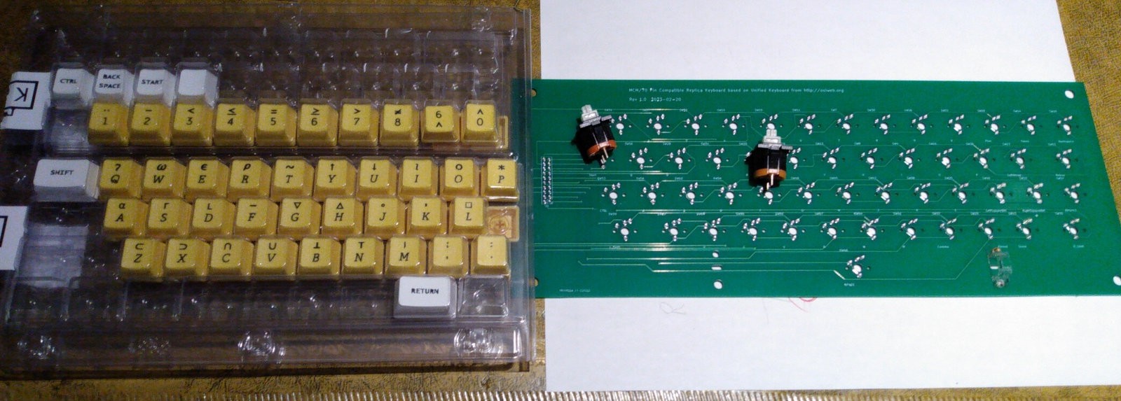
The keyboard isn't assembled yet. There are a great many aspects of this project that need work, and only one person working on it. So the keyboard will have to wait until a few other things are done. Stand by for part-2. The photo below shows the keyboard PCB, a set of MCM style key caps and a two of the Futaba switches.
![]()
-
Goldilocks and the Three Memories
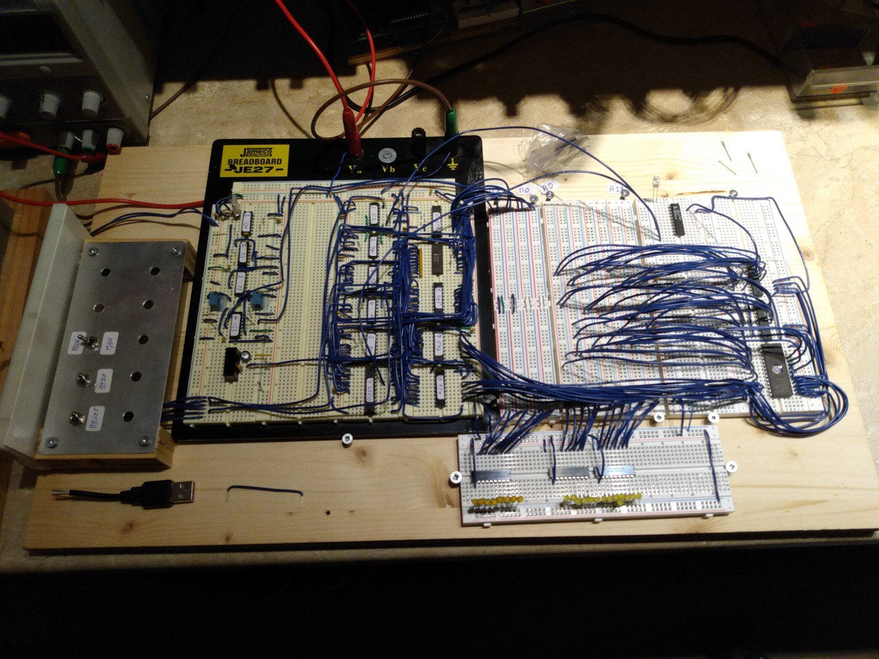
03/12/2023 at 01:33 • 0 commentsOn a couple of solderless breadboards I've build up the CPU and necessary support chips. Then what? Well, we need some memory to test it with but the actual memory layout that I have in mind for the final version is remarkably complex given the 16 banks which can be either EPROM or RAM, the low memory areas which can be either EPROM or RAM and the consideration that the SelfScan interface needs to be able to do what amounts to DMA on the RAM. That's memory number one, and my enthusiasm for debugging that and the CPU itself was, uh, limited.
So let's posit a simple "proof of concept" memory that just has EPROM in the low 8K and RAM in the high 8K. That's memory number two. But for when debugging the CPU what I wanted was something Really Simple. Capital R, capital S.
Therefore we invent "trivial memory". That's just a latch wired up so that whenever the CPU asks to read a byte from memory the latch gates X'C0' onto the bus. X'C0' is a NOP to the 8008. We totally ignore the address bus and we ignore any request to write. With this "memory" in place the CPU simply roars through successive memory locations executing NOPs. That's memory number three. In a sense quite useless but also painfully simple and likely to work, so that's the one I started with.
2023-02-18 Trivial Memory working
Here is a photo of the developments system with the working "trivial memory":
![]()
Left to right:
- Three electrically debounced toggle switches.
- First breadboard panel: the 800 kHz 2-phase clock at the top. At the bottom the +5 to -9 converter. Yes, the 8008 requires +5 and -9. But on the bright side, it requires no ground connection. Seriously, there is no ground pin. Apparently it intuits ground based on +5 and -9.
- One blank breadboard.
- Next two breadboards: CPU and support chips. The 8008-1 CPU, very unobtrusive, is in the right hand row, second from the top.
- Four vertical strips which carry the eight data lines.
- Seven vertical strips which carry the 14 address lines.
- Breadboard with the 2-chip "trivial memory"
- At the bottom, a horizontal breadboard with the LEDs that show the address and data lines, and their corresponding drivers.
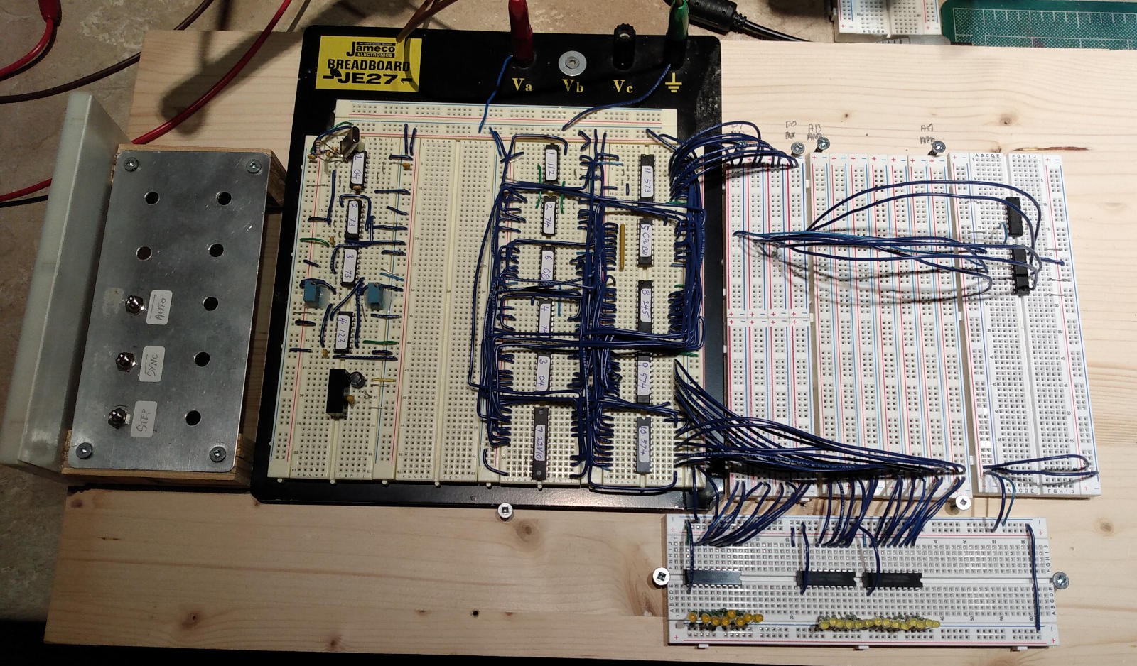
2023-02-27 - Proof-of-concept Memory working
With Trivial Memory working the next step was Simple Memory. The schematic of the Simple Memory is here (PDF) while the logic for the 16V8 GAL is here. It's about as simple as I could make it while having actual memory. A photo here of the CPU and working trivial memory:
![]()
Now over on the right we have a mess of address and data wires. I wasn't too concerned about making these neat and tidy as this memory layout was but a way-station on the way to the real memory. Over on the right is a 64Kx8 EPROM and above that are two 64Kx4 RAM chips. And up above the data+address wires is a 16V8 GAL which supplies the logic glue between the CPU and the memory chips. These memory chips are way more than was is needed for this test, but they are also the chips that I propose to use for the final system, so good to know that they work here.
????-??-?? For-real memory
I've got a preliminary design for the for-real memory, a final design will be forthcoming real-soon-now. But in the meantime I want to get the keyboard looked after - because it will take time to get the PCB produced - and I want to get the SelfScan interface designed because it has to interact with the real memory.
-
The CPU
03/10/2023 at 02:29 • 0 commentsThis project almost didn't get off the ground at all. I've built Z80 systems from scratch, but the Z80 is a dead-easy CPU to make go. The i8008, on the other hand, is not easy at all. It is really about three quarters of a CPU with the rest up to you. It doesn't even have an address bus. What it does have is an 8-bit "everything but the kitchen sink" bus that carries address-high, address-low, control bit, and data. Then it's up to you, the hardware designer, to sort this out into a real address bus based on various status bits. I dabble in hardware but I'm fundamentally a software guy. If I had had to figure out how to make the 8008 go by myself from scratch it probably would have ended there.
Fortunately, as I was looking at starting this project, I came across this web site where Len Bayles had, pretty much as an intellectual exercise, built a time-of-day clock based on an i8008 chip. And even better there was lots of documentation and schematics. His system had significant difference from what I wanted. He had switches so you could toggle data into memory and inspect memory - the original MCM rack machine didn't have that so I don't need it. His machine didn't have the ability to single step instructions, something I want to have. But the guts of his design, looking after all the weirdness to make the i8008 go, was enough to get me off the ground.
He used 74LS whereas I want to use 74HC, and one of the chips he used is no longer available. So there was a certain amount of mutatis mutandis but it was enough of a jump start to get me going.
The 8008-1 requires a 2-phase 800 kHZ clock. The schematic of the current clock circuit is shown here (PDF). I will probably modify this. It's using a 6.4 MHz crystal because I couldn't find any 3.2 MHz or 1.6 MHz crystals at DigiKey. But they do have 3.2786 MHz crystals which I will probably try. I would also prefer to eliminate the one-shots. This was, of course, the very first circuit built for the project and before there was any certainty that the project would go to completion.
The schematic for the CPU section is here (pdf). Clearly much of it is based on Len Bayles clock but with some changes. In the upper left is the circuit that mediates single stepping. The 8008 doesn't really have a single-step feature. What it does have is a READY input that slow memory (the very thought of a memory slower than this 800 kHz processor is somewhat mind boggling, but apparently such things did exist) can set False until the memory is ready, The 8008 marks time until READY is true, and there is no time limit on this. Thus we use the READY line to effect single-stepping, although this has some ramifications for the LEDs that display the address and data lines. Top, center, there is a 74HC574 which can gate one of eight possible instructions onto the data bus at reset time. In Len Bayles clock this was handled by the front panel switches. But Rack8 has no front panel switches, so this function got moved to the CPU. The jumpers at J1 allow any of the 8 "reset" instructions to be used. Once the CPU is up and working it would always be reset-0 but during testing and debugging it is handy to be able to run up to eight different tests.
Rack8 MCM/70 rack machine replica
Goal: Build a replica, using an actual 8008-1 chip, of the "rack" machine used at Micro Computer Machines when developing the MCM/70.