Bharbour
-
A new mounting plate
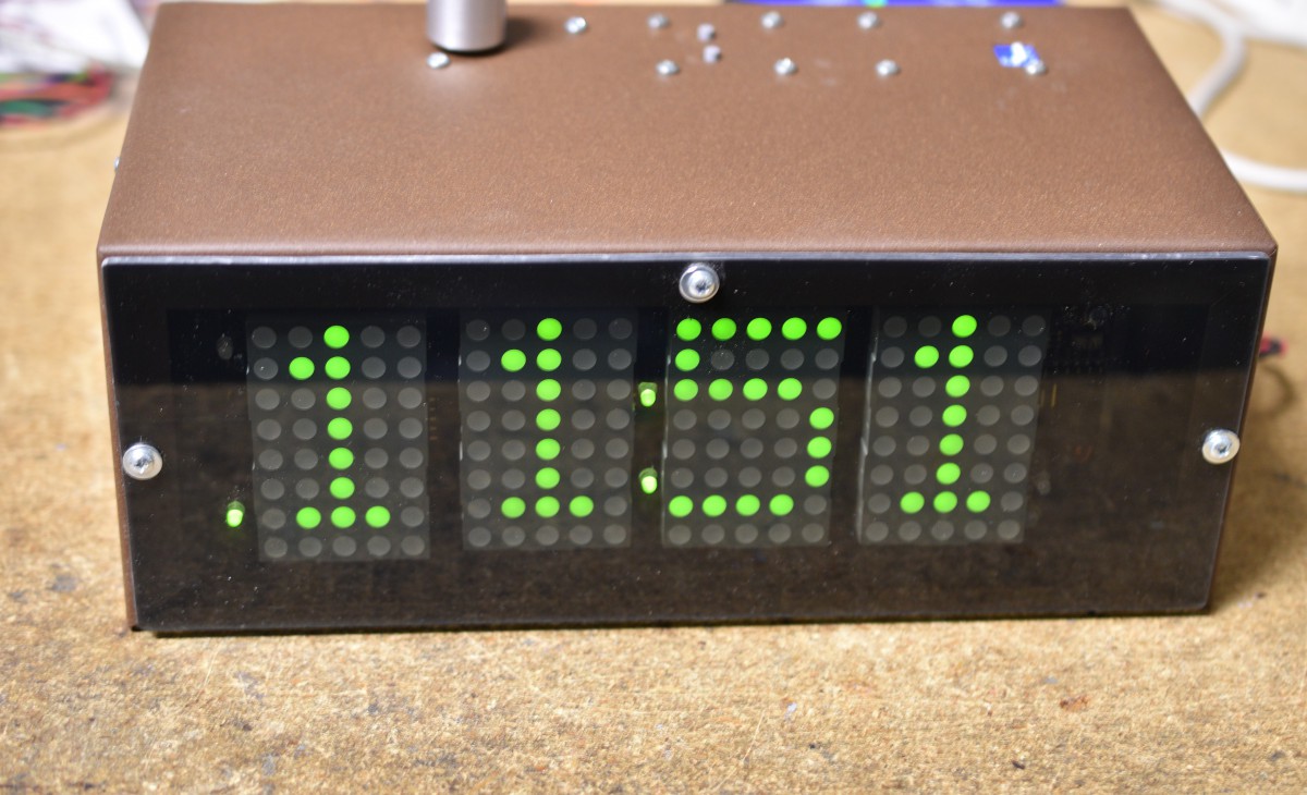
06/11/2023 at 17:34 • 0 commentsAfter using the clock for a few weeks, it became apparent that the gap between the minutes 10 digit and the hours 1 digit was too narrow. The two discrete LEDs that make the colon between the hours and minutes blended into the characters enough that it was difficult to read. Viewing from an angle made it worse. Viewing it at 0 dark thirty, with one eye open and 5 brain cells on line did not help the situation either.
![]()
This is the original layout. If you look at the minute 10s digit, you can see how the colon LED merges into the digit.
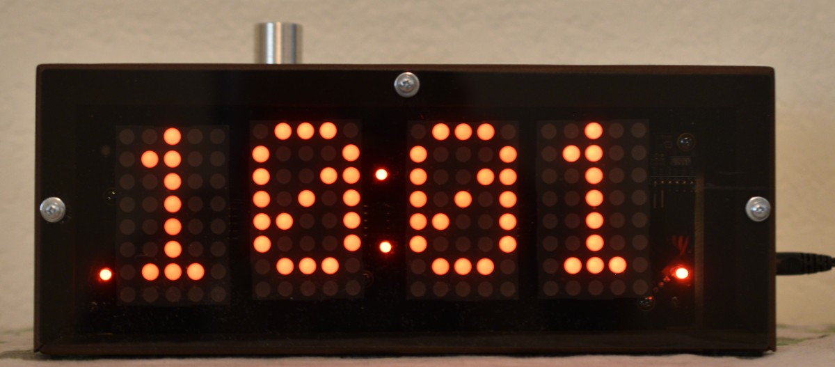
A new mounting plate was made that doubled the distance between the hours and minutes digits. After replacing the mounting plate, It is easier to read.
![]()
The front area around the displays is kind of crowded, but it was possible to move the hours digits to the left and the minutes digits to the right by 0.150" each. It was not necessary to modify the wiring harness to make the changes.
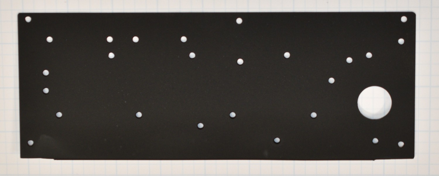
I opted to make a new mounting plate rather than modify the old one. A few changes had already been made to the old plate and the possibility of having the new holes too close to an existing hole seemed likely.
![]()
Here is the new mounting plate. Contrary to the appearance, it was not made with a shotgun :) With components mounted on the front and back side of the plate, you get a lot of holes. The large hole on the lower right side is for wiring to pass through. Originally, the plate was designed in CAD, and it was a pretty simple thing to move the components around and re-dimension the drawing. Drilling was done on a vertical mill with a digital readout, so placing the holes accurately is easy.
-
Top Level Schematic Diagram
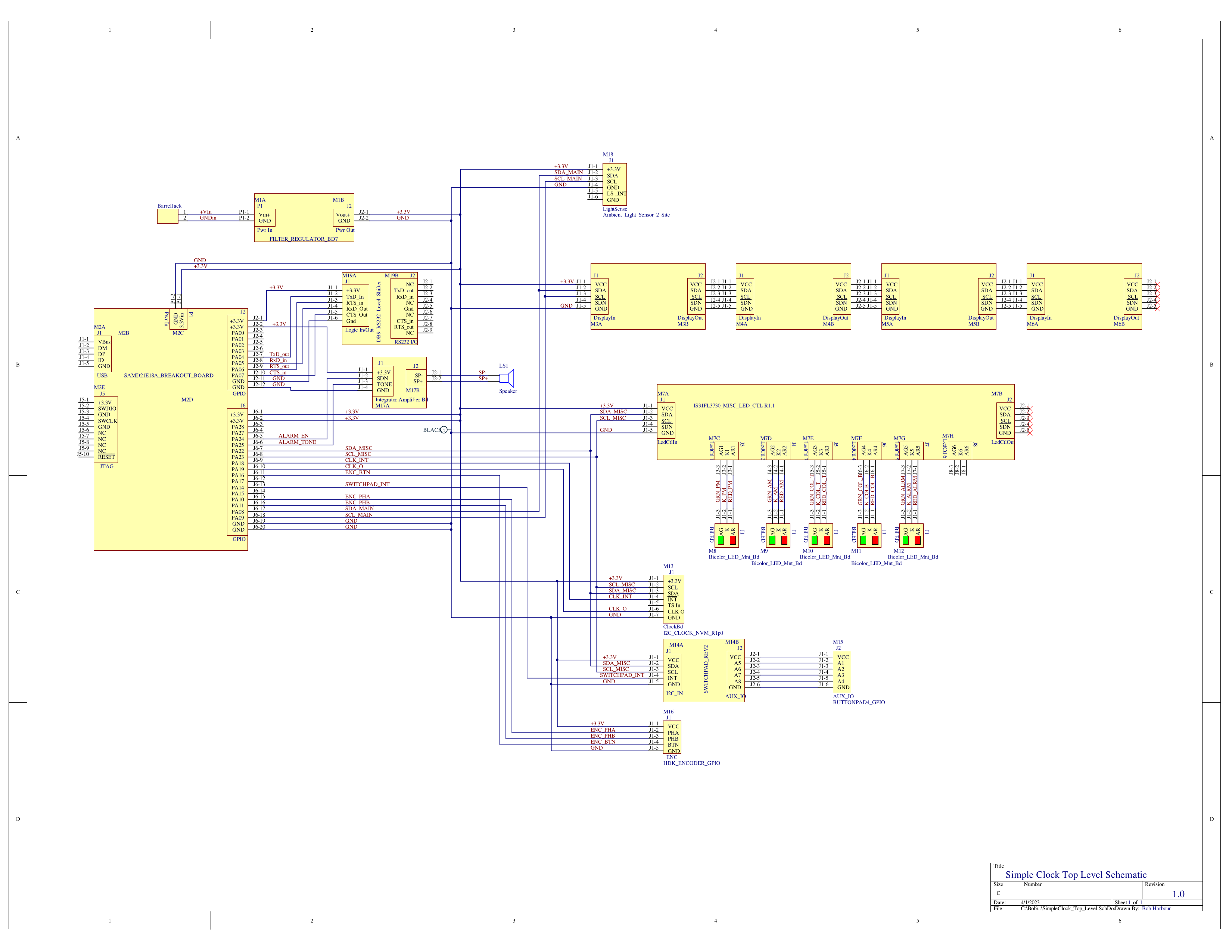
03/19/2023 at 01:51 • 0 commentsHere is the top level schematic diagram, showing the interconnection of all of the individual boards in the project.
![]()
Interconnection is all done with #24 and #22 wire and Molex CGRID ||| connectors. A few years ago, I bought a proper crimper for these connectors, and it has made it easier to build wiring harnesses. The end results look better too.
-
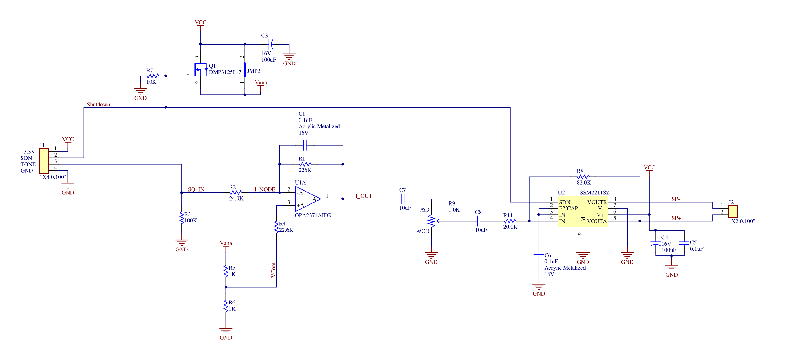
Integrator Amplifier Board
03/19/2023 at 01:46 • 0 commentsThis board accepts a low frequency ( < 1KHz ) square wave from a timer on the MCU,converts it to a triangle wave and amplifies it to drive a speaker.
![]()
When I designed the board, I was not sure how cleanly the integrator would start up when the square wave input begins, so I included hardware to turn off power to the opamp in the integrator. The first board got built with Q1 not populated and JMP2 populated, which leaves the integrator powered all the time. With a little testing, it looks like the integrator starts up cleanly and the output voltage moves down to be centered around the 50% VCC point within a few cycles. The Integrator output is AC coupled to the volume control R9, so there is no DC current as a result of the integrator output sitting at 1.8V.
Similarly, the input to the speaker driver chip U2 is AC coupled to the volume control so the input to the speaker driver chip floats around 1.8V too. The shutdown signal on the speaker driver switches the amp on and off with very little clicking and popping.
At this point, I am planning on leaving the tone output from the MCU running all the time, and enable the sound output by negating the shutdown signal to the amplifier.
The triangle wave out of the integrator looks very clean on an oscilloscope. It sounds pretty good too.
This is the last of the boards going into this design.
-
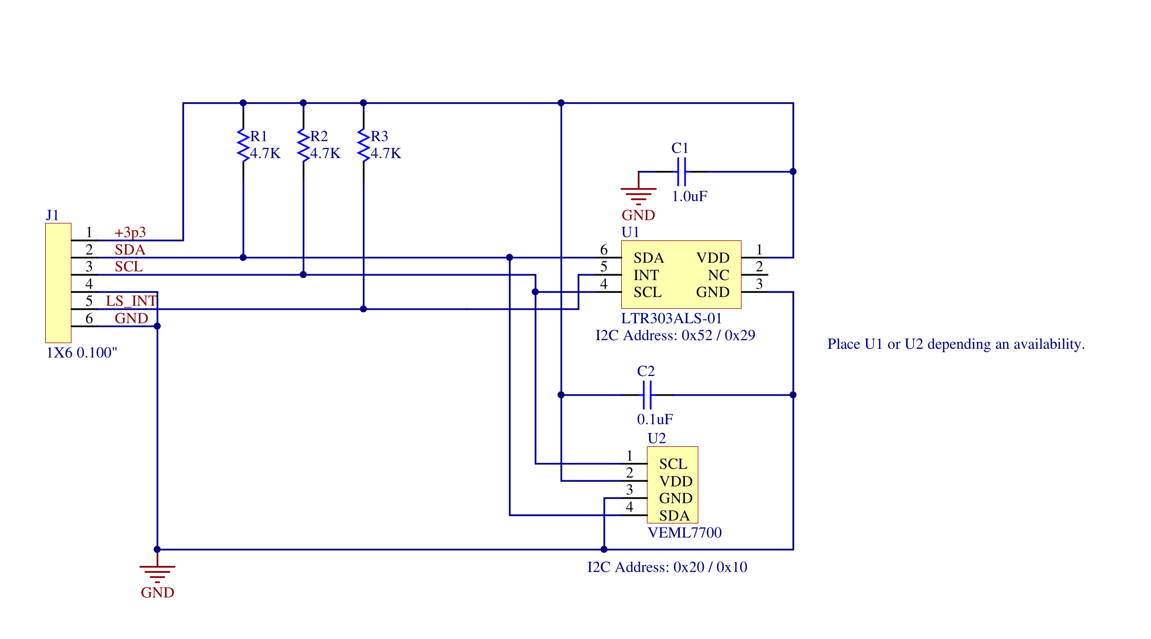
Ambient Light Sensor Board
03/14/2023 at 21:27 • 0 commentsIn a previous project that used more of the display modules, I used a multiplexer board to separate 12 matrix character displays into 3 different segments of one I2C bus. That multiplexer board has a single ambient light sensor on the back side. The ambient light sensor that I used has been completely unavailable for the last 2 years, so I laid out a new board with two sites for different sensors from different vendors. Both sensors communicate with the host via I2C and have different addresses so they could both be populated on the same board if you wanted to. One sensor is enough for complete function though.
![]()
Reading the ambient light level makes it possible for the system software to automatically dim the displays so it does not light up a dark room, but still maintains a bright enough image in a well lit room to be readable.
This system is using the Vishay VEML7700 sensor which does not have an interrupt output. Strangely, the LTR303ALS-01 interrupt only indicates that the light level is out of a programmed range, rather than the conversion complete function I would prefer.
-
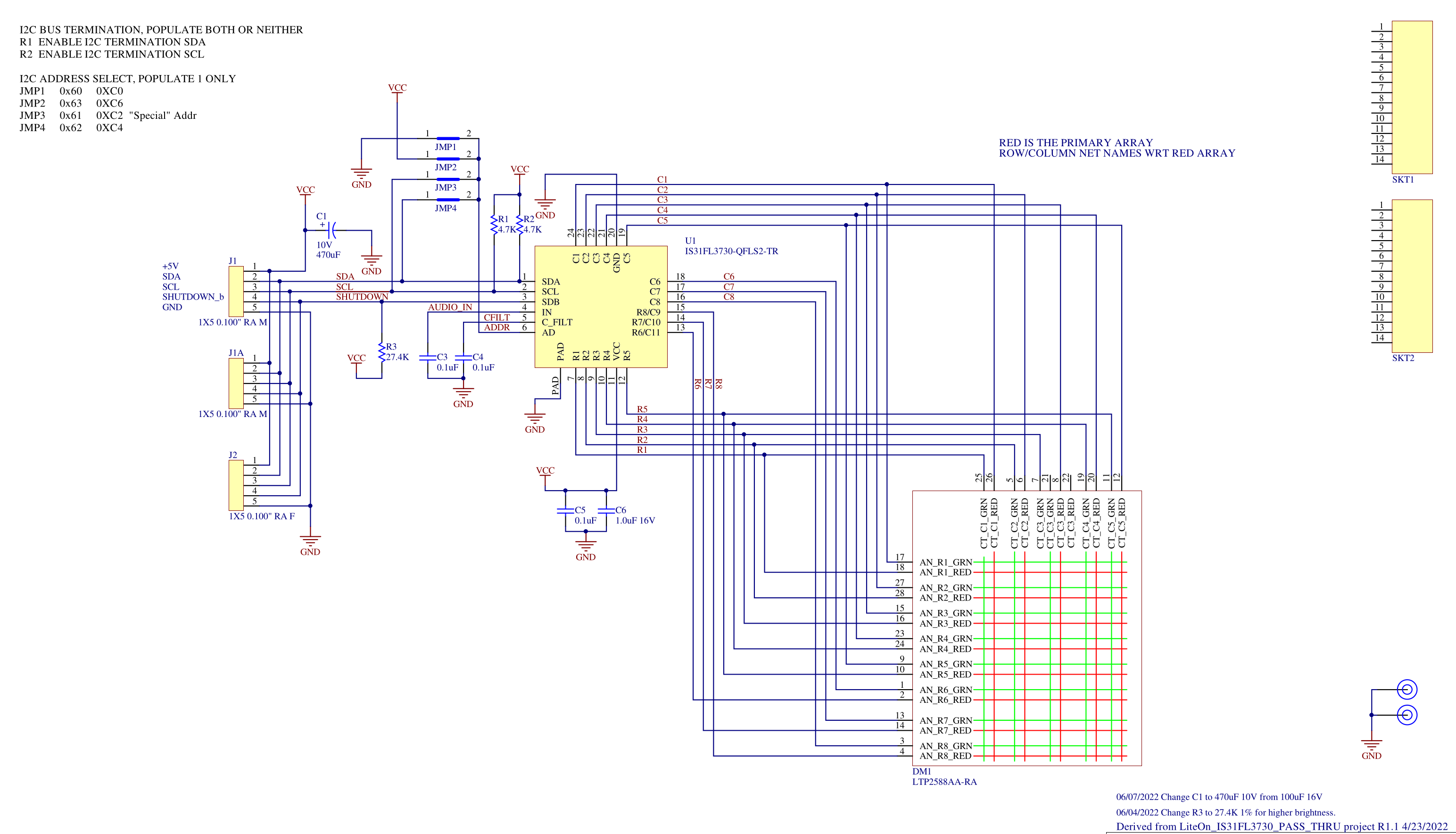
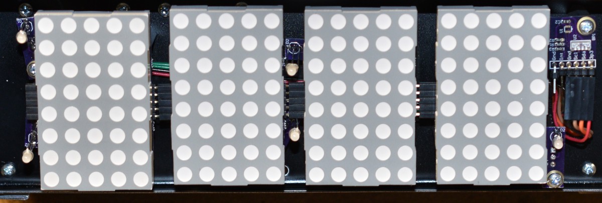
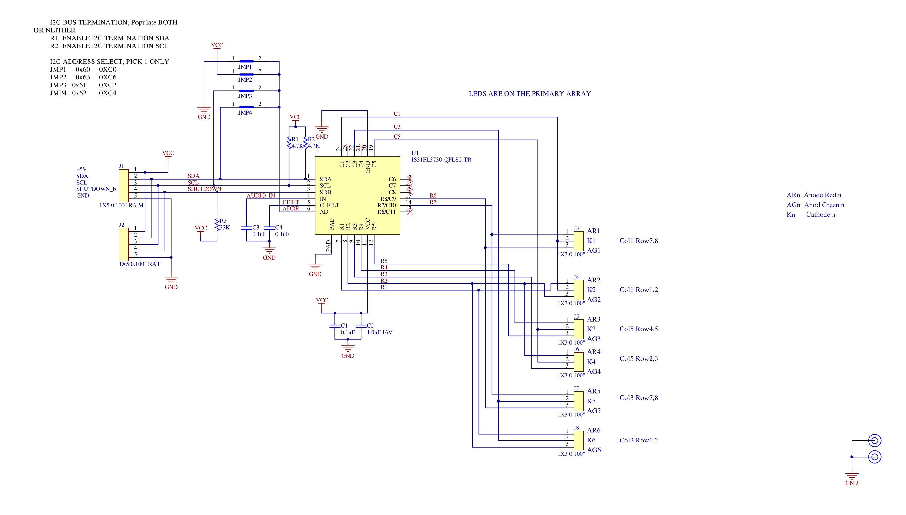
Matrix LED Display Driver Board
03/14/2023 at 21:12 • 0 commentsThis board design has been through numerous iterations, some for ease of use, some for cost reduction. Details can be found in my #LED Matrix Display project.
![]()
The IS31FL3730 chip drives the character matrix LED modules via I2C commands. Full control of all the connected LEDs including intensity is possible. Selecting a RED or Green character is also possible. The chips are pretty inexpensive at $1.20 each in quantities of 10. The LED matrix modules (LiteOn LTP2588AA) come from a local electronic surplus place. The LED matrix modules have Red and Green LEDs at each location.
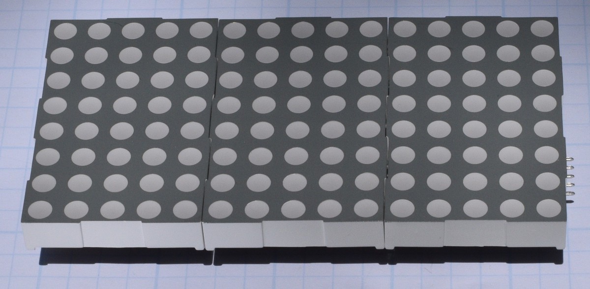
These boards can be stacked next to each other with up to 4 modules on the same I2C bus or segment. They can be assembled to have the LED modules in contact with each other for a continuous matrix of LEDs, or to have a physical gap between the LED modules. Here is an example of 3 boards built with the displays in contact with each other.
![]()
Having the physical gap between the LED modules allows you to get 1 character per module. The continuous matrix configuration lets you get 4/5ths of a character per matrix, so you would need 5 modules for 4 characters. This is because the characters are 5 columns wide by 8 columns tall, and you need at least one column of blank space between characters. The driver software becomes significantly more complex for the the continuous matrix configuration too. The plus side of the continuous matrix is that if you are scrolling characters across it, the continuous matrix looks a lot better. Using the physical gap between characters looks kind of jerky when scrolling. This point is moot in this project though since there is no scrolling. Things moving in my peripheral vision is extremely distracting to me, so scrolling displays were never considered for this project. Here is an example of 4 boards built with the physical gap between the displays.
![]()
Individual LEDs are controlled by the chip scanning rows and columns, so individual LEDs are switching on and off rapidly. This results in pretty sharp edges in the power supply current waveform. Originally, I had 2 10uF ceramic capacitors on each display module and it functioned, but looking at the waveform, I suspect it contributed to conducted emissions of EMI quite a bit. I replaced the two 10uF ceramic caps with one 470uF electrolytic cap, which helped slow the edges down, but I suspect the frequencies are too high for an electrolytic cap to fully solve.
-
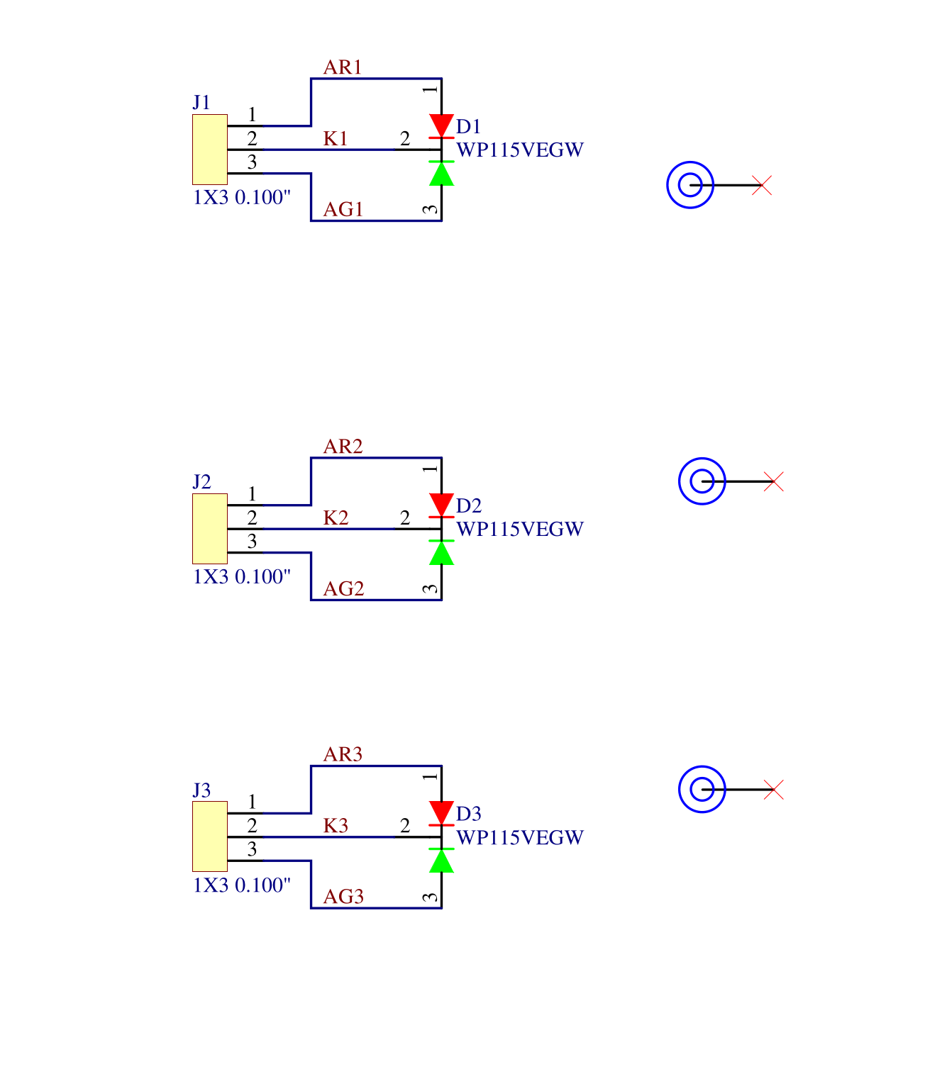
Miscellaneous LED Control Board
03/14/2023 at 20:33 • 0 commentsThis board is used to control the discrete LEDs that are on the front of the display. Those LEDs are combined Red and Green LEDs so they control much the same as the matrix LEDs for the character displays.
![]()
This board uses the same driver chip (IS31FL3730) that the character driver boards use, but only makes use of a few of the possible LEDs.
Two connectors with the same pinout as the character driver boards would allow this board to be plugged into one of the matrix LED driver boards, if the I2C addressing allowed. The I2C address is set via a jumper up in the upper left part of the schematic. In this project, there are not enough I2C address choices to put this board on the same I2C bus as the character driver boards, so it is not run as a pass through board. Software to control this board is derived from the software that controls the character driver boards.
The discrete LEDs are mounted on small boards with space for a mounting screw and a 1x3 2.54mm connector. In practice, I have just been soldering wires into these boards and putting the connectors on the end of the cables that plug into the Miscellaneous LED Control board.
![]()
There are 3 sets of LED, connector and bolt hole per "board". This is a crude panelization on my part. When I get the boards in, I cut them apart on the bandsaw. Most projects use a number of these boards, so getting them 3 at a time is good. This project uses 5 of these lndividual boards.
-
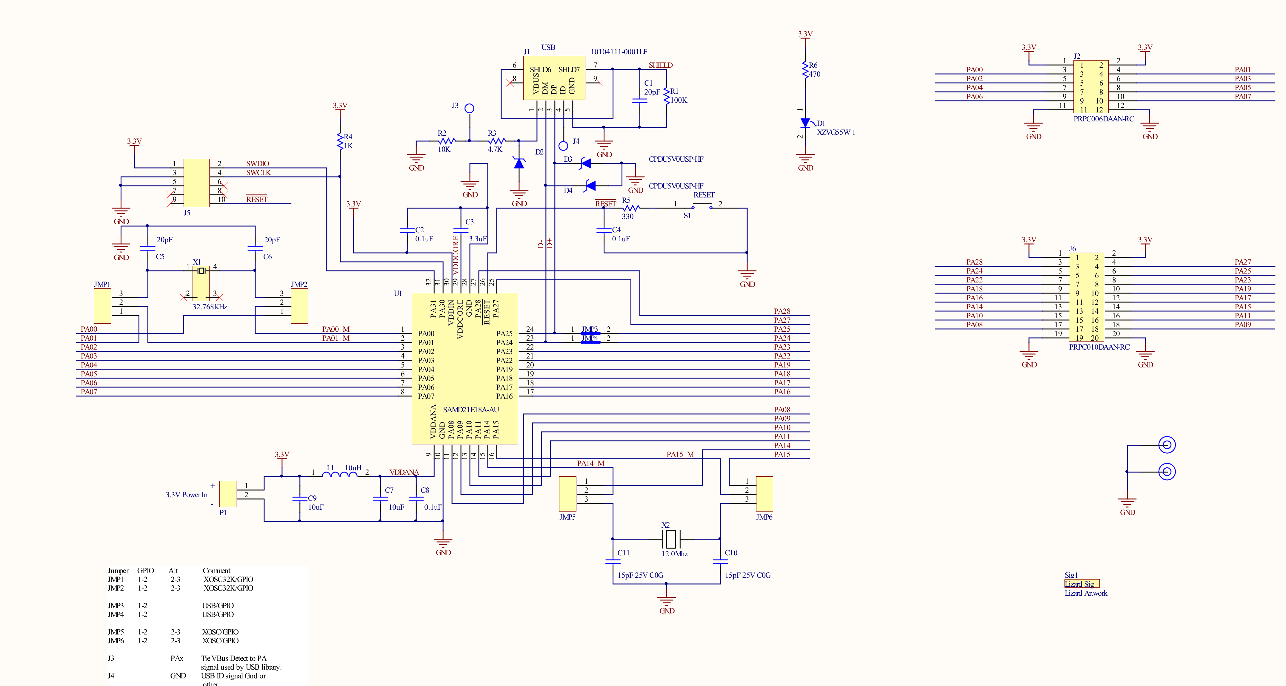
Processor Board
03/14/2023 at 20:11 • 0 commentsThis is a pretty minimal board.
![]()
It has the processor itself (ATSAMD21E18A), a 12MHz crystal, a 32.768KHz crystal, a JTAG connector and I/O signal connectors.
Since the crystal signals use GPIO pins, I put jumpers on to allow using the crystal or the two GPIO signals. Surprisingly, the 12MHz crystal is not useful, being too high to use as a reference for the PLL to multiply it up to 48MHz. This project is using the 32KHz crystal for the PLL reference and the GPIO signals that could go to the 12MHz crystal. The USB socket is not used at all in this project.
These chips are only starting to become available again after the chip shortage. Fortunately, I had an old test PCB left over from when I designed this board.
The board runs on 3.3V from the filter regulator board.
Serial I/O on the SAMD21 family is done with configurable blocks that they call Sercoms. Each one can be configured to operate as a UART, an I2C or a SPI port. The ATSAMD21E18A has 3 of these Sercoms. Two of them are in use as I2C ports, an one is configured as a UART for debugging.
Most of the GPIO signals on J6 are in use for one thing or another.
When I first started messing with this processor, I tried to write my own clock system configuration code. After bricking a processor chip by configuring the clock system in a non-functional way, I added a piece of code that tests two of the GPIO pins to see if they are jumpered together. If they are jumpered together, the code enters an endless loop. This test is run before entering the clock configuration code. In the event that I screw up the clock configuration again, I can put the jumper in and re-program the part. Without this code, it jumped into the clock config code before I could break to re-program it. People with more experience on this chip, may know a better way to deal with it. At this point, I have figured out the vendor supplied configuration stuff well enough that I have a working clock configuration for the projects that I use it on.
-
Clock Board
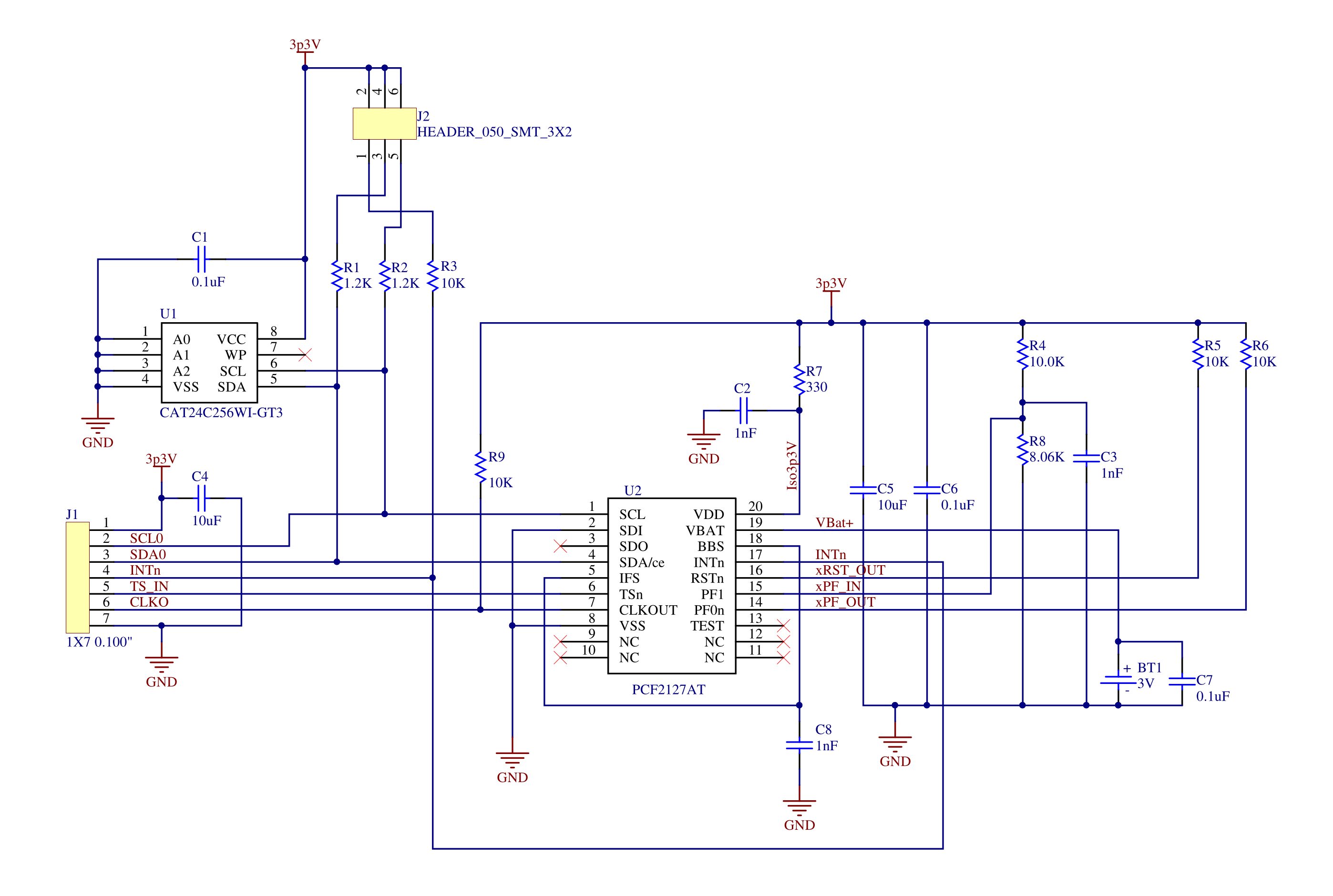
03/14/2023 at 17:28 • 0 commentsThis board has an NXP PCF2127AT clock/calendar chip on it. The schematic shows an EEPROM chip (CAT24C256WI on it, but it is not populated in this project.
![]()
The PCF2127 chip can communicate via an I2C bus or a SPI interface. This board uses the I2C interface. An interrupt signal (INTn) from the clock chip is used to signal the processor that the seconds value has changed, which means that you don't need to poll the chip over the I2C bus continuously. The interrupt signal is routed to a GPIO input on the processor where it is polled in the main loop. It is trivial to get the GPIO input data register, fetching the contents of an on-board hardware register compared to conducting a couple of I2C bus transactions. Reading the GPIO data register takes less than 100nS, while reading the clock register and resetting the internal address pointer takes about 200uS.
There is a small amount of RAM (512 bytes) in the chip which can be used to store non-volatile data. Clock operation and maintaining the RAM contents while the system power is off is done with a CR2023 battery. The switching between system power and battery power is done inside the chip.
The chip has provisions for accepting a signal for time stamping. This could be used to discipline the clock from a GPS receiver or something similar, but this system is not using that capability.
I have used this chip in several other projects, and the timekeeping is very accurate, good to a minute or less per year. -
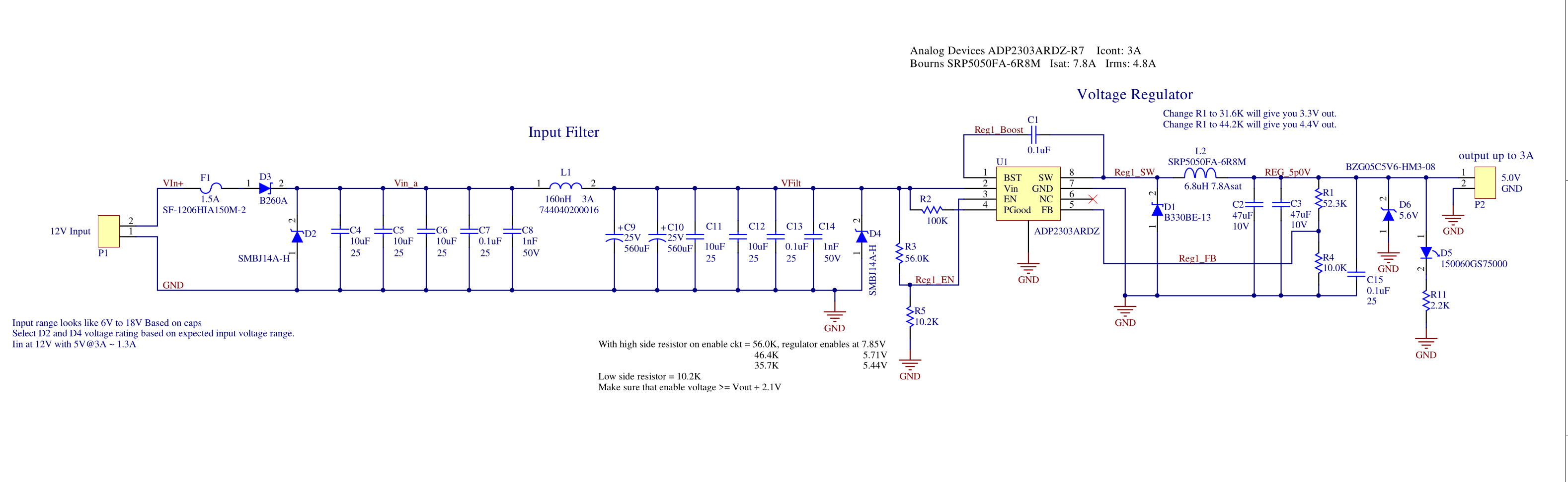
Filter Regulator Board
03/14/2023 at 16:59 • 0 commentsThis is the local power supply for the project. It will run on anything between about 8VDC and 14VDC in and outputs a regulated 3.3V out. The schematic is labelled as having 5V out, but the output voltage can be changed easily, by changing the value of the feedback divider resistor R1. In this project, R1 is 31.6K, which results in 3.3V out.
![]()
On the left side of the schematic is the input. A fuse protects the input source and to a lesser extent, the rest of the system. The voltage regulator is a buck type switching regulator. Buck regulators have a nasty failure mode where the switching transistor (inside the regulator chip in this design) shorts across. When the switching transistor shorts, it puts the full input voltage on the output of the regulator. Near the right side of the schematic is a zener diode D6 which will start to conduct if the output voltage rises about the specified voltage. If D6 conducts, it will clamp the output voltage to 5.6V, and if the switching transistor has failed, it will blow the input fuse. It is something of a race between the fuse blowing and the diode failing, hopefully the fuse blows first.
Back on the left side of the schematic, there are two diodes next to the fuse, D3 and D2. D3 is a schottky diode to protect the system from a reversed power supply input. D2 is a TVS (Transient Voltage Suppressor) diode which is pretty similar to a zener diode except it is optimized for suppressing fast spikes like ESD events. It will also protect the voltage regulator from over voltage inputs by blowing the input fuse.
After the diodes is a filter. Switching regulators can generate a lot of high frequency energy back into the input side, which in this system is likely to be a long wire to a wall wart power supply. This is called conducted emission. That long wire will radiate that energy, causing problems with any nearby TV or radio equipment. This is becomes radiated emission with the help of the input power cable. The purpose of this filter is to remove as much of that high frequency emission as possible.
In a previous iteration of this board, I had a more complex filter with a lot higher inductance. This made the regulator input look like an inductive load to the wall wart which caused serious startup and stability problems for the wall wart which is another type of switching regulator. The current design does a pretty good job reducing the conducted emissions, and does not irritate the wall wart.
Diode D4 (another TVS diode), after the filter is there to clamp any possible transients created by the inductance in the filter.
Finally, we get to the buck regulator itself. U1 is a variable output buck regulator with the switching transistor in the package. Previous iterations of this board had inductors (L2) that saturated at a current lower than the internal current limiting of the chip. If the inductor saturates, it stops looking like an inductor and destroys the regulator chip and sends the input voltage to the regulator output. The saturation current rating of the inductor used is above the internal current limit and this board design has been operating happily in several systems for a year or more.
Switching regulators are sensitive to the board layout and keeping the regulator chip U1, D1, L2, C2 and C3 very close together is important. The data sheet describes this in detail.
Resistors R1 and R4 make up the feedback voltage divider. The regulated output voltage is divided down to feed back into the error amplifier in the regulator chip.
Diode D6 has already been discussed in the section on the input fuse.
D5 and R11 are just a pilot light to show that there is voltage out of the supply.
The output connector shown has a single + and - output terminal. A later revision of this board has 4 outputs for each. This will simplify the wiring harness construction by avoiding in-line splices on the power distribution.
It is not shown on the schematic here, but the ground (GND) connection goes to the mounting screw pads to connect to the metal chassis ground.
Simple LED Matrix Alarm Clock
A Fairly Conventional Alarm Clock using LED Matrix Displays