In this previous log I described the new bankswitching system. But I wanted to add another mode (Linear mode). It would be nice if a program could access the whole 512kB memory without bankswitching. The address would be in a 3-byte register, with 19 significant address bits. A simple processor with 19-bit addresses could then be implemented.
For programming the Z80 or 6502, it is not needed to know all this. You only need this if you implement a bankswitching system or a new processor microcode that accesses the whole memory. Probably it is only for myself.
I came up with the following: (All images can be enlarged by clicking them)

LINEAR MODE
The functions are essentially the same as in the mentioned previous log, but I added the Linear mode. For program code, the upper bits A18 and A17 come from a bank select register, and A16 comes from microcode. For data, upper bits A18, A17 and A16 come from another bank select register. So, the upper three address bits can be different for program and data. Also new is, that this bank select register can be loaded from a memory-resident register in a single cycle.
APPLICATION and KERNEL
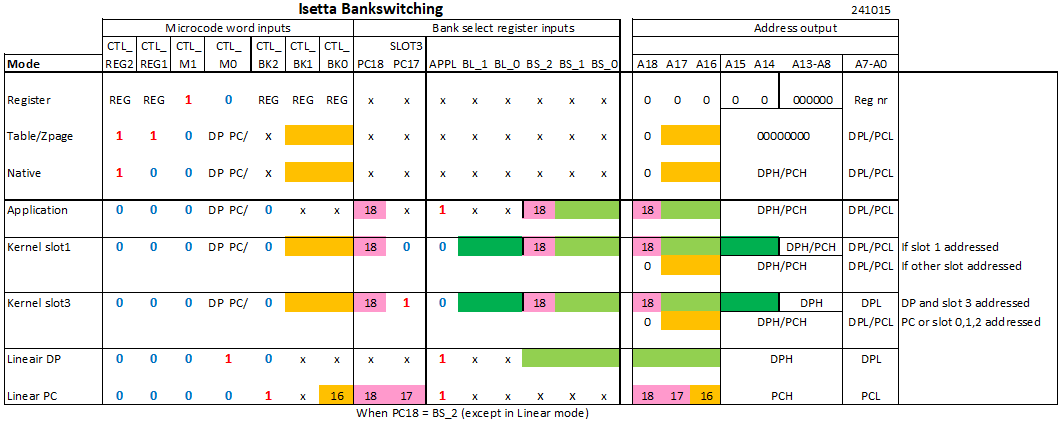
It is intended that, for Application and Kernel modes, BS_2 and PC18 are always written with the same value. That makes our table slightly less complex:

This diagram shows all modes. The modes are controlled by signals in the microcode and the bank select registers, as shown.
HARDWARE IMPLEMENTATION
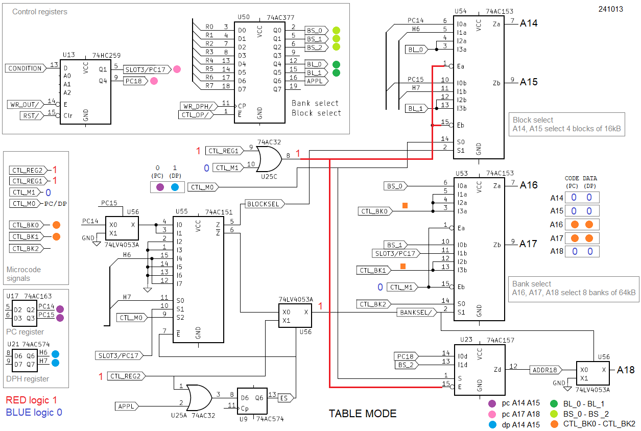
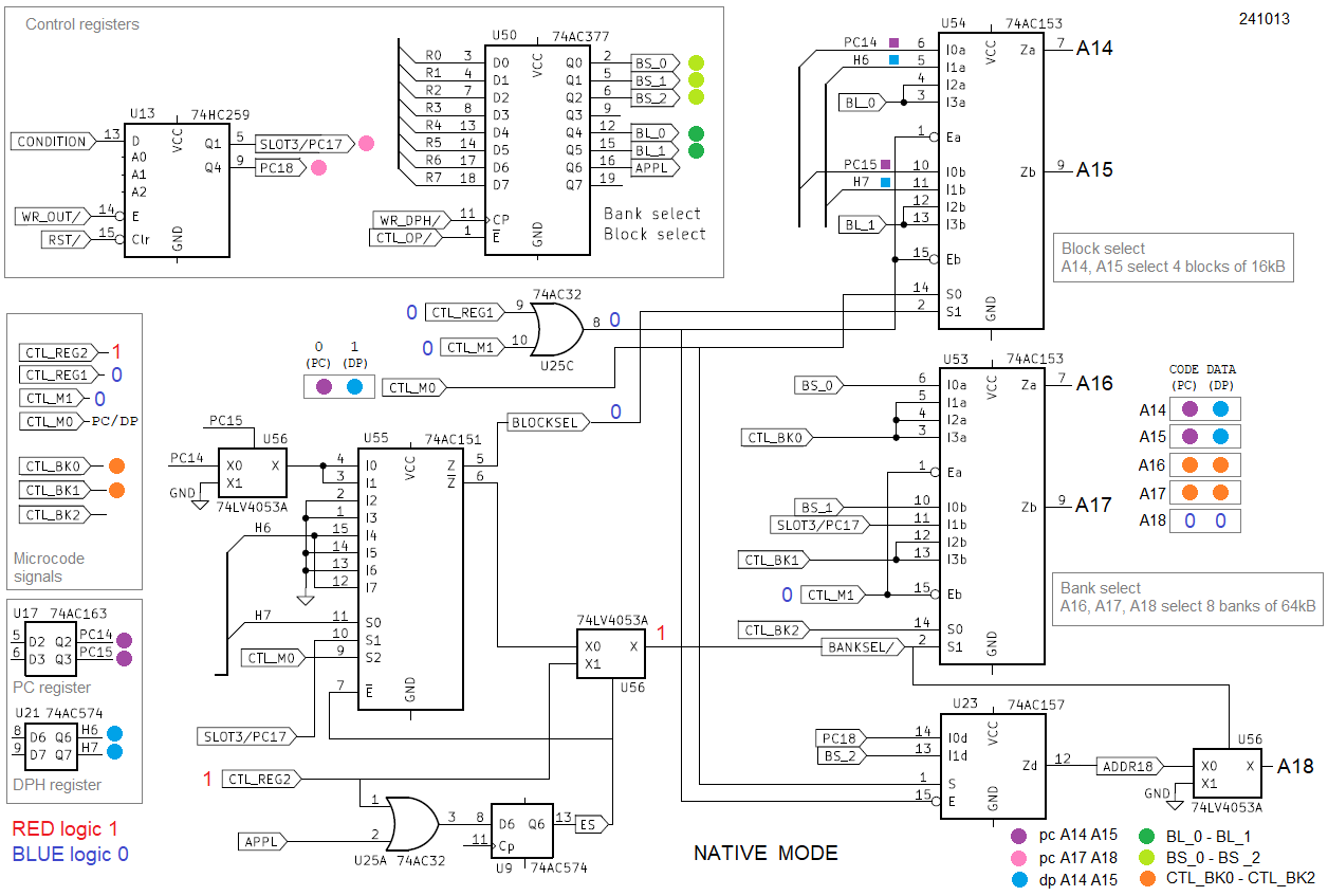
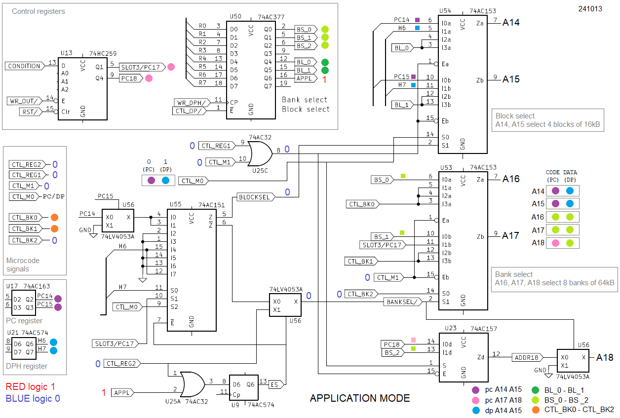
The result is a bit complex because I didn't want to add more chips. Another complication is, that the address must be available quite fast, so there can not be long propagation delays. The following diagrams (there are seven) explain all modes, and also the way it is implemented. The used colors are the same as in the table above.
You find the bankswitching control registers at the top of the diagram. The microcode control signals are at the left side. At the right side, you find the five highest address bits, their value indicated by '0' or a color.
REGISTER MODE

This is the simplest. The (memory resident) registers are in the very first 256 bytes of memory. This mode is selected by CTL_M1 = 1. The CTL_M1 signal switches all upper address outputs OFF, so all upper address bits are zero. The register in question is selected by several bits in the microcode.
The value in the bank select registers is irrelevant.
TABLE / ZPAGE

In this mode only the lower 8 bits of a data or code address are used. The other bits are zero, but A16 and A17 come from microcode. It is used for 6502 Z-page, for an identity table and a shift-right table. If A16=0 and A17=0, this mode can not be used (that is the domain of the memory-resident registers).
This mode is selected by microcode signals only. The value in the bank select registers is irrelevant.
NATIVE

This is the main addressing mode of the first prototype. The upper address bits are 'hardwired' in the microcode. Bit A18 can no longer be used, that should not be a big problem because this will no longer be the main addressing mode.
This mode is selected by microcode signals only. The value in the bank select registers is irrelevant.
APPLICATION MODE

Here, the upper three address bits are freely programmable in the bank select register U50. It is advisable to set BS_2 equal to PC18, otherwise the topmost address bit is different for code and data (also for the following two modes kernel slot1/slot3).
This mode is selected by microcode signals in combination with APPL = 1. Yes, the APPL signal got it's name from this mode.
KERNEL SLOT1

The 64k addressing range is split up in four slots:
- Slot 0 ( 0000 - 3FFF )
- Slot 1 (4000 - 7FFF)
- Slot 2 (8000 - BFFF)
- Slot 3 (C000 - FFFF)
In this kernel-slot1 mode, normally the microcode selects which 64k bank is selected (orange signals). But if the address is in slot 1, the bank number comes from the bank select register (light green). The 16k block within that bank is also selected with that register (dark green).
This mode is selected by microcode signals in combination with APPL = 0 and SLOT3 = 0.
The 74AC151 is enabled because APPL is low. It looks at the value of the A15/A14 bits of the relevant register (DPH or PCH). If this bits indicate the range of Slot 1 (4000 - 7FFF), the multiplexers at the output will change to the banknumber and block number that are stored in the bankswitch register.
KERNEL SLOT3

Here, if the address is in slot 3, the bank number comes from the bank select register. But for the program counter, the bank number is always in microcode.
This mode is selected by microcode signals in combination with APPL = 0 and SLOT3 = 1.
The 74AC151 is enabled because APPL is low. It looks at the value of the A15/A14 bits (only if the DPH register is selected). If this bits indicate the range of Slot 3 (C000 - FFFF), the multiplexers at the output will change to the banknumber and block number that are stored in the bankswitch register. If the PC is in the range of slot 3, this will not be detected.
LINEAR MODE

For program code, the upper bits A18 and A17 (pink) come from the bank select register, and A16 (orange) comes from microcode. For data, upper bits A18, A17 and A16 come from another bank select register. So, the upper three address bits can be different for program and data.
For addressing data, this mode is identical to the APPLICATION mode.
But for addressing code (with the PC), the microcode must set CTL_BK2. That will cause different A16 and A17 bits to be selected by U53. Of course, it is not required that BS_2 is equal to PC18 in this mode.
Discussions
Become a Hackaday.io Member
Create an account to leave a comment. Already have an account? Log In.