 gedm-dev
The heart of the G-EDM will get a new design. After merging the 12v PSU into the spark generator it started to produce same heavy voltage drops on the feedback signal sometimes. So the grounding had some issues on the PCB.
The new PCB will have a gnd plane concept with power and logic gnd merged at one point.. Also the mosfet will be switched in a high side configuration. Low side switching may produce oscillation and stuff that is not wanted after the noisy spark flushes to gnd through the mosfet.
Had a hard time figuring out how to create a high speed, high current, high side N-Channel Mosfet switch. Bumpy ride from bootstrapping to charge pumps and level shifters.
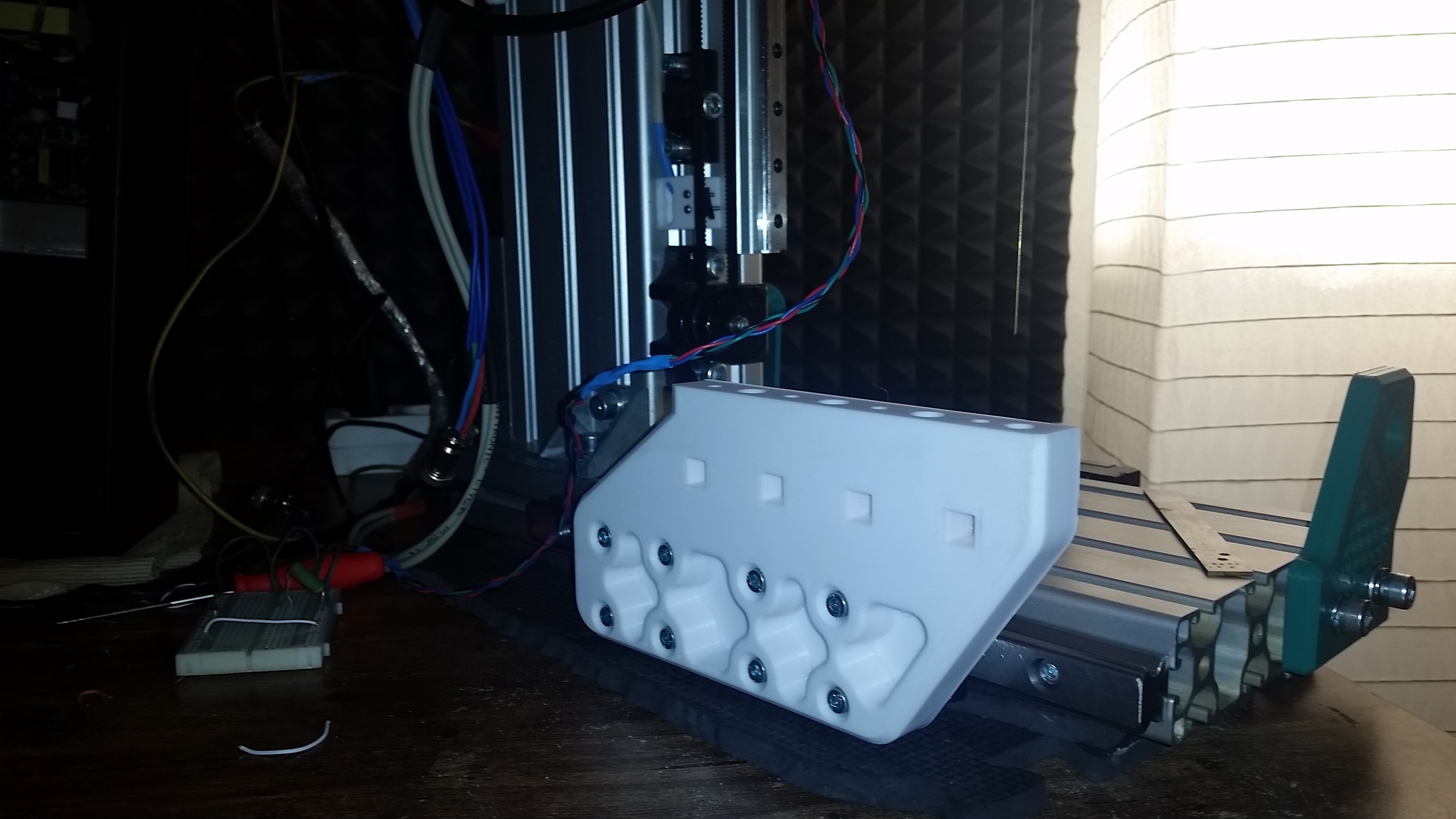
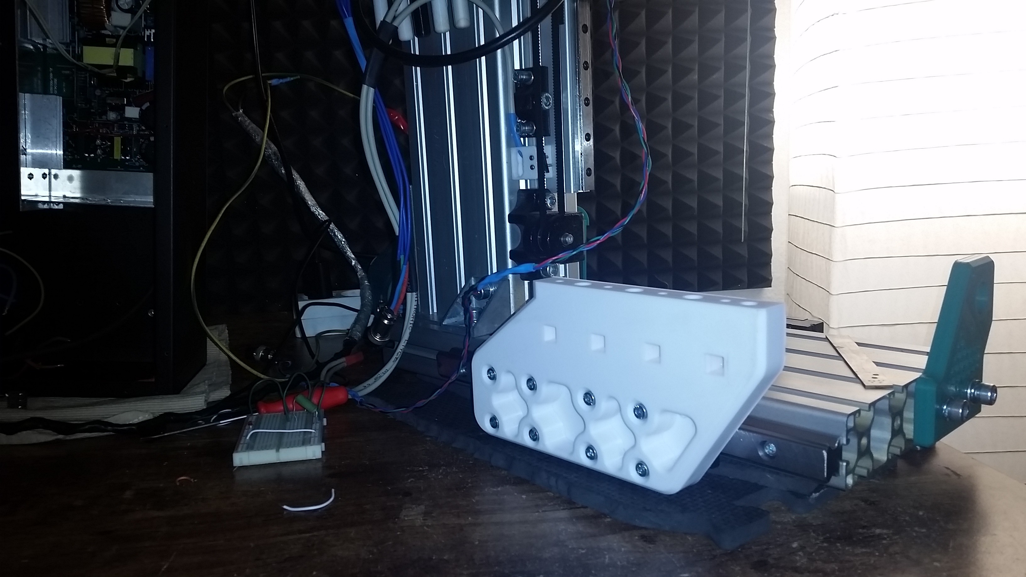
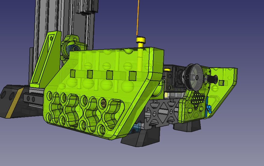
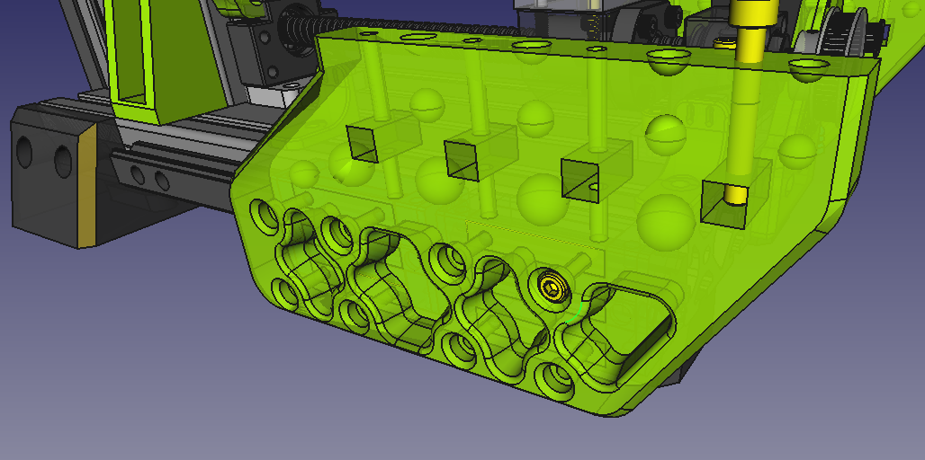
X axis is still printing but the first sidewall is ready. 20mm thick PLA+. Those things are massive.
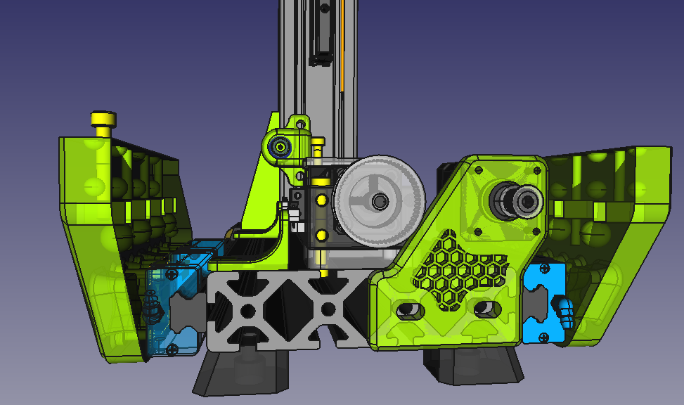
The CAD object:
Discussions
Become a Hackaday.io Member
Create an account to leave a comment. Already have an account? Log In.