 Dr. Cockroach
I have been working on a replacement for the PC register that I had before. I was not pleased with how well it worked and decided to switch to pnp transistors. The following photos show what I came up with and the steps in writing and storing data. In this case the number 2.
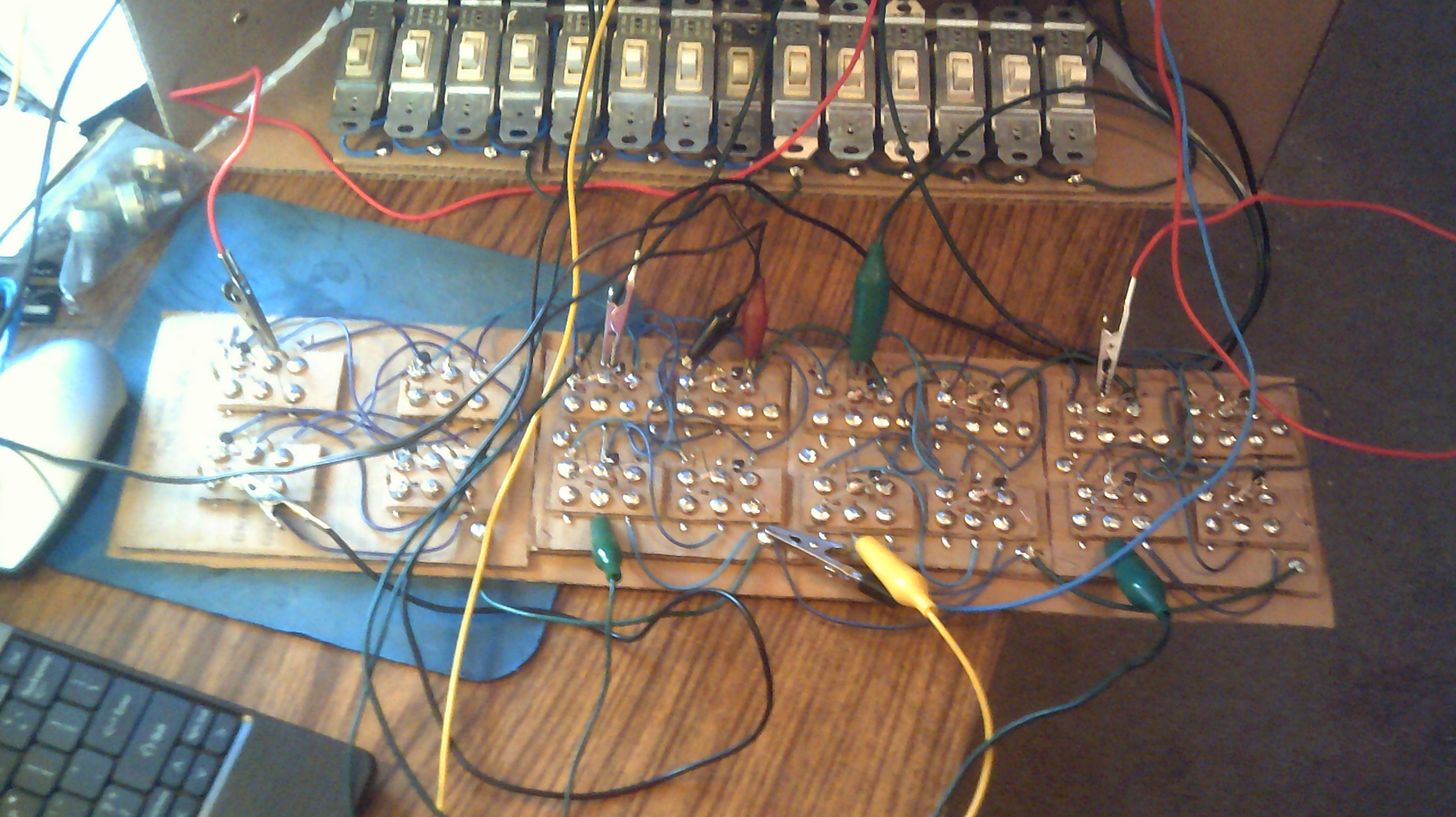
This is the register input and output zeroed.
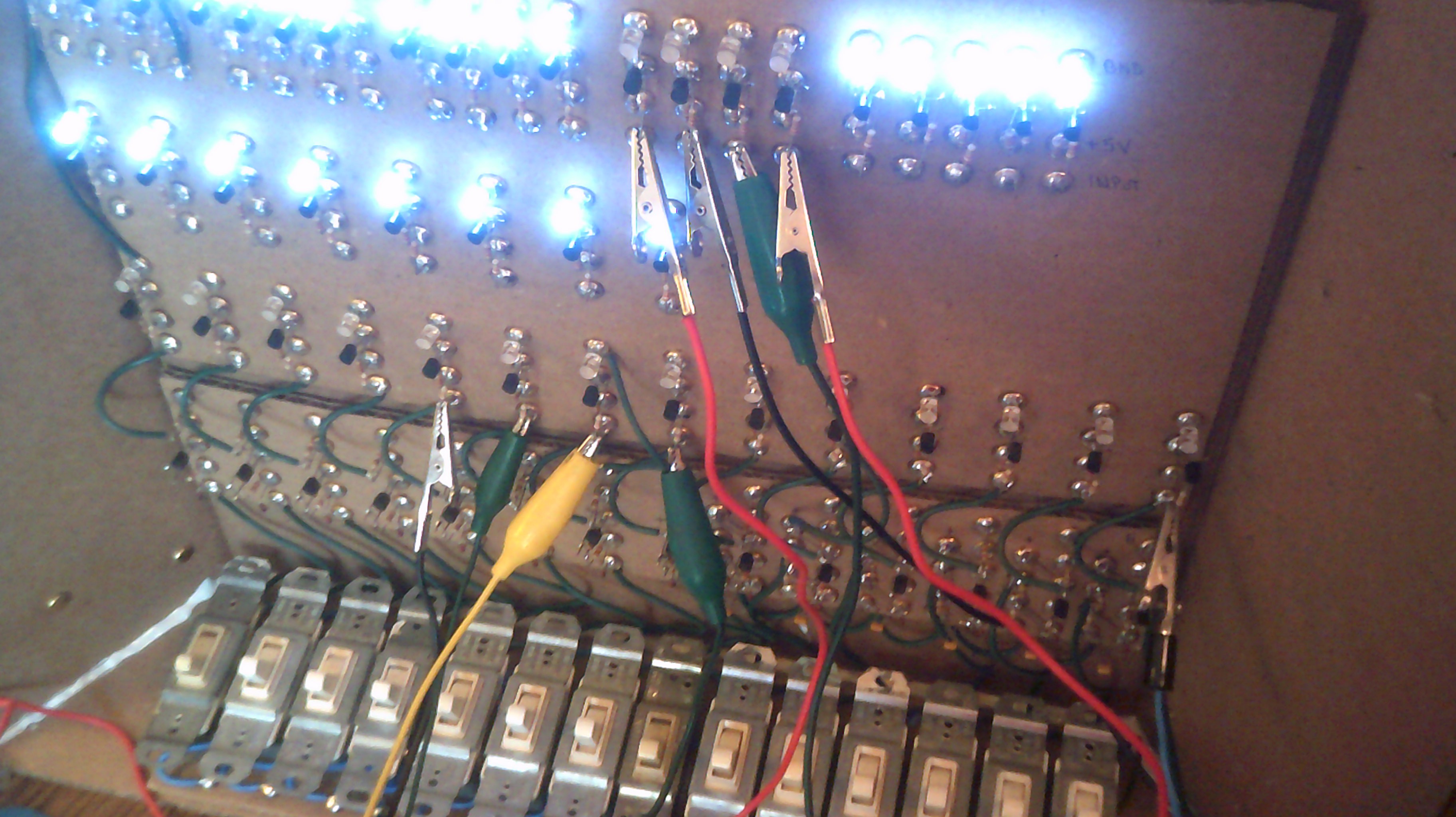
This is the number 2 selected on the input.
This is 2 on input with deposit selected ( far right switch )

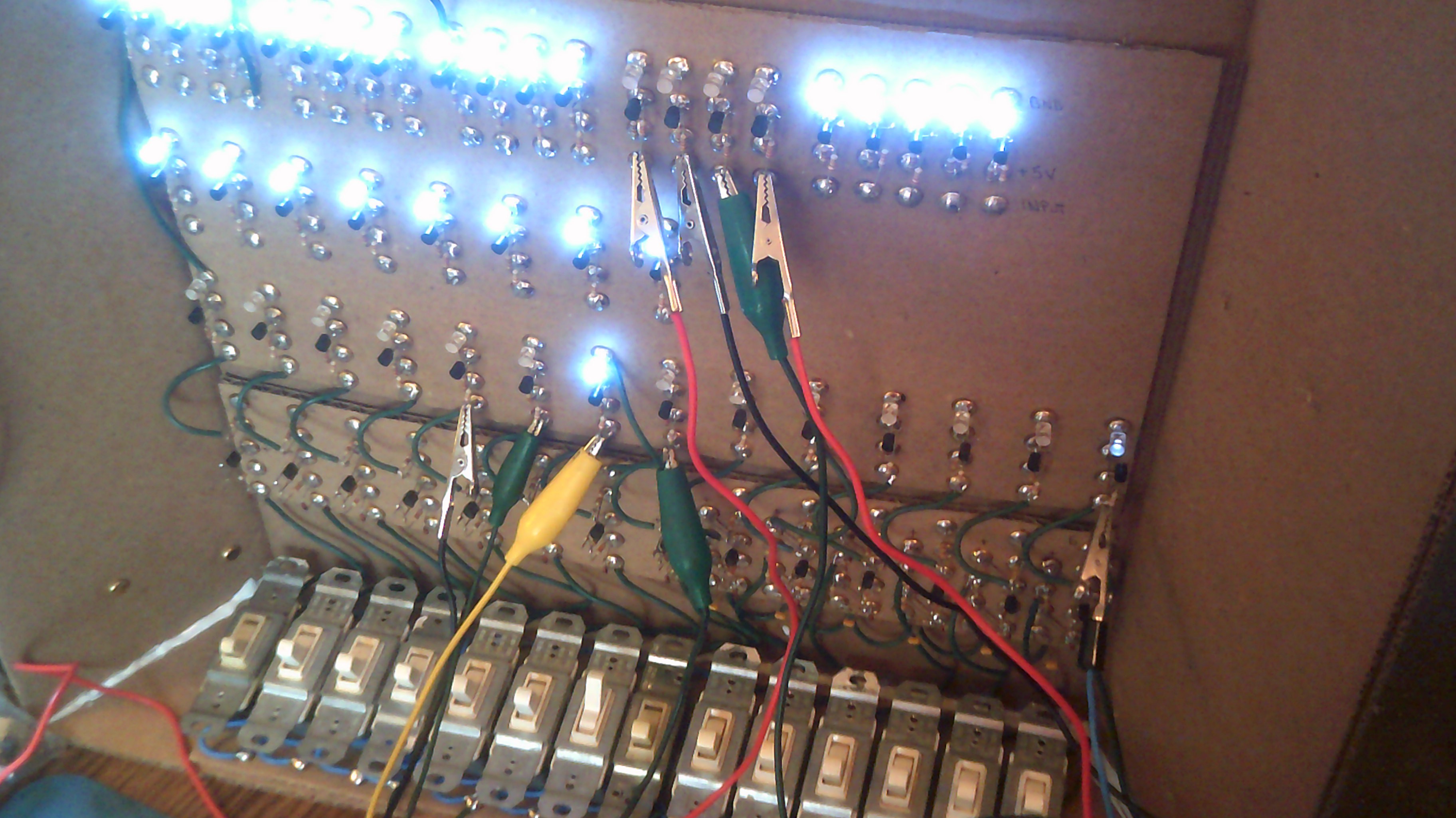
This is 2 latched on the output.
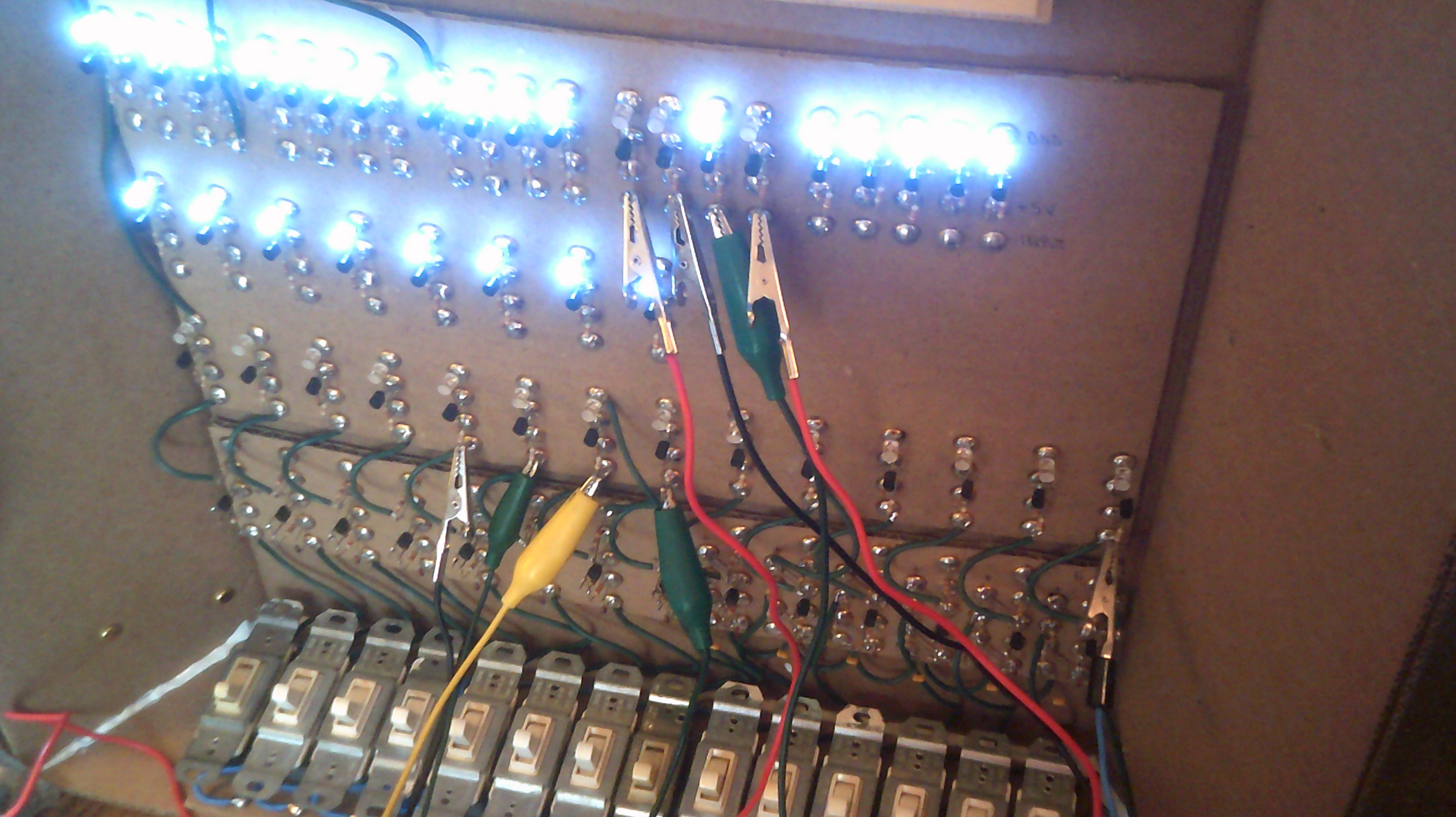
All four bits are latching and all is well except that when any of the input switches are set to one, then there is a little back voltage to the deposit led. This does not affect the memory from working and at least it lets me know that there is something to deposit ;-)
Discussions
Become a Hackaday.io Member
Create an account to leave a comment. Already have an account? Log In.
How many nibble registers do you need for the whole design?
Are you sure? yes | no
Hi Ted, I am looking at four for this build. Accumulator, B, W and PC. Accumulator and B will pretty much be tied to the ALU, the W will be a general use working register and the Program Counter. You could say I wired up a memory stick :-D
Are you sure? yes | no