Dr. Cockroach
-
February 8, 2017 - 1 nibble memory with pnp nand gates
02/08/2017 at 18:48 • 2 commentsI have been working on a replacement for the PC register that I had before. I was not pleased with how well it worked and decided to switch to pnp transistors. The following photos show what I came up with and the steps in writing and storing data. In this case the number 2.
![]()
This is the register input and output zeroed.
![]()
This is the number 2 selected on the input.
![]()
This is 2 on input with deposit selected ( far right switch )
![]()
This is 2 latched on the output.
![]()
All four bits are latching and all is well except that when any of the input switches are set to one, then there is a little back voltage to the deposit led. This does not affect the memory from working and at least it lets me know that there is something to deposit ;-)
-
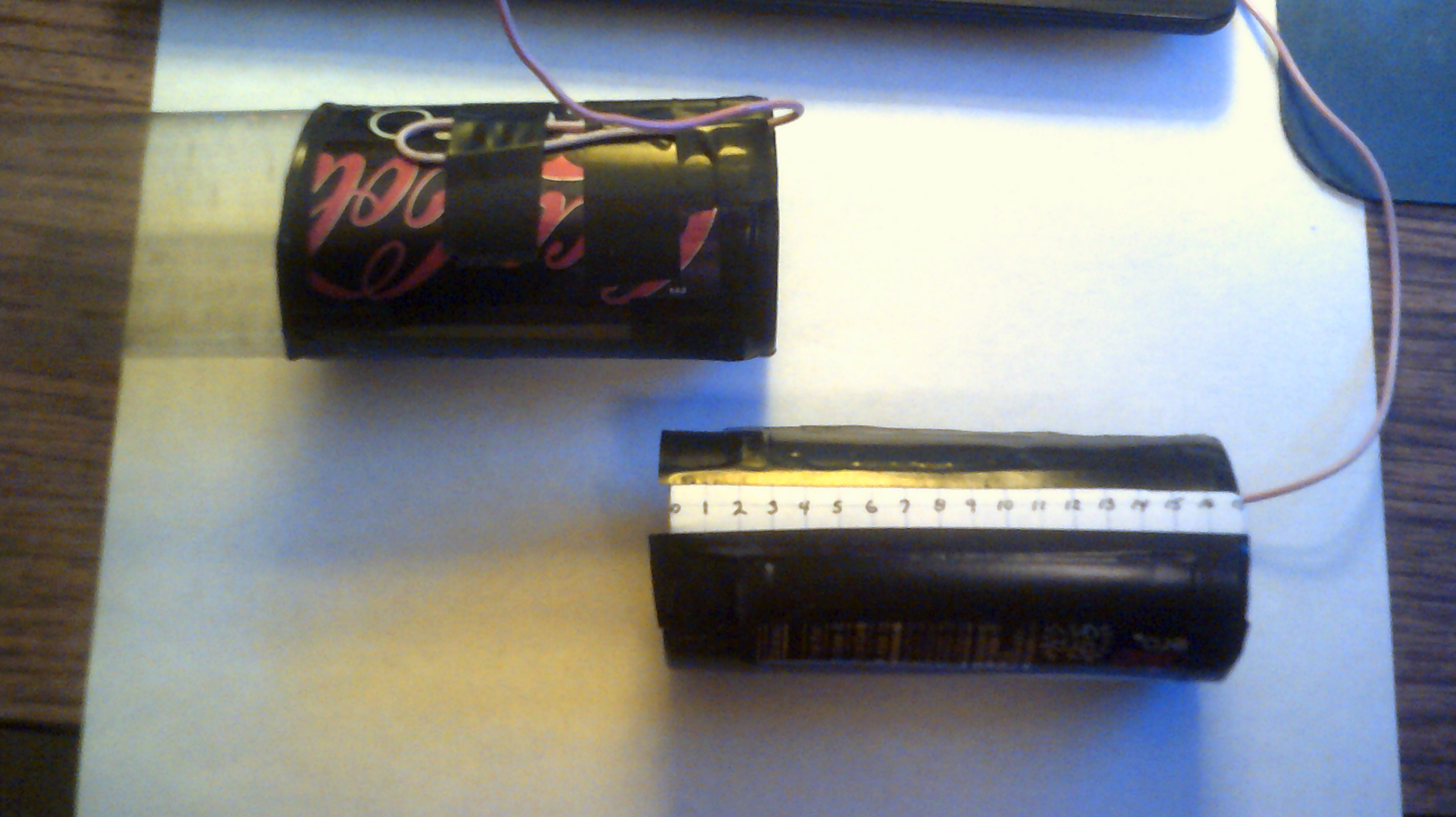
February 5, 2017 - And now for something different
02/06/2017 at 00:12 • 5 commentsJust dug out something from my junk box of parts that I almost forgot about.
I used to be very active with crystal radios and one day I wanted to see if I could make my own variable capacitor. Using two soda cans, a cardboard ( what else ) loo tube , electrical tape and a plastic tube, I was able to come up with this. Wired up with a crystal radio set it tunes quite nicely on the mw broadcast band here in the U.S.
Hope this gives everyone a smile :-)
![]()
![]()
-
February 4, 2017 - Sequencer installed
02/04/2017 at 11:41 • 2 commentsI have taken some time off of the actual build to study this project but now starting to melt some solder again. The sequencer has now been mounted to the main frame and is working very well. I was having a problem with the J-K flip-flop toggling without error. It would hang up from time to time and freeze for a couple of clock cycles and then resume again. Just by chance, I installed a led to the output of the pulser circuit and not expecting to see anything due to the short duration of the pulse. I do get a nice flash from the led and now the J-K is toggling without any glitches :-) I can only surmise that the led is placing a slight load on the pulser circuit but beyond that I am open to thoughts about why it works better.
Here is the result so far. The pulser is at the top right with the pulsed led on the right side of the board. The toggled J-K is in the middle and the sequencer is at the bottom with five steps that I can branch from. Sorry for quality but cheap camera ;-)
-
January 21, 2017 - Trouble in paradise
01/21/2017 at 16:02 • 7 commentsEver have one of those days where nothing goes right? I have been rewiring my program counter and using a circuit that is known good by a number of sources and yet no matter what I do, I can not get it to do anything. Just sits there mocking me. Oh well, that's the price I pay for taking on this project. Never fear, I will figure it out. Transistors and diodes test good. Wiring checks out and solder joints making good contact. I will survive , I will win :-)
-
January 17, 2017 - Power/ground bus wiring
01/17/2017 at 14:48 • 9 commentsTaking a day to wire up a master power switch and power / ground bus module. With this I will route power and ground connections to each panel. The module is nothing more than the switch and more brass fasteners at the top of the I/O panel.
-
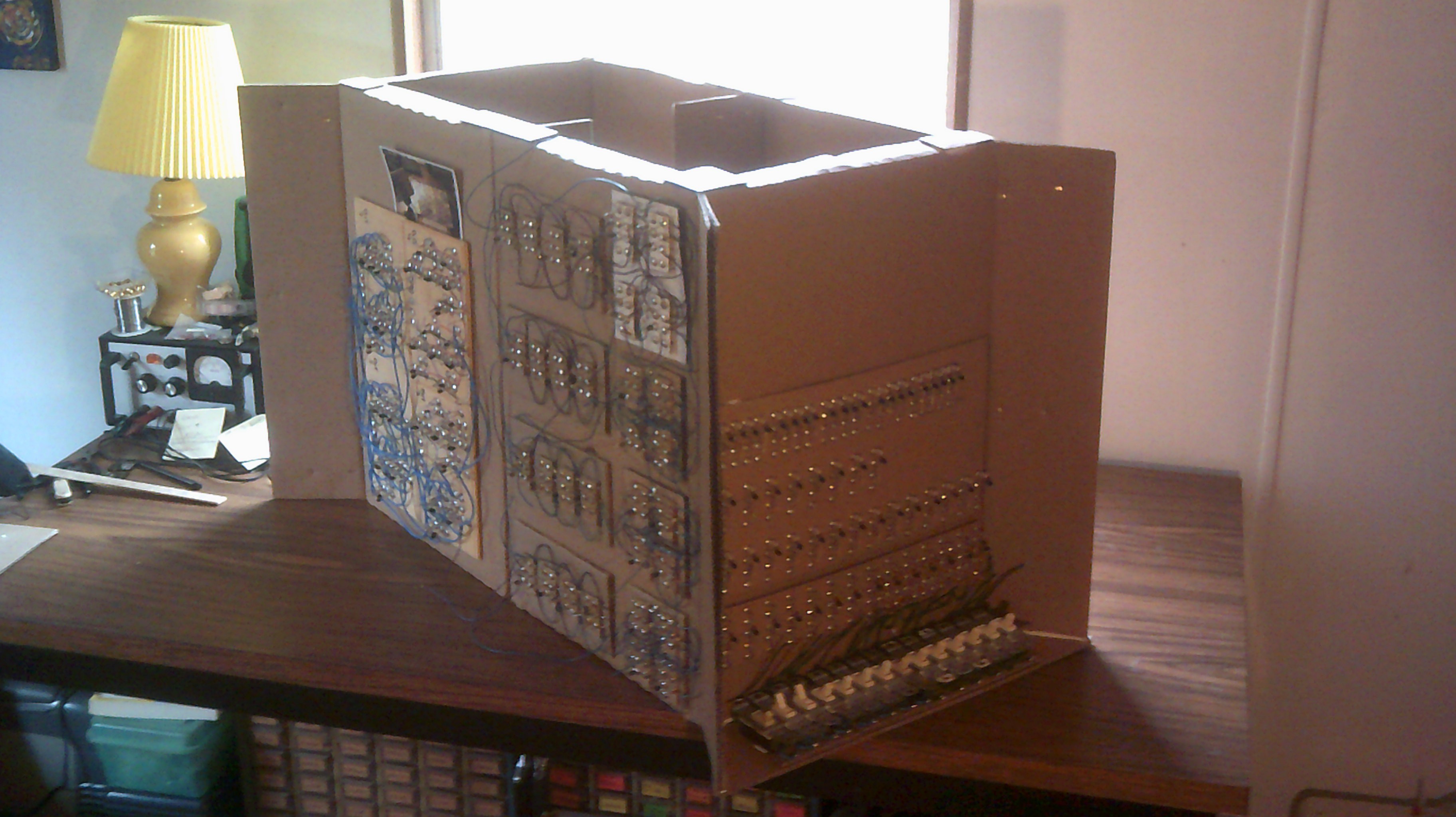
Over all view of current construction
01/15/2017 at 00:20 • 8 commentsThis is currently where I am at with this build. Does not look like much but when wiring the way I am then time drags on :-)
Same confusing circuits but now with a new look. At least it will now fit through the room door when it is time to move :-)
![]()
![]()
-
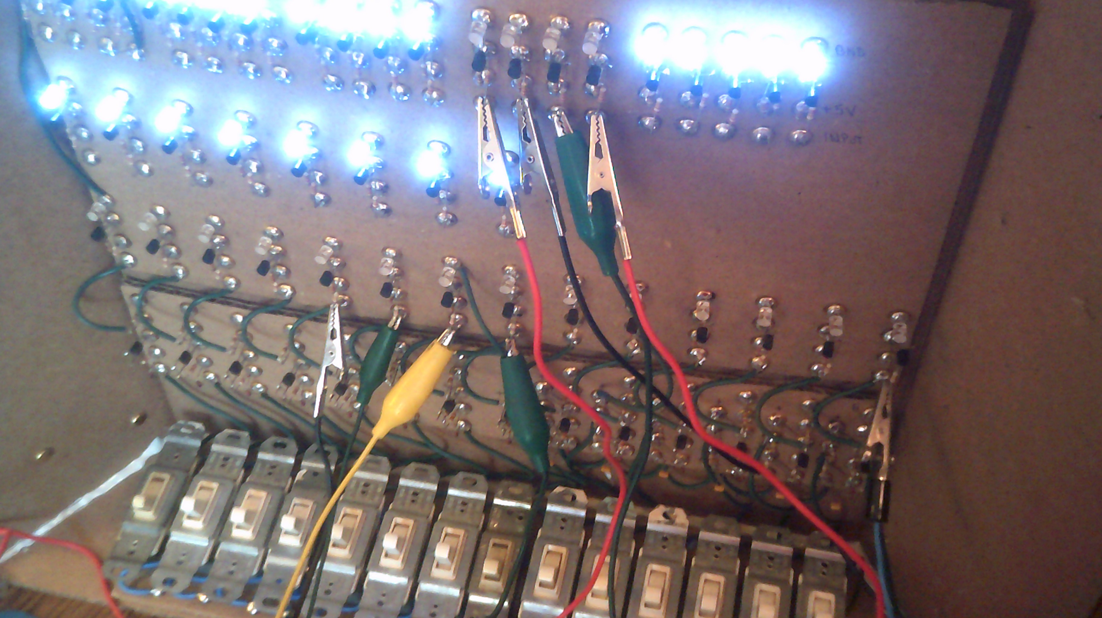
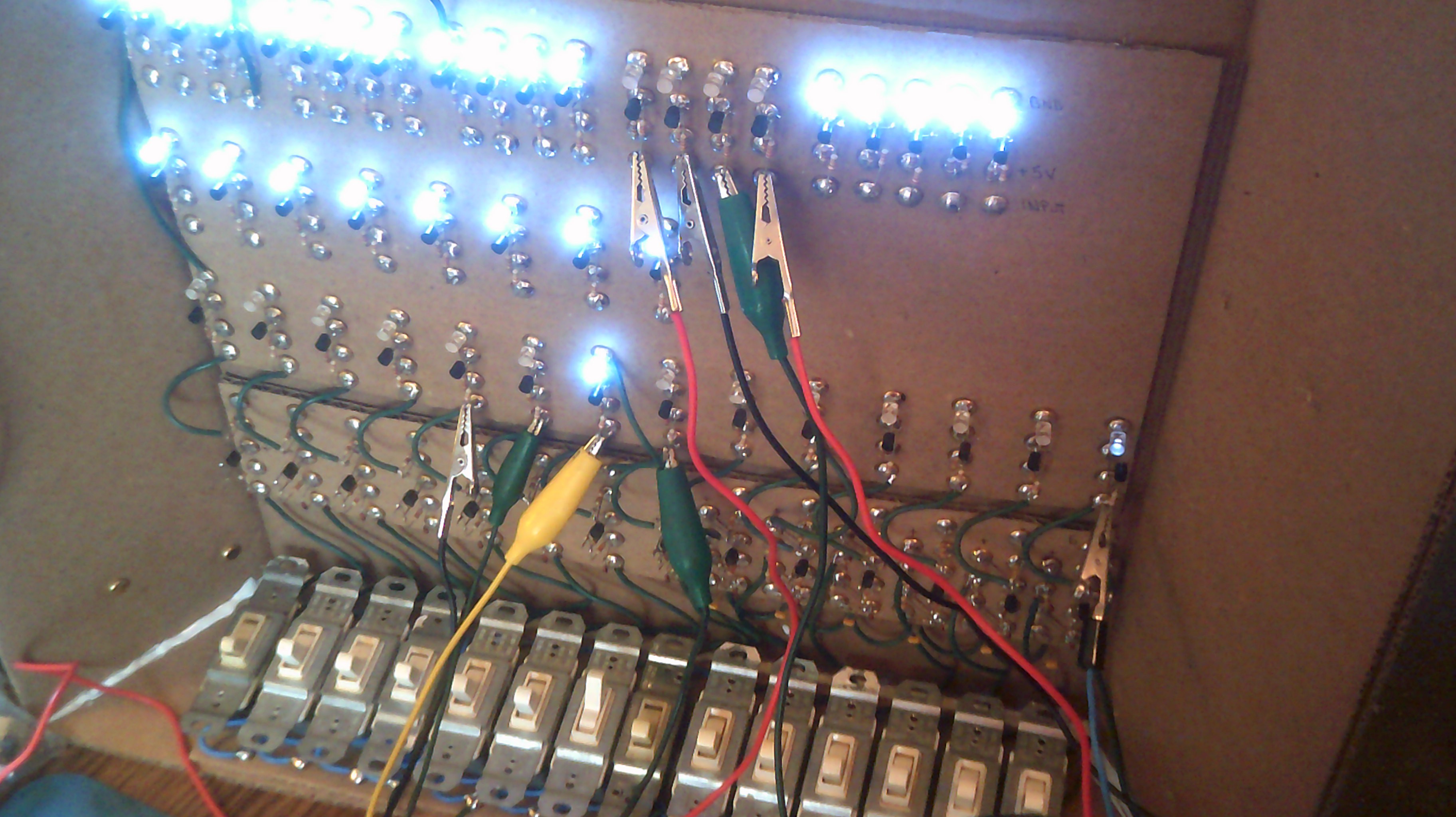
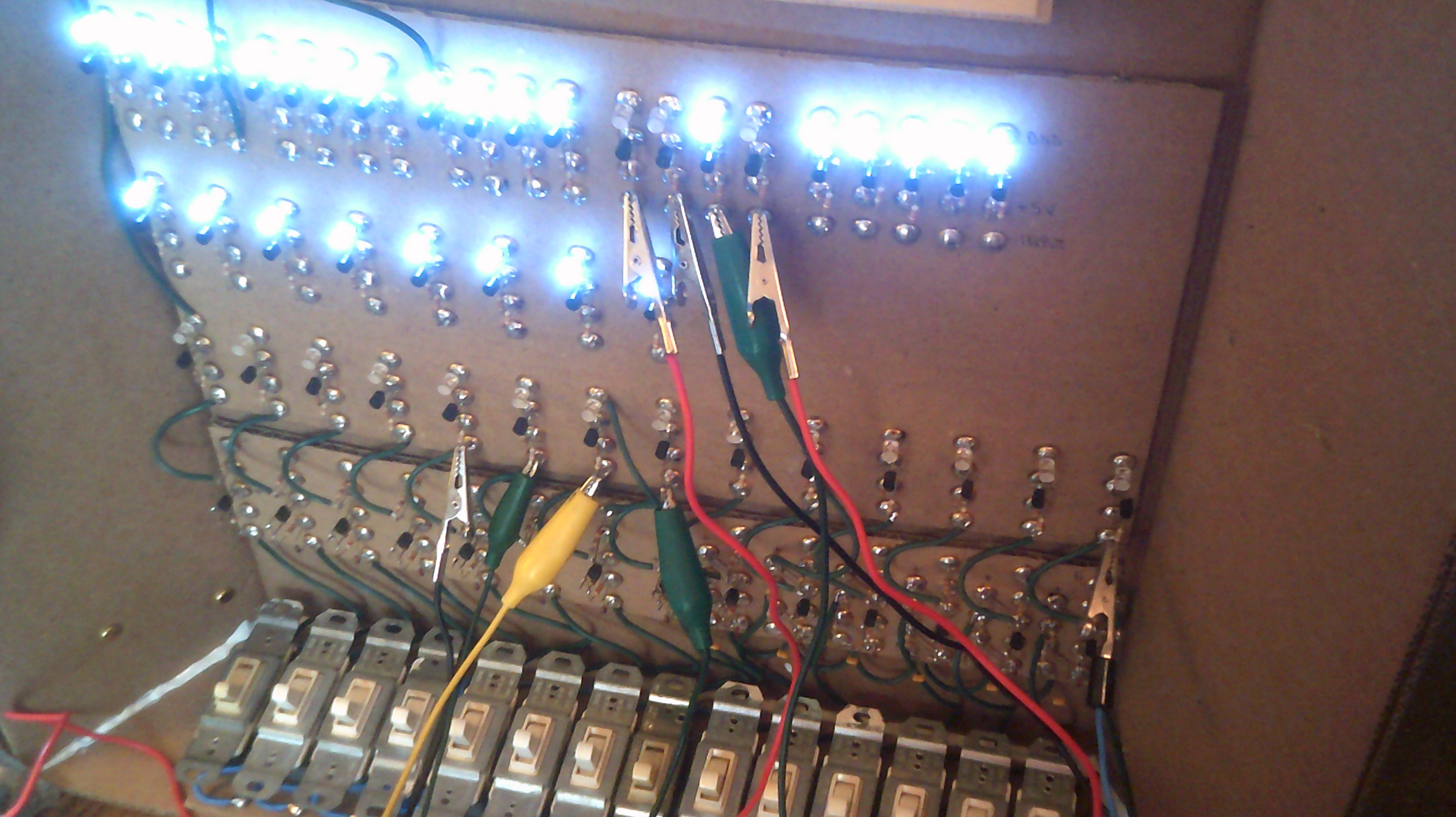
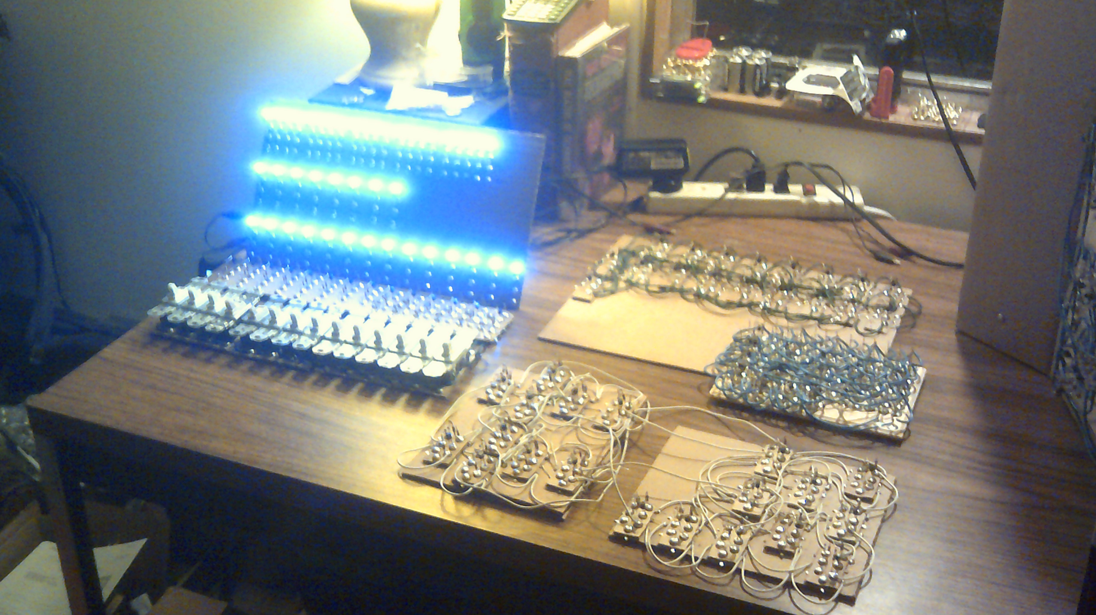
Input / Output main panel
01/15/2017 at 00:11 • 0 commentsThis the combined work so far on both the switch, interface and display panels. All that is left is to mount and interconnect the three sections
![]()
-
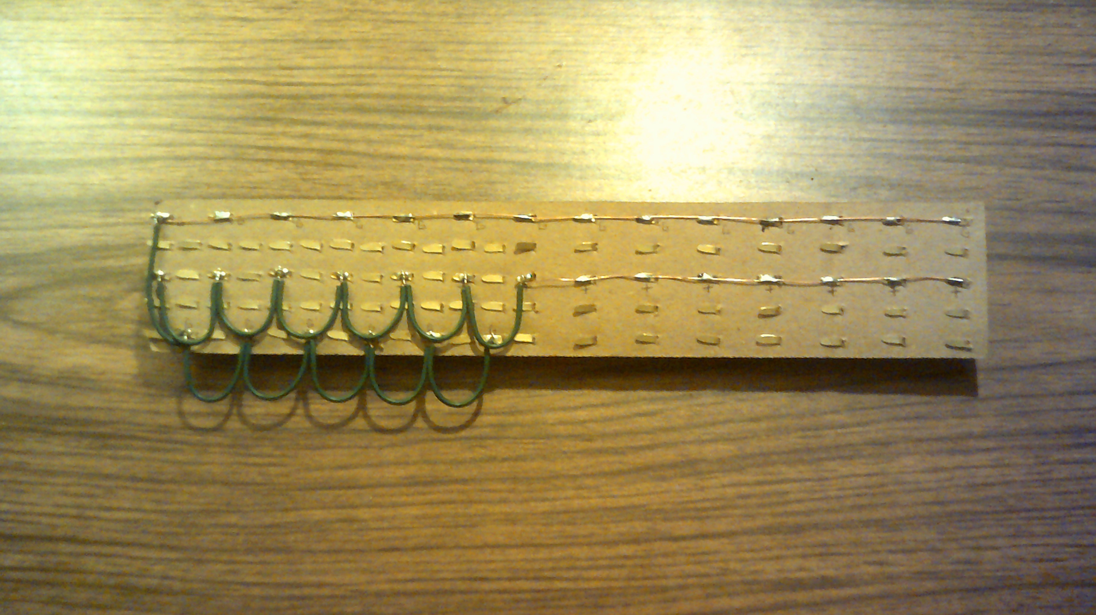
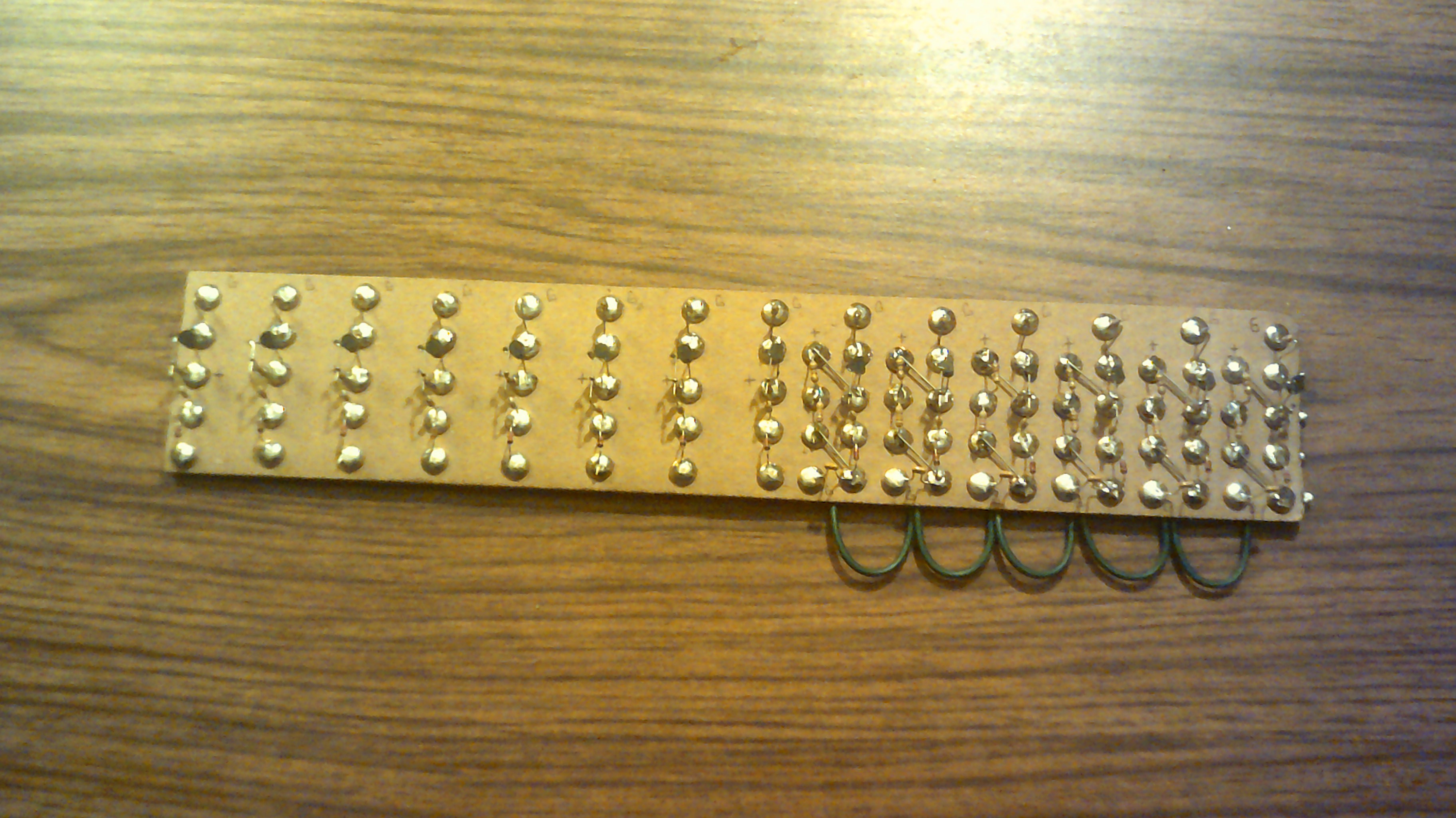
Input switch interface panel
01/15/2017 at 00:05 • 0 commentsThis panel acts as the interface between the input switch panel and the led display panel as well as providing debounce circuits for the six function switches. Power and ground bus on the back of the panel. 14 transistors are Not gates and the debounce circuiit is a very basic RC arrangement that feeds the switch signal to the 6 function Not gates.
![]()
![]()
-
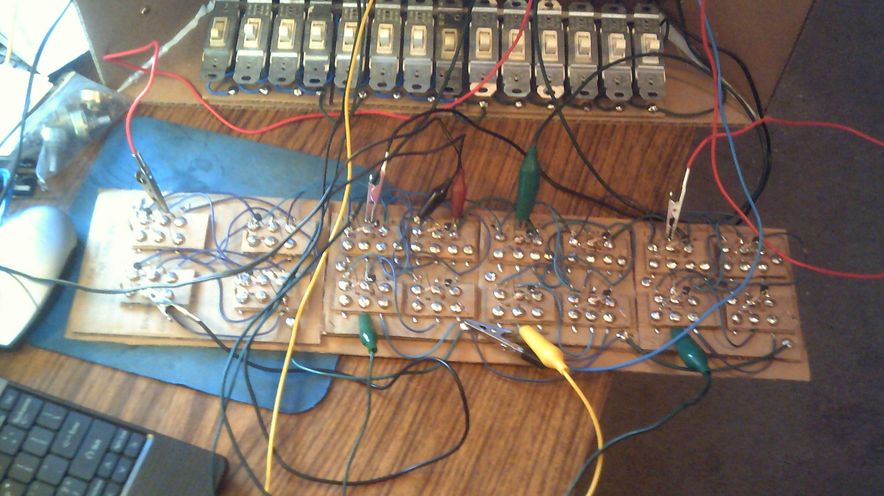
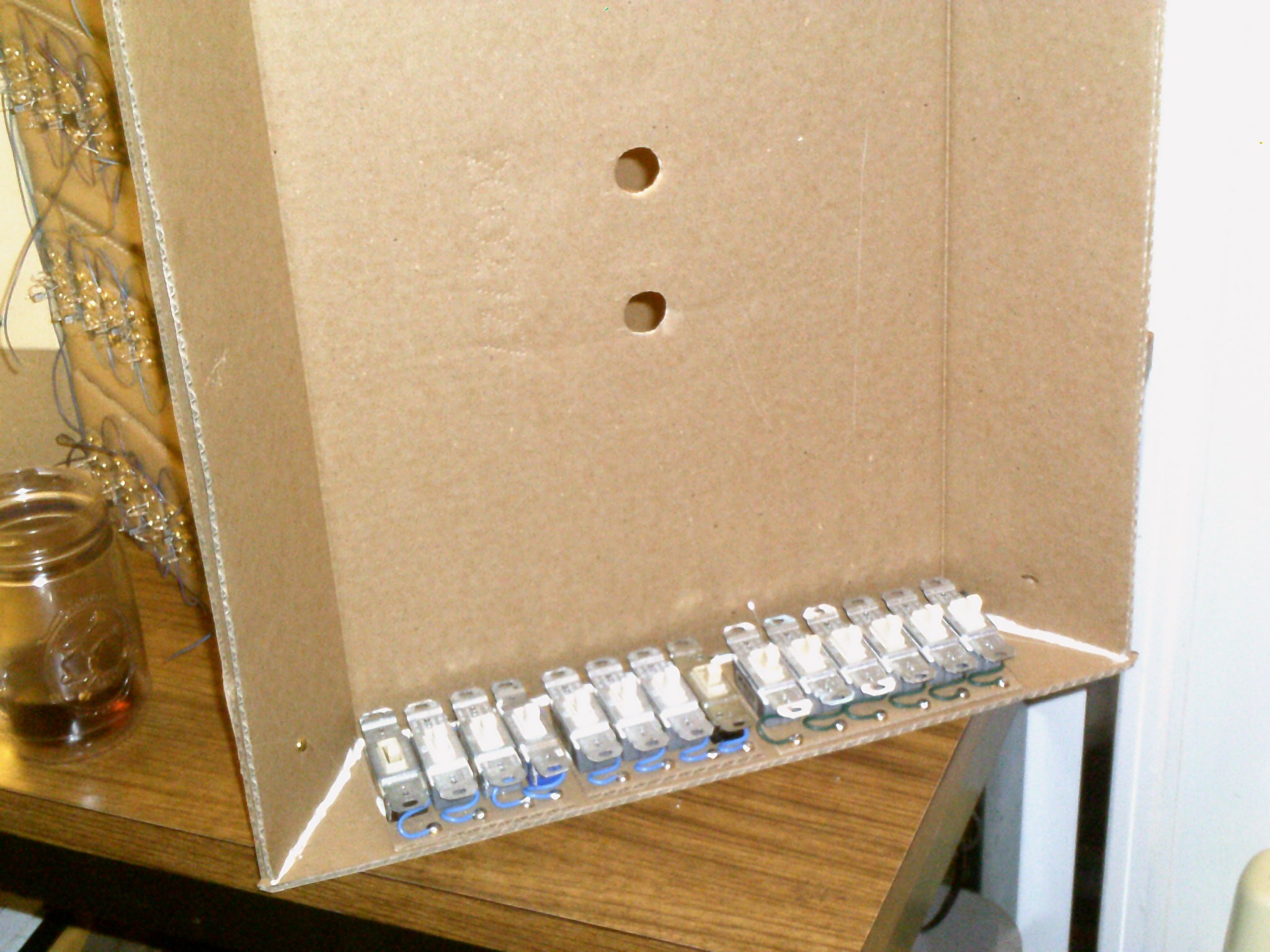
Input panel assembly
01/05/2017 at 09:24 • 6 commentsWell, I have started the layout for the switch input section for this machine. As with my 4-bit adder, I am using household power switches found at the local thrift store. Just a little bit oversized but then again this project is a tad odd anyway :-) The bank of four on the left is address input. The middle bank of four is data input and the right side bank of six is for control functions ( Step, Run, Stop, Reset, Deposit and Examine ).
![]()
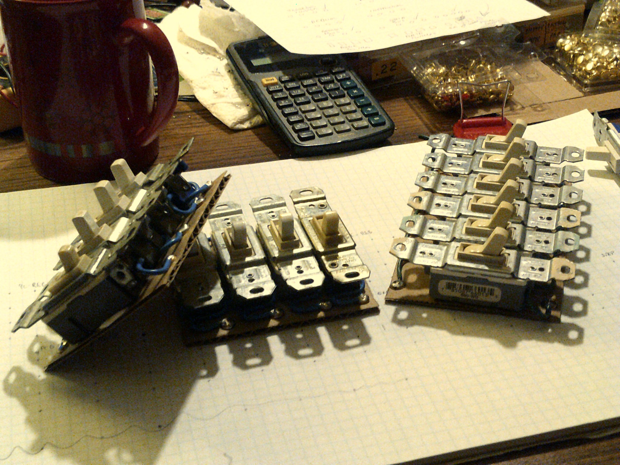
Here is closer look at the switch modules. Again using cardboard as the base material.
![]()
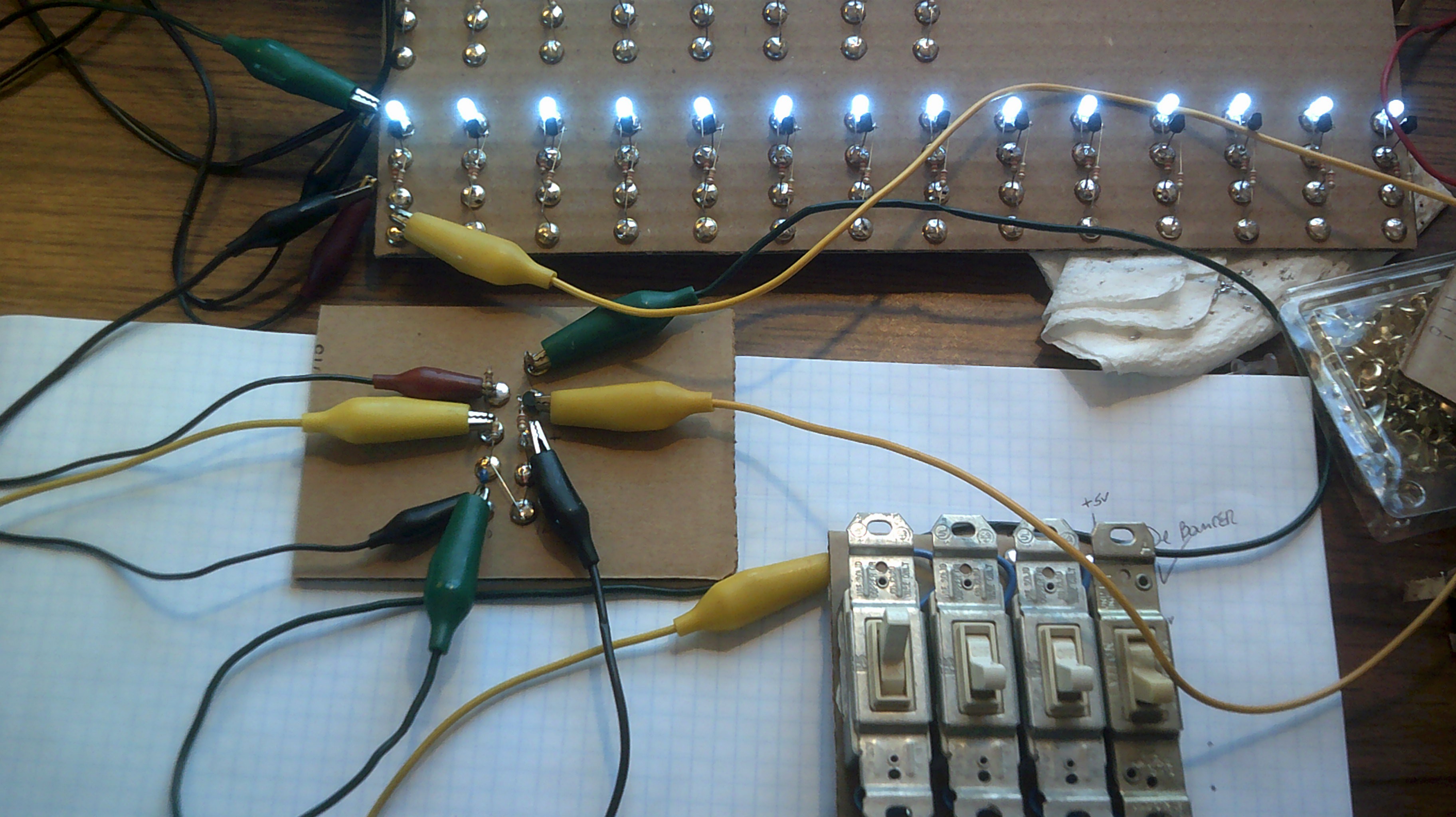
01/09/17 - I have decided on a simple basic RC debounce circuit for the six function switches. So I am laying out a strip with the debouncers and Not gates to be placed between the switches and the lower display led circuits. I am using the Not gates as the led inputs need a solid 0 or 1 to function and the switches are spst and going to ground. I lack a scope to see what my signals look like so my debounce resistor and cap value will be trial and error. Hopefully less error :-) I will post the circuit shortly.
![]()
-
January 3, 2017 - Neat find at thrift store
01/03/2017 at 18:59 • 0 commentsA bit off topic but was at the local Habitat Restore today and came across a TI-30XA scientific calculator for 3 dollars. Not bad when I have been using my Radio Shack credit card sized calculator for more years than I can remember.
![]()
The Cardboard Computer - IO is my name
My goal is a 4-bit CPU using recycled cardboard substrate and Diode Transistor Logic. This is an educational platform for me.