 ChengDanguo
-
1MCU外设(MCU Peripheral)
在正式使用MULIT-FOC之前,你首先需要了解MCU的引脚功能映射,下表给出了引脚功能定义以及用户功能定义:
Before formally understanding how to use muilt foc, you need to understand the pin functions of the MCU. The following table shows the peripheral pin diagrams and pin functions used in the STM32F427 development board:
引脚 引脚功能 用户功能 引脚 引脚功能 用户功能 PB3
PB4
PB5SPI_1_SCK
SPI_1_MISO
SPI_1_MOSITMC4671总线A
TMC4671 busAPB10
PB11I2C2_SCL
I2C2_SDAIMU IIC接口
IMU IIC portPE12
PE13
PE14SPI_4_SCK
SPI_4_MISO
SPI_4_MOSITMC4671总线B
TMC4671 busBPB12
PE10GPIO_EXT12
GPIO_EXT10IIC INT1
IIC INT2PB14
PB15USB_HS_DP
USB_HS_DMUSB接口
USB portPA9
PA10USART1_RX
USART1_TXUART接口A PA13
PA14SWDIO
SWCLKSWD接口
SWD portPC6
PC7USART6_RX
USART6_TXUART接口B PB9
PB8
PB1
PB0TIME4_CH4
TIME4_CH3
TIME3_CH4
TIME3_CH3PWM_1
PWM_2
PWM_3
PWM_4PB6
PB11
PD7
PB15GPIO_output
GPIO_output
GPIO_output
GPIO_outputTMC4671_A_CS
TMC4671_B_CS
TMC4671_C_CS
TMC4671_D_CS显然,与其他开发板类似,你需要熟悉引脚功能映射及其所对应的用户功能,这不会很难。
Obviously, similar to other development boards, you need to be familiar with pin function mapping and its corresponding user functions, which won't be difficult.
你可以在用户程序中用宏定义或函数嵌套将引脚功能与用户功能进行封装,这会提高开发效率。
You can encapsulate pin functions with user functions through macro definitions or function nesting in user programs, which will improve development efficiency.
需要注意的是:开发板采用四线SWD接口作为调试接口,如果你选择的下载器是JTAG接口的,那就需要重新调整接口,如果你对MCU开发熟悉的话,这通常也不难。
It should be noted that: The development board uses a four wire SWD interface as the debugging interface. If you choose a JTAG interface for the downloader, you need to readjust the interface. If you are familiar with MCU development, this is usually not difficult.
-
2SPI通信(SPI Communication)
相信在之前的内容中,你已经不止一次的听到TMC4671这个器件,这对你来说可能是个很新且具有挑战性的内容!
I believe that in the previous content, you have heard about the TMC4671 more than once, which may be a very new and challenging content for you!
没错!该项目的核心就是围绕TMC4671展开的,但幸运的事:你无需了解TMC4671的全部技术细节,就可以轻松地使用!
Yep, the core of this project is centered around TMC4671, but fortunately, you don't need to know all the technical details of TMC4671 to easily use it!
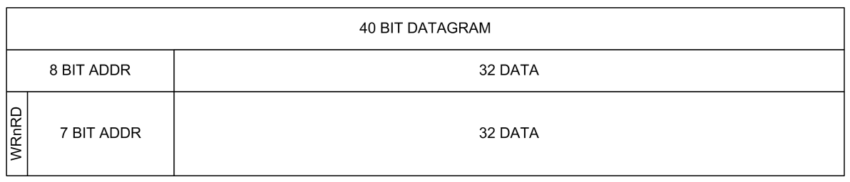
首先,你需要了解有关使用SPI总线与TMC4671进行数据交互的相关知识,下图给出了TMC4671在在一次数据交互中的数据帧定义定义形式:
Firstly, you need to understand the relevant knowledge about using SPI bus for data interaction with TMC4671. The following figure shows the definition form of TMC4671's data frame in a data interaction:
![]()
从上图可以看出,一个数据帧由40个位二进制组成,但对于不同的寄存器类别,又有细微差别:
From the above figure, it can be seen that a data frame consists of 40 bits, but there are slight differences for different register categories:
对于只读或只写的寄存器,其中8位为地址位,32位数据位,这很好理解
For read-only or write-only registers, where 8 bits are address and 32 bits are data, this is easy to understand对于可读可写寄存器,第一位为读/写标记位,7位为地址位,32位数据位,这也不难
For readable-writable registers, the first bit is the read/write flag, 7 bit is the address, and the 32-bit data, which is not difficult.此外你还需要注意SPI工作模式和SPI最大时钟频率,这决定了你是否能稳定、可靠的传输数据,对于TMC4671而言需要满足:
In addition, you also need to pay attention to the SPI mode and SPI clock frequency, which determines whether you can stably and reliably transmit data. For TMC4671, it needs to meet the following requirements:
1、SPI工作模式为模式3,也就是 CPOL = 1 and CPHA = 1;
The SPI mode is Mode 3, which means CPOL=1 and CPHA=1;
2、SPI最高时钟频率小于8Mhz,推荐时钟频率为1Mhz。
The max clock frequency is less than 8Mhz, and the recommended clock frequency is 1Mhz.
上述两个参数由TMC4671器件特性决定,所以无论你是采用的硬件SPI还是软件SPI,都务必要确认在你的SPI初始化程序中的SPI工作模式以及时钟频率这两个参数!
The above two parameters are determined by the characteristics of the TMC4671 device, so whether you are using hardware SPI or software SPI, it is necessary to confirm the SPI operating mode and clock frequency parameters in your SPI initialization program!
-
3寄存器应答模式(Register Response Mode)
接着,你就需要了解TMC4671的寄存器地址及应答模式的相关知识,你无需了解所有的地址及其对应的功能,在之后的说明中我会介绍相对重要的寄存器,通过这些寄存器你可以进行大多数操作,如需二次开发或其他操作,你可以在TMC4671中查询完整的寄存器信息。
Next, you need to understand the register addresses and response modes of TMC4671. You don't need to know all the addresses and their corresponding functions. In the following instructions, I will introduce the relatively important registers through which you can perform most operations. If you need secondary development or other operations, you can query the complete register information in TMC4671.
以下内容非常重要,如果你之前未接触过SPI通信,请必仔细阅读并理解!!!
The following content is very important. If you have not been exposed to SPI communication before, please read and understand it carefully!!!
这有助于你后续的开发!!!
This will help you with your future development!!!
最先需要提前说明的是,TMC4671寄存器的应答模式有两类:一类是直接读取寄存器,还有一类是内地址应答寄存器:
The first thing that needs to be explained in advance is that there are two types of reply modes for TMC4671 registers: one is the direct read register, and the other is the internal address acknowledgement register:
直接应答模式:和STM32的寄存器操作类似,直接向寄存器写入32位数据即可;
The direct read mode: is similar to the register operation of the STM32, and 32-bit data can be written directly to the register内地址应答模式:该模式下的寄存器存在一个唯一的内地址寄存器对其内部功能进行编址,这意味着所有的寄存器读写,你都需要先对内地址寄存器进行写操作,在指定你需要读写的“内地址”后,再对功能寄存器进行操作。这一类寄存器所储存的数据通常为16bit或32bit,由于数据所占空间较大,因此需要采用内地址映射进行扩展编址
直接应答模式是简单的,但内地址应答有些复杂,对么?下面我会着重补充内地址应答的机制:
The direct reply is simple, but the internal address is a bit complicated, right? Below I will focus on the mechanism of internal address response:
对于某个寄存器A,他的外地址是0xNN,假设这个寄存器存放了“器件信息”,你注意到这里打上了引号,这意味着器件信息是一个统称:器件名称、出厂时间、出厂版本都可以归类为器件信息,在寄存器A中器件名称、出厂时间、出厂版本都对应了一个内地址。
For a certain register A, its external address is 0xNN. Assuming this register stores "device information", you noticed that it is enclosed in quotation marks, which means that the device information is a collective term: device name, factory time, and factory version can all be classified as device information. In register A, the device name, factory time, and factory version all correspond to an internal address.
那如何指定内地址呢?
How can I specify an internal address?
对于任意的寄存器A,都存在一个内地址寄存器B,他的外地址是0xMM,寄存器B确定了寄存器A中存放的数据在寄存器A中的地址,比如器件名称的内地址是0,出厂时间的内地址是1,等等。
For any register A, there exists an internal address register B with an external address of 0xMM. Register B determines the address of the data stored in register A, such as the internal address of device name being 0, the internal address of factory time being 1, and so on.
基于上述说明,那么假设你需要在初始化程序中首先读取器件名称以验证是否初始化成功该如何造作呢?如果你理解了内地址应答模式的原理,下面这段伪代码应该不难理解:
Based on the above explanation, what if you need to first read the device name in the initialization program to verify if the initialization is successful? If you understand the principle of internal address response mode, the following pseudocode should not be difficult to understand:
WRITE: 0xMM00000000 =>向寄存器B写入内地址0
READ : 0xNN00000000 =>向寄存器A的0号为读操作作业:你希望将0xFFFFFFFF的数据写入寄存器C的第4个单元中,其中C的地址为:0xAA,内地址寄存器地址为0xBB,又该如何操作呢?
Assignment: How do you want to write the data of 0xFFFFFFFF to the fourth unit of register C, where C's address is 0xAA and the internal address register address is 0xBB?
WRITE: 0xBB00000004 =>向寄存器D写入内地址4
WRITE: 0xAAFFFFFFFF =>向寄存器C的4号位为进行操作好在内地址应答并不常见,这个例子只是为了你能理解,希望它不会干扰你(笑)
Fortunately, internal address responses are not common, this example is just for you to understand, and I hope it won't interfere with you (LOL)
-
4寄存器地址(Register Map)
在本章的第二节中我们已经提到,TMC4671通过至少7bit进行编址,这意味着TMC4671最多有128个寄存器地址!
We have already mentioned in the second section of this chapter that the TMC4671 is addressed by at least 7 bits, which means that the TMC4671 has a maximum of 128 register addresses!
但好在,若只为满足基本使用,其中大多数的寄存器并不需要我们进行操作。
But fortunately, most of these registers do not require us to operate for basic use.
下面让我们来学习实现基本操作所需要使用的必要寄存器:
Multi-FOC: Universal multi-channel FOC controller
A Universal multi-channal FOC controller for robot systems or Multi-motor collaborative control
Discussions
Become a Hackaday.io Member
Create an account to leave a comment. Already have an account? Log In.