-
5 Slot STEbus Backplane rev 1
05/01/2023 at 03:01 • 4 commentsNOTE: This post contains sponsored content.
I finished rev 1 of a 5 slot backplane and sent it to PCBWay who were kind enough to send me some free boards to try out in exchange for a review of the service. Check out the end of this post for info on how they turned out.
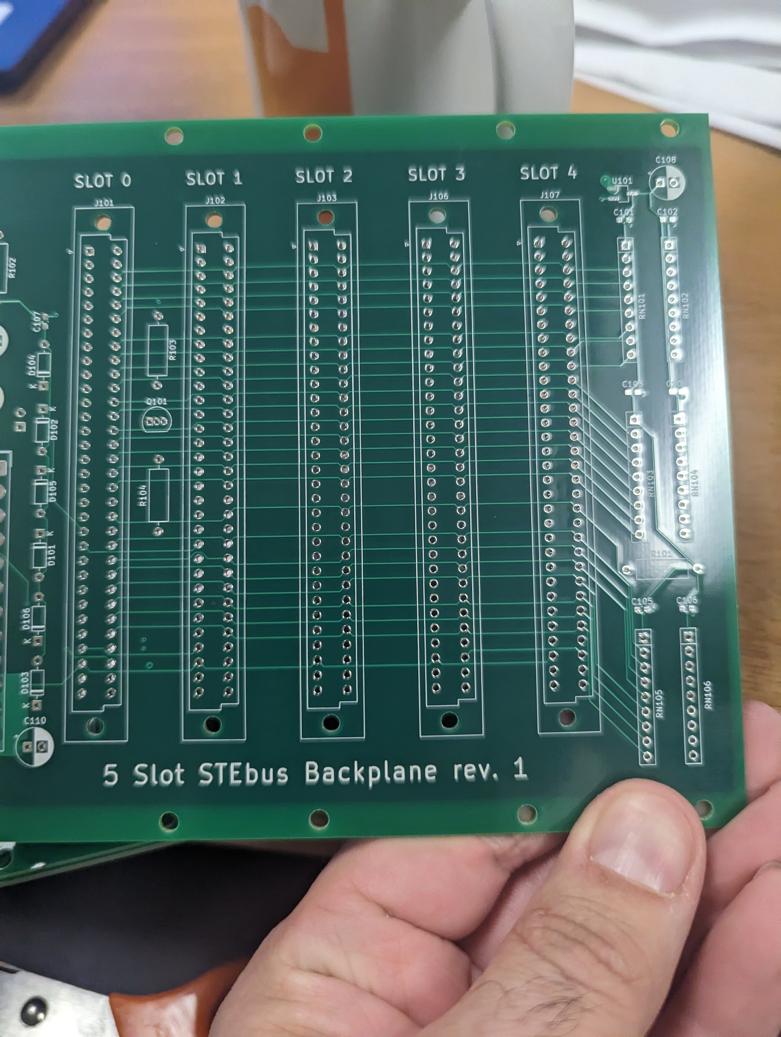
---------- more ----------This is a simple 5 slot backplane with active termination. Follow along with the schematic while I describe the design.
I decided to use an ATX-24 connector to support an ATX power supply since these are very common and fairly inexpensive for multiple power rails. The 3.3v isn't used but the +12v, -12v, and +5v rails provide power for the STEbus rails. The caveat is that the ATX standard defines a looser standard for voltage stability on the +/-12V rails than the requirements for STEBus so the rails may not be compliant. STEBus requires +/-5% and 50mV pk-pk ripple on all rails and -2.5% on the +5V rail. ATX only requires +/-10% on the -12V rail and 120mV pk-pk ripple on the +/-12V rails. In reality, these are the worst case specifications and most ATX supplies will be more stable and have less ripple. Also, a lot of STEBus cards should also work fine with the looser specifications with the possible exception of DAC/ADC cards and the like. The ripple can be further mitigated with more filtering and bigger caps on the backplane or boards. This should also help with voltage drop on the -12V rail. In short, there should be no problem getting a mostly digital hobbyist system running with an ATX power supply.
ATX power supplies use hard and soft switches for power. The backplane includes a header (J104) to accommodate a soft switch but this can be bridge with a jumper or solder bridge to force the soft switch closed. In addition, an ATX supply has a +5VSB rail which is a 5V rail with lower current capability and looser stability requirements. It's meant to supply power to circuits used for the soft power capability and some other standby capabilities like status LEDs. We can tie it to VSTBY on the STEBus and treat it like a battery. This allows us to simulate a power fail by turning off the supply with a soft switch. The full system can be turned off with the hard switch on the power supply. There's a jumper pad (JP102) to tie VSTBY to either +5V or +5VSB.
The other jumper (JP101) ties the PWR_OK line on the ATX supply to ATNRQ0. It is pulled low after power is turned on to give it time to stabilize. It can be used to trigger a power failure interrupt on the line suggested by the STEBus spec. After looking at the schematic of rev 1 I believe there's an error. There's an inverter connected to the line to switch to inverted logic but re-reading the ATX spec I think this is already inverted logic so if you use this revision you might not need to populate Q101, R103, and R104 and jumper JP101 pin 2 directly to Q101 pin 3. If this is the case I'll put out rev 2. Another change that might be worthwhile for rev 2 is the ability to jumper PWR_OK directly to the System Controller board so it can be used to manage SYSRST on startup. Stay tuned for updates.
Bus termination is based on the IEEE-1000 §7.7 Termination Networks. The circuit is verbatim from Figure B.1 Bus Terminology Arrangement with component types chosen from jelly bean parts. A 1N4148 silicon diode and some SD103C Schottky diodes. You should be able to substitute any of these with just about any diodes you have on-hand provided they can handle the current. The 2.8V needed for termination is created with an RT9080 LDO regulator. I happen to have some around from another project and they are more than capable of providing a stable 2.8V. Similar devices should work ok if you have something around but YMMV.
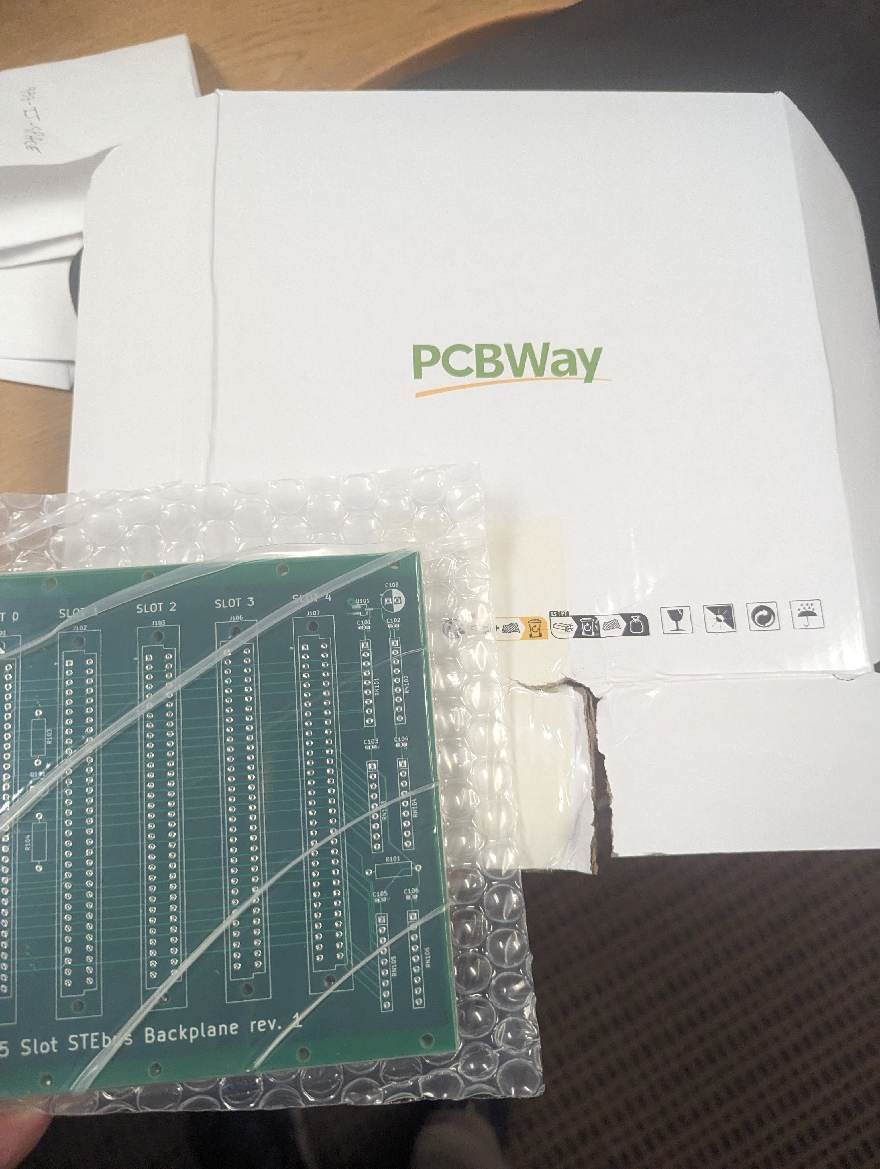
The boards arrived from PCBWay in a timely manner and they were very well packaged.
![]()
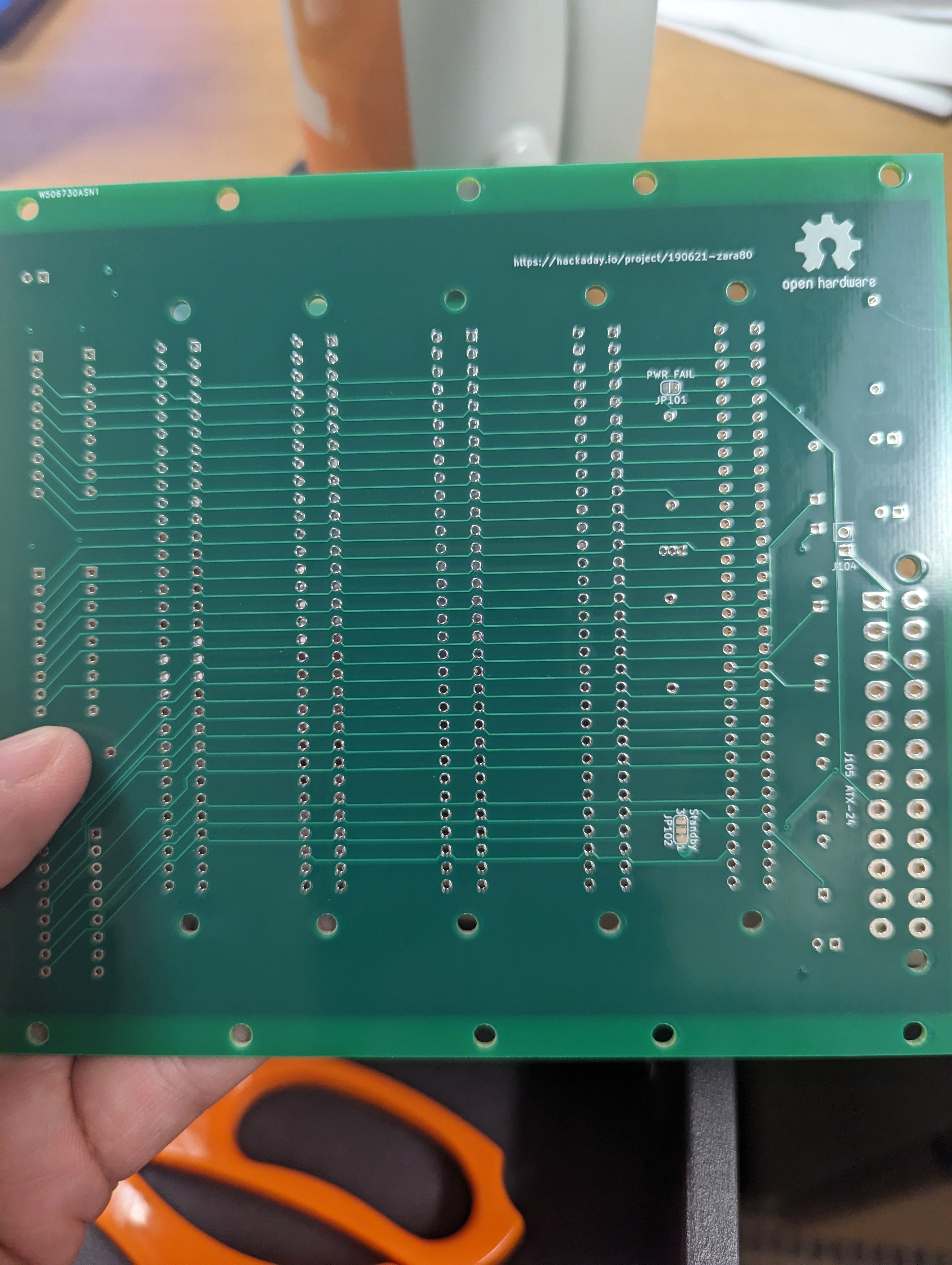
The layout is fairly simple, rev 1 gerbers are available in the github repo. Once I've tested everything, I'll release them here as well. The cost was a bit more than I'd pay at some other PCB proto services but the number of options available for impedance controlled boards and other advanced options is quite a bit larger than those other services and the quality seems to be at least as good as, or better than the others I've used. I'm pretty happy with the boards and I'll definitely use PCBWay again, at least for my HAM radio projects that require impedance control. I'll be ordering the rest of the boards for this project as well.
![]()
![]()
-
Finalized on Bus
04/26/2023 at 16:23 • 0 commentsI began laying out my modified RC2014 bus and I realized it has more problems than just missing signals. There's not termination, layout is not friendly to cross coupling concerns, etc. It's a great breakout for a z80 but it's a badly designed bus for a backplane based system so I'm entirely dropping it. However, I have a better solution.
---------- more ----------While researching some of these issues I ran across STEbus. I'm somewhat surprised I haven't run into it earlier. It's got a lot going for it:
- It's a proper standard. IEEE1000 to be specific. (latest rev seems to be 1988)
- It's designed to be processor agnostic so it's not just a breakout for a specific processor's pins.
- It was quite successful in its day and there are many industrial automation modules available
- The physical layout is based on eurocard (STEbus means STandard Eurocard bus). It supports 3U and 6U 160mm cards and uses the standardized DIN 41612 plug and socket. This means subracks and cases are plentiful and easy to find.
It's essentially an 8-bit version of the VME bus designed to reduce costs when 8-bits are enough. (often the case in industrial automation settings) It never really caught on in the homebrew computer world because it came a bit late when ISA was already dominating with the IBM PC and clones. It's a shame because it's really a great bus for the purpose. There are some homebrew computers using the bus and a lot of the industrial systems are useful too including a variety of CPU boards (z80, 6809, 68000, etc.), serial boards, etc.
One of the design goals of the bus is to make it very easy and inexpensive to create peripheral cards for STEbus. It puts most of the tricky arbitration logic on the System Controller card (often a CPU card) so peripherals typically just need some basic logic, buffers, and address decoding.
I'm attaching the relevant standards documents to the project but I'll summarize the important parts in this post.
The physical layout uses 100mm (3U) x 160mm eurocards. 6U cards are allowed but not suggested. This small size decreases cost and encourages separation of functions onto different cards. There are a few classes of cards to will different roles.
- System Controller - This is a required and there should be only one. It generates the system clock, system reset, and transfer error signals. This can be a separate card or it can be combined with another card. Often this is part of a CPU card.
- Arbiter - This handles allocation grants for masters. The STEbus allows multiple master cards (usually CPUs but can also include DMA sources) and the arbiter decides which gets to control the bus. Like the System Controller, this can be on a CPU card.
- Master - This is a card that can control the transfer of data on the bus. This is usually a CPU board or a DMA controller. There can be a special Master call the Default Master which automatically gets control of the bus until it releases control. A Master can be Release-On-Request (the Default master is always RoR) or Release-When-Done. A Default Master does not need to be present and if one isn't, the Arbiter will choose a current master.
- Slave - This includes all boards that can only receive and respond to bus transfers. Most peripherals will be Slave cards. A card can act as both a Master and a Slave.
The STEbus is asynchronous and uses various synchronization and attention lines to sequence data transfers.
A CPU card can use off-card memory but is limited to 1 MiB due to the 20-bit address space of the bus. A paging system can be implemented to address more memory or a CPU card and contain more memory which isn't accessible over the STEbus. In addition to memory, the bus allows for 4 KiB of I/O addresses for CPUs which have I/O ports (like the Z80).
The bus does not differentiate between DMA requests, interrupts, and similar functions but instead provides 8 attention request lines. These can be used for DMA, interrupts, and similar functions such as notifying of an imminent power failure.
Electrically, there are 2 power buses available. A +5V bus with a maximum available 4A per card. This is intended to be the primary power for all cards. In addition, +12V and -12V buses are provided at a maximum of 1A per card. These have looser noise requirements and are intended for RS-232 signaling, bipolar OPAMP rails, etc. Finally, an optional +5V battery bus is available at a maximum of 1A per card. This connects to a battery backup or UPS and is intended for critical components to function in the event of a power failure. It may be tied to the main +5V bus if a UPS is not available.
There are a few STEbus projects on hackaday including this one which contains links to a lot of STEbus cards and some great information on the bus itself.
-
RC2014+VW Bus
04/17/2023 at 17:14 • 0 commentsThe bus I'm using is based on the RC2014 bus. It's primarily a break out for the Z80 pins with a few notable changes.
The biggest change is the use of a JAE TX-24/25 connector instead of 2.54mm headers. The RC2014 boards suggest not using pins 40 and 80 as the resulting board would need to be longer than 100mm (the magic width for using the free version of some PCB design tools and the limit for super cheap proto boards from many manufacturers). These were used because they are very easy to hand solder, most hobbyists have a bunch of them in junk boxes, and they are very inexpensive. I've decided to move to the TX-24 connector a it is 1.27mm pitch so 80 pins fit very easily on a 100mm board with plenty of room to expand with another connector if needed. They are keyed, shrouded, and click together leading to a fairly robust connection and can be plugged and unplugged a number of times. They are also fairly inexpensive at just over $2 per connector in lots of 10.
The RC2014 extended bus does not connect pins 41-56 and uses them as a way to key the 2.54mm header connectors. My bus connects these to GND since they are already present, this should help with impedance and noise issues that can arise with longer runs of the RC2014 bus while remaining compatible with the pinout.
There are a number of user pins reserved in the RC2014 bus. My bus uses 5 of the 8 to add some important strobes from the S-100 including pSTVAL, pSYNC, ERROR, POC, and INTA. These are defined as in the S-100 specification. Certain RC2014 boards use these for other signals causing incompatibilities but this is a problem with user defined signals regardless of their use. Care should be paid when adding other boards.
I'm ignoring DMA and temporary master capabilities of the S-100 as well as 16-bit data transfers. If I decided to add this later, I'll likely utilize pins 41-57 or add a second connector to the bus.
I haven't added additional power rails as the occasional +/-10v (for RS-232), etc. can be easily generated on-board with modern DC-DC converter chips. The RC2014 does not state, but assumes a regulated 5v rail which is reasonable for a small system. 5V LDO regulators (for example, the 1117) are cheap and easy to use to increasing the rail voltage and regulating on each board is not a bad idea. For now, I plan to add a footprint for a regulator but not populate it. If necessary, I can add the regulators and increase the rail voltage to 12v or so.
-
Introduction
04/17/2023 at 16:28 • 0 commentsThis is a homebrew Z80 based retroish computer that I'm designing and building. This post provides some background on why I'm working on this project, how I got to the design, and what my end goals are.
---------- more ----------Why am I building another Z80 based retro computer? This one is easy. I'm old enough that I cut my teeth on early home computers in the 1980s. I started with an Apple //e and moved on to an XT clone but I never had one of the classic S-100 based systems. There are many options today for one of these including purchasing an original Altair or IMSEI, building a clone, or using a modern work-alike system like the RC2014. I wanted to learn all I can about the details and design considerations so I opted to create my own system from scratch. I'd like it to work with classic or modern modules in case I decide to pop in an old 8" floppy, etc.
One of the design requirements is to stick with the general feel and soul of a classic S-100 system but not limit myself to original components which can be tough to find and sometimes expensive. I'm using modern CMOS components, denser memories, etc. while still keeping the overall design features of the classic hardware. I went with a CMOS Z80 since you can buy them new but the architecture is essentially the same as it was in the '70s. The CMOS is more tolerant to noise on the bus and has higher fanout than the NMOS devices. The modern Z80s can also run at higher clock speeds.
Next I had to decide on a bus. Since I've building most of this myself, it doesn't matter as much as if I'd planned to use existing modules from the start. Originally I was going to stick with S-100 but there is a lot of glue logic needed to put a Z80 on an S-100 bus, mostly because the bus originally coincided with the pinout on the 8080. There are also a lot of pins used to allow for temporary bus masters and DMA, functions I'm not interested in implementing this time around. The next obvious choice is the RC2014, a bus designed to get a Z80 system running with minimal effort. It is a breakout of the Z80 pins with power. However, it has a number of problems, it's not well designed from a robustness standpoint. It's not designed for latching of address and data values, it has only one (or two in the extended version) ground pin, it only has 5V lines, lacks multi-level interrupts, and isn't laid out with signal integrity in mind.
After spending too much time thinking about and designing for S-100 I wanted to get something done so I switch to RC2014 with a few changes I'll detail in another post.
In addition to a CPU board with a ROM chip, I'm creating a RAM board, a dual serial board with a PC16552 compatible UART, a front panel/debug board, and some sort of TBD storage (likely an SD card simulating a floppy). User I/O will be through a VT420 terminal.
 Trevor R.H. Clarke

