Clyne
Clyne-
First draft of Guide released
10/08/2023 at 22:15 • 0 commentsTo help users get acquainted with the DSP PAW system, I've been putting together a guide that covers hardware setup and shares a few algorithm examples that demonstrate how to use the user interface.
The first draft is done, including four algorithm examples: pass-through, user-controlled attenuation, moving average, and differentiation. Everything from signal generation to output observation is done through the DSP PAW system -- no external lab equipment needed! More algorithms will be added in the future, along with extra documentation on how to use other available features. This guide ultimately aims to be the one document needed to turn a new user into a DSP PAW expert.
You can download a PDF of the guide here. The editable document (.odt) version of the guide is available on the repository.
-
Firmware overview
10/08/2023 at 22:03 • 0 commentsMost of the previous project logs have focused on the DSP PAW hardware and using the system and user interface to test algorithms. However, the firmware that makes this project possible is just as significant as these other portions and deserves just as much documentation. I have just added some documentation to the source code to start, but I will also take this log entry to go over the main components of the firmware and how they work together to get things done.
C++
The firmware is written in C++ rather than C. Using C++ actually makes a lot of sense for embedded systems so long as you avoid dynamic memory allocations and some other higher-level features (unless you have made the needed accommodations in your firmware). Classes and objects can neatly package data and functionality together, principles like Resource Allocation Is Initialization (RAII) can make code flow more concise and safe, and compile-time variables or functions can save on precious memory space.
Even simple features like the "auto" keyword just make your code easier to work with. With the growth of C++ both in general and specifically in the embedded domain, there are less and less reasons to make the change if you are still stuck on choosing C.
Real-time operating system (RTOS)
The DSP PAW firmware is built on top of an RTOS which provides the functionality to execute multiple services "at the same time", facilitate communication between these services, and guarantee as best as possible that code will never run behind schedule. "At the same time" is in quotes since the vast majority of microcontrollers are single-core, meaning that simultaneous execution is achieved by switching between different services or execution states at a milli- or micro-second scale.
The RTOS used for DSP PAW is called ChibiOS. This RTOS has spectacular support for STM32 microcontrollers, is available as free software under a GPL license, and has a great community that contributes extra hardware support and other bits of functionality. It's worth checking out if you have not heard of it before.
DSP PAW uses ChibiOS to run multiple services (threads) at once:
- Conversion manager: Manages the ADC and DAC for signal conversions as well as the unprivileged algorithm execution thread.
- Communication manager: Watches for USB communication and handles incoming commands accordingly.
- Monitor: Monitors hardware status, uses the add-on board's LED to indicate this.
These threads use either "mailboxes" or service classes to send messages to each other when necessary. When none of the threads need to be active, ChibiOS enters an idle thread that allows the microcontroller to sleep.
Unprivileged (and safe) execution
The algorithm execution thread is unprivileged, meaning it is restricted in its ability to access certain registers or functions. Additionally, a hardware memory protection unit is used to prevent this thread from reaching beyond the memory it is allocated. Finally, a service call routine is made available through the RTOS to allow the algorithm access to just the few firmware functions that it needs to process data (e.g. large trigonometric functions, parameter knob reading, etc.)
This stack-up of protection keeps the firmware safe from user-loaded algorithms that misbehave. If an algorithm does something that it shouldn't, one of a few handler functions will be executed to clean up the mess, unload the algorithm, and notify the user that something has gone wrong. This means you can continue to use your DSP PAW hardware without needing to reset the microcontroller or worry about bad code causing unintentional damage.
Hardware abstraction
ChibiOS (and most other operating systems) include a hardware abstraction layer (HAL) so that your top-level code can avoid worrying about the nuances of your specific microcontroller and peripherals. By using ChibiOS's HAL, the firmware becomes much easier to port to other microcontrollers or development boards. At most, the programmer will need to handle some I/O pin numbers, the configuration structures and memory buffers for the ADC and DAC, and a couple of assembly instructions; the rest of the firmware is entirely independent of current choice of microcontroller.
Algorithm uploading
DSP algorithms designed by the user are compiled with a regular C++ compiler (GCC) to create an ELF binary. The ELF format is a common standard -- most Linux programs are compiled to this format. The algorithm ELF binary contains all of the user's code and has its entry pointer set to the start of the algorithm (the process_data function).
This binary is uploaded in full to the microcontroller over the USB connection. From there, the binary is parsed and prepared for execution: the entry pointer is saved, memory and variables are initialized, and code is copied to the memory address that it expects to execute from. When it's time for the algorithm to execute, the unprivileged thread simply makes a call to the entry pointer.
If the algorithms needs facilities from the C++ standard library, the necessary functions are compiled into the ELF binary by the user interface. Larger functions and firmware utilities like reading the parameter knobs are accessed through ARM service calls.
USB Communication
The firmware uses ChibiOS's serial USB driver to talk with computers and the DSP PAW user interface. "Serial" may make you think of UART and slow data transfer rates like 9600 baud; however, the driver takes full advantage of USB speeds to maximize data transfer without any complicated configuration.
Commands from the user interface control the hardware and either send or receive chunks of sample data. For simplicity, commands are identified by a single letter with additional parameters or data following if necessary. There may be some value in making this system more robust by using checksums and packet structures, though there have been no issues in communication due to this minimal format.
Signal data management
Processing signals in real-time requires a lot of care. To keep a continuous stream of data flowing, the input and output signal buffers are split in half: while one half is being streamed into or out of the microcontroller, the other half is being processed by the algorithm. A "SampleBuffer" class manages the firmware's split buffers and tracks the most recently modified buffer so the algorithm executor knows what memory to work with.
The firmware for the DSP PAW hardware is available here on the project's repository if you would like to take a closer look.
-
Schematic revision
09/23/2023 at 19:23 • 0 commentsThe latest iteration of the add-on board saw a major step towards a final design that I would feel comfortable selling to interested users. As previous project logs have shown, the design still had numerous component substitutions and circuit rewirings to be made. Since the board's circuits were all brought to an acceptable state I have added these fixes back into the schematic. With a couple of other design changes, I have arrived at (what I truly hope will be) the final add-on board design that is production ready.
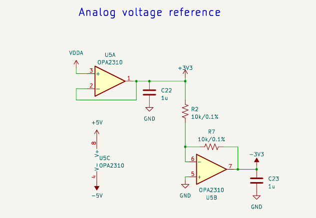
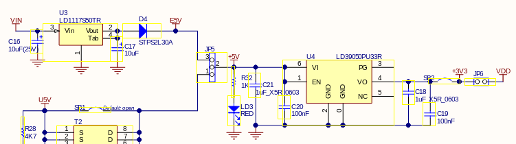
Analog voltage reference
Despite the effort that has gone into bringing a high-accuracy 2V reference to the add-on board, I am making the decision to return to relying on the NUCLEO's provided 3.3V reference. Firstly, this will eliminate the requirement of removing (desoldering) a jumper resistor from the NUCLEO board. Second, a closer look at the microcontroller's documentation reveals that VDDA should never be less than VDD, meaning the use of a 2V VDDA is technically unsupported (although it has worked well for the prototypes).
As a final solution, the NUCLEO's provided reference will be buffered to prevent sagging from the add-on board's load. We will also generate a negative reference voltage for use with the input signal circuit; this should both improve input accuracy and prevent the ADC input from exceeding its specified range.
![]()
Input signal circuit
In the last design iteration the input signal path produced an unstable, oscillating output that required multiple changes to fix. It is still unclear what resistance is driving the second stage's attenuation factor as well as the overall stability of an inverting amplifier with gain less than one. I've redesigned the input path entirely to create a circuit that is well-defined in its behavior:
![]()
The first stage has been modified to use the same Sallen-Key architecture as the output amplifier circuits. The slight loss in performance is outweighed by the reduced design complexity and the non-inverting output that makes the revised second input stage possible. This second stage uses a surprisingly simple voltage divider to achieve both the desired attenuation and offset to the positive voltage range: the lowest input voltage of -3.3V becomes 0V, the midpoint of 0V gives 3.3V/2, and the maximum of +3.3V remains at 3.3V. A buffer takes the result through a final low-pass filter that was added during testing before entering the ADC.
Other changes
Apart from these two major changes are the small fixes I made during the prototype testing to stabilize the output signals and a fix for the parameter knobs to use the proper source voltage. I am also switching the two output circuits to use individual amplifier chips; this way, the amplifiers can remain close to the pins that the signals originate from which minimizes noise being picked up by long traces.
The revised schematic is currently available on a "rev2" branch of the project's repository. I have a lot of confidence in this new design, and look forward to testing it out once I finish its layout and order a few prototype PCBs.
PS: Self-assembly
This time around I may also do component assembly myself to both save on cost and to order parts directly from Digikey where I can ensure I get the exact components in my BOM. When I ordered assembled prototypes through JLCPCB, I had to make compromises on component values, tolerances, and even an amplifier choice to make use of the their available stock. By ordering components myself, I'll make sure the resulting prototype is designed exactly to what the schematic calls for.
-
Production and classroom feasibility
09/23/2023 at 18:45 • 0 commentsThe primary audience for DSP PAW is the engineering classroom, where students taking a course on digital signal processing will be using DSP PAW for laboratory or homework assignments to study algorithm design. As the project has grown over the past few months, I now have a better idea of how practical it is to reach this target of classroom use. There are two main factors to consider: cost of the hardware/software and availability of educational material to build a course off of.
The cost of DSP PAW is intentionally minimal. By being open-source, there is no need to purchase software. By limiting hardware to an Arduino-compatible add-on board, we avoid competition with other development boards used in engineering curriculum. Many microcontroller courses already use STM32-based boards, meaning the NUCLEO board this project uses is either already available to students or could be easily transitioned to by those other courses. The outcome is additional microcontroller experience for students and reduced hardware cost for schools.
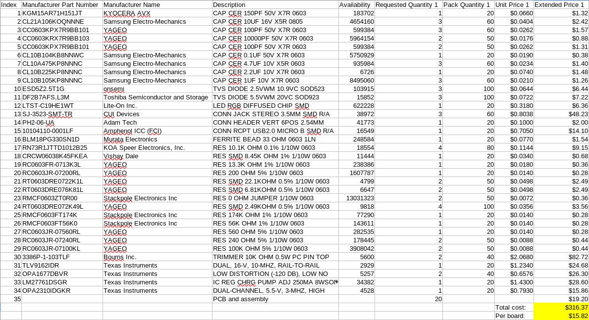
With the add-on board design reaching its final stage, we can make a good estimate on this hardware cost for a classroom of around 20 students. I used Digikey's myList to create a bill of materials for 20 add-on boards, adding an extra line for the cost of the PCB and assembly. The grand total came out to $316.37 USD or just $15.82 per board. This should be a minor expense compared to the "course fees" in the hundreds of dollars that undergraduate engineering courses can often come with. Including the cost of a NUCLEO if necessary only adds $14.60 for a total of around $30 per student.
![]()
Add-on board BOM estimate The greater challenge for this project then becomes providing enough educational material to convince professors to adopt this solution. At the moment we offer multiple code examples to show how topics like convolution, FIR and IIR filters, differentiation, and amplitude modification can be implemented. Tools in the GUI can be used to study algorithm optimization at the CPU instruction level. I'm also writing up a guide to walk through using the software with some of these examples that will be made available in the coming days.
Despite all of this content and documentation, the project is still missing a concrete course outline or some complete laboratory assignments that could truly drive a course. This task will most likely need to wait for an enthusiastic professor that is willing to build up their course around DSP PAW -- something I would certainly be glad to help with. Until then, my plan is to make the add-on board available for anyone to purchase and to see where the project can grow from there.
-
PCB Part 3: Analog output testing
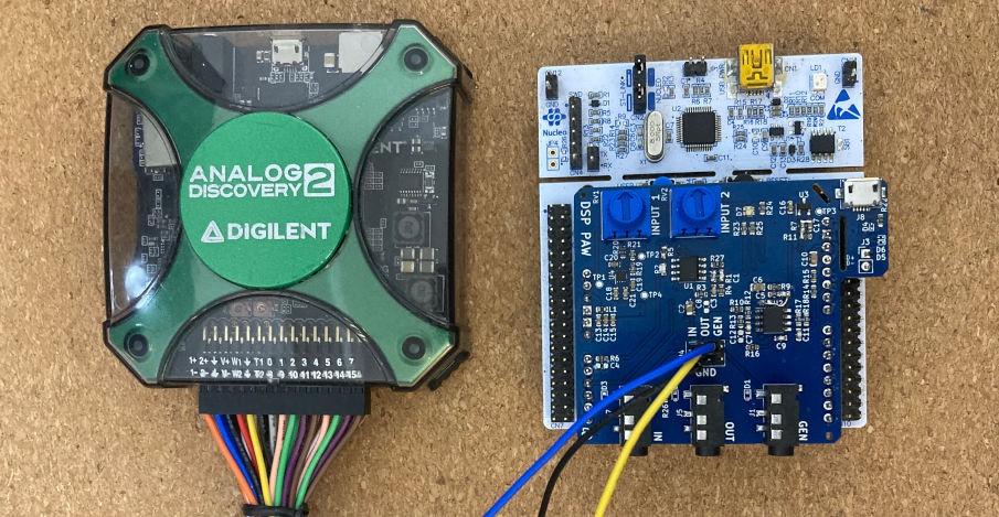
09/04/2023 at 16:23 • 0 commentsWith the input signal circuit figured out, it's time to move on to the output circuits. There are two, one for the algorithm output and another for the signal generator, though both use the same exact circuit. This means we can just test the signal output and copy any necessary changes over to the generator circuit.
For these tests, I used the Analog Discovery 2 again to provide an input signal and oscillator probe for the signal output pin. The development board will be used with the DSP PAW user interface to execute a "pass-through" algorithm that simply outputs the received signal. If all goes well, the oscilloscope will show matching input and output signals (though the microcontroller's sampling rate will introduce some visible steps in the output voltage).
![]()
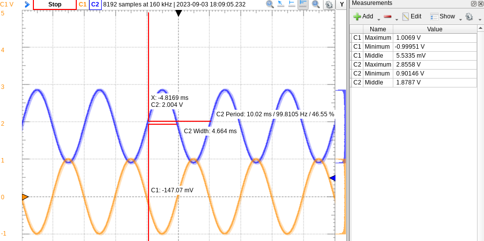
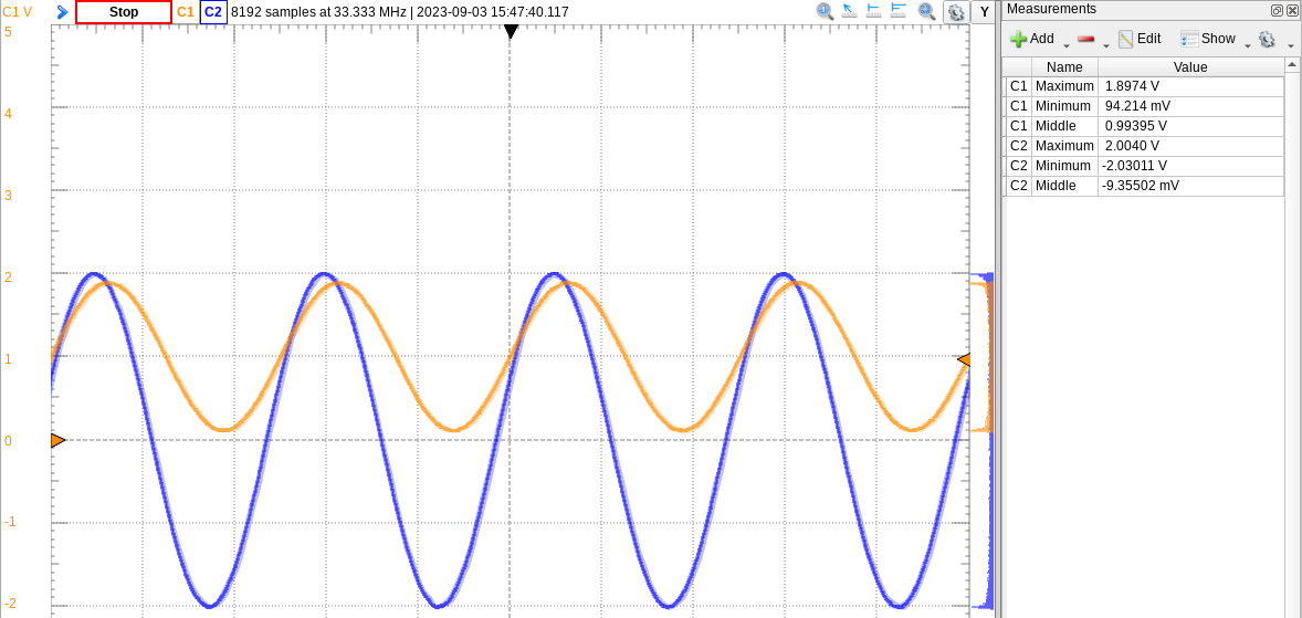
Test setup, with waveform generator (yellow) as a signal input and a probe (blue) on the output. My first test used an easy 1V, 100 Hz sine wave, shown below. The output signal (blue) is surprisingly clean, though it's offset by nearly one Volt. There is a DC blocking capacitor directly on the microcontroller's DAC output, so the offset should not be there...
The signal may appear to be inverted, but that's just coincidential. Processing the signal introduces latency that can create this offset; the opamp's filtering may also cause a change in signal phase.
![]()
Orange: Input signal. Blue: Add-on board output. We'll take care of the offset soon, but first I was skeptical of the output's clean performance. I changed the input signal to a square wave, creating impulses that had a better chance of causing noise or oscillations.
![]()
Orange: Input signal. Blue: Output signal. Those shaded blue areas are spots of noise caught by the oscilloscope. From here, we increase the input signal frequency and zoom in to see some pretty nasty impulses (see below). The output signal is not perfectly matched to the input, but that is just a result of our limited sampling rate.
![]()
Orange: Input signal. Blue: Output signal. To fix up this output, we'll go back to the incorrect offset first and then handle the impulse response.
Output signal offset
Again, we have a DC-blocking capacitor at the beginning of the output circuit, so any offsets should get absorbed and leave the signal centered at 0V. I took a probe to both sides of this capacitor: the microcontroller-side of course had the DAC output with its 1V offset, but when I switched to the other end of the capacitor, the signal began making its way down to 0V just as we wanted.
It turns out the capacitor needs some kind of minimum load on it (like an oscilloscope probe) to allow its charge to settle the output at 0V. Further testing found that a 100 kOhm resistor could do the same trick, and the board may be redesigned to accommodate one.
![]()
Touching a 100 kOhm through-hole resistor (grounded via the USB's shield) to the DC-blocking cap (C6). The circuit's response to offset is quick now, and fairly accurate:
![]()
Orange: Input signal. Blue: Output signal. Fixing impulse oscillation
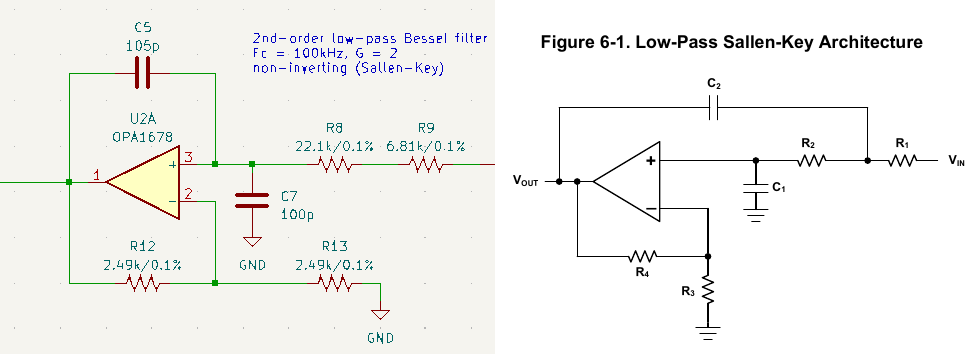
Now it's time to clean up the signal. The strange thing about this issue is that the chosen filter design, a Sallen-Key Bessel filter, should not be creating any overshoot at all. This led me back to the filter design application note I worked off of, reviewing the design process with the circuit on the add-on board.
...and something came up. Here is a side-by-side picture of the board's circuit (left) and the application note's design (right):
![]()
Left: Add-on board's filter design. Right: Filter design from Texas Instruments (SLOA049D). These are not the same circuit, ugh. I attached the feedback capacitor (C5/C2) to the opamp's non-inverting input, instead of between the two input resistors. I have strong confidence that this is our problem.
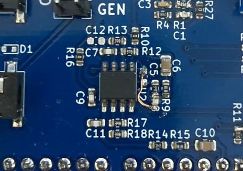
To test this, I removed C5 from its pads and soldered one end of the cap to R8 (where R8 connects to R9). I used a small enamel-coated wire to get the other end of the capacitor re-connected to the opamp's output through its pad on C5.
![]()
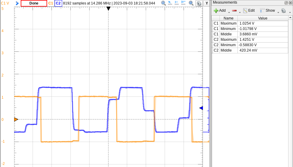
Relocating C5's capacitor to connect to R8, with a wire bringing its other end back to the opamp output. Now we return to the oscilloscope and hope for good results...
![]()
Orange: Input signal. Blue: Output signal. Perfect! Now we've learned that impropely-designed circuits will lead to bad results :)
I'll go ahead and edit the add-on board's schematic and layout to include this fix, so that future boards are wired correctly. Copying this fix to the signal generator would be worse, with its feedback cap (C9) far away from the two involved resistors (R14 and R15). I'll at least make the edit to one board to confirm the circuit is okay otherwise.
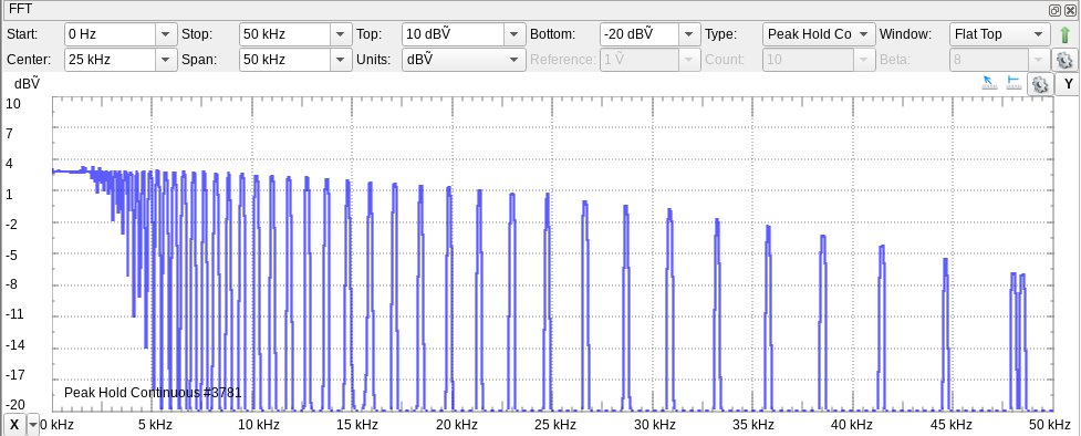
Frequency response and noise analysis
With the circuit fixed, we'll do a frequency sweep just as we did for the input signal path to confirm that signals within our sampling range are not too diminished.
![]()
Frequency response of the output circuit, with a -3dB drop around 25 kHz. The decline toward higher frequencies is more steep, but that can be expected with a sampling rate of 96 kHz. At just 48 kHz, the microcontroller will see the input sine wave as a square wave since it will only capture two samples per period. The output signal stays above -3dB compared to its 0 Hz strength until around 25 kHz, allowing us to work with audio signals well. This range of performance is definitely adequate for educational work.
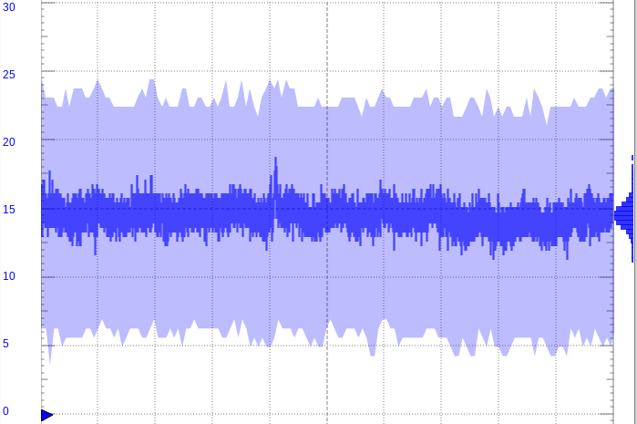
Finally, I took some close-up captures of the output of the input and output circuits to check on signal noise levels. The output path was tested first, proving itself to reliably reproduce signals within +/- 10mV:
![]()
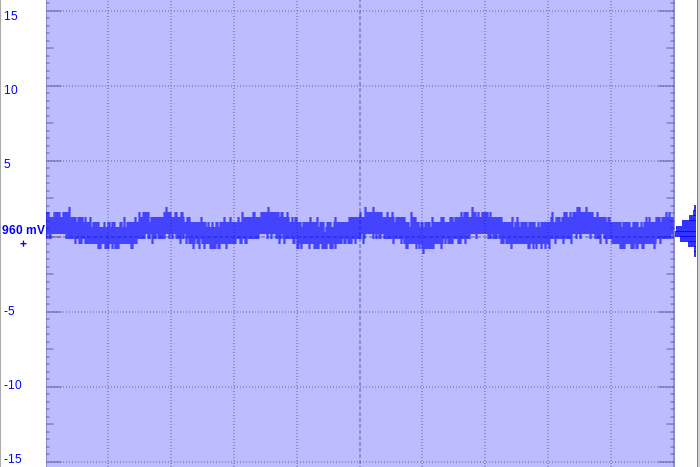
Output signal noise analysis. The input signal seems to perform well too, but the shaded blue region is much larger. This indicates the presence of some high-frequency noise -- later, I might try to eliminate this by implementing the additional low-pass filter that I left board footprints for. This noise measured to be 750 kHz or greater.
![]()
Input signal noise analysis. -
PCB Part 2: Analog input testing
09/03/2023 at 16:12 • 0 commentsThis log will give an in-depth report on the testing and ciruit alterations that were made to get the analog input signal circuit working as desired. The alterations were able to be kept to simple component swaps, so future boards can be ordered with just a few changes to the bill of materials.
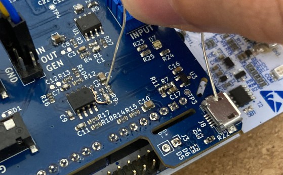
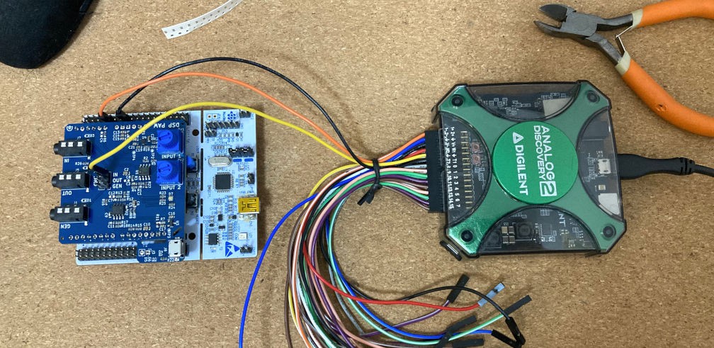
To analyze the signals, I hooked up my Analog Discovery 2 to the NUCLEO and add-on board. For the input signal path, the Discovery's waveform generator was connected to the add-on board's signal input and an oscilloscope probe was hooked to the ADC pin that receives the conditioned signal. A third wire gives us a common ground:
![]()
A couple of power supply observations
Once the add-on board was connected to the NUCLEO, some of the add-on board's power supplies were not behaving as expected. First, I noticed that the add-on board's +5V and -5V test pads were reading voltages around +/- 3.6V. The add-on board gives USB power to the NUCLEO through its VIN pin, and expects the NUCLEO to give that back on its 5V pin; however, revisiting the NULCEO's schematic proves that this is not the case.
![]()
The NUCLEO puts VIN through a 5V linear regulator and a protection diode before the "E5V" net, which is passed to +5V through a jumper. Both of these components create significant voltage drops for the power going through them:
![]()
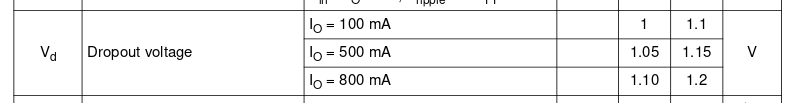
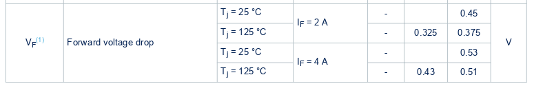
The LD1117S50TR experiences a "low" dropout voltage of around 1V. ![]()
The STPS2L30A diode drops voltage by 0.3 to 0.4V. Take the 5V input voltage and subtract the 1V and 0.4V drops and you get 3.6V -- just what we're measuring. Ideally, the add-on board would be re-routed to give its 5V USB power directly to the 5V pin, but for now we can get by since the operational amplifiers (the only components using +/- 5V) just need +/- 2V to properly handle our signals.
Analog voltage reference
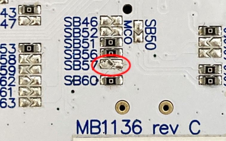
I also verified that 2.048V analog voltage reference now that the NUCLEO board was connected, and measured... 3.3V. That would be the NUCLEO's default reference voltage, with the schematic showing that a jumper handles this connection. We'll need to desolder a jumper on the bottom of the NUCLEO board.
![]()
SB57 connects 3.3V to the microcontroller's voltage reference pin. This might present an issue going forward, since it means users will need to be comfortable with (and have the means for) desoldering this jumper. The 2.048V reference is far less noisy than the NUCLEO's 3.3V, so this decision will have to take some thought.
Apart from this connection, the resistor divider on this reference that's used for shifting the input signal above negative voltage is incorrect. The division needs to be by four, not two as the board was accidentally designed for. I should have caught this before ordering the boards by comparing schematics with the previous iteration, but oh well... the fix is an easy resistor swap on R7 (from 10k to 30k):
![]()
Some of these resistor pads are thin and flimsy, so some extra solder is needed to make the connection sturdy. Input signal analysis
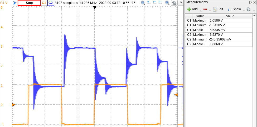
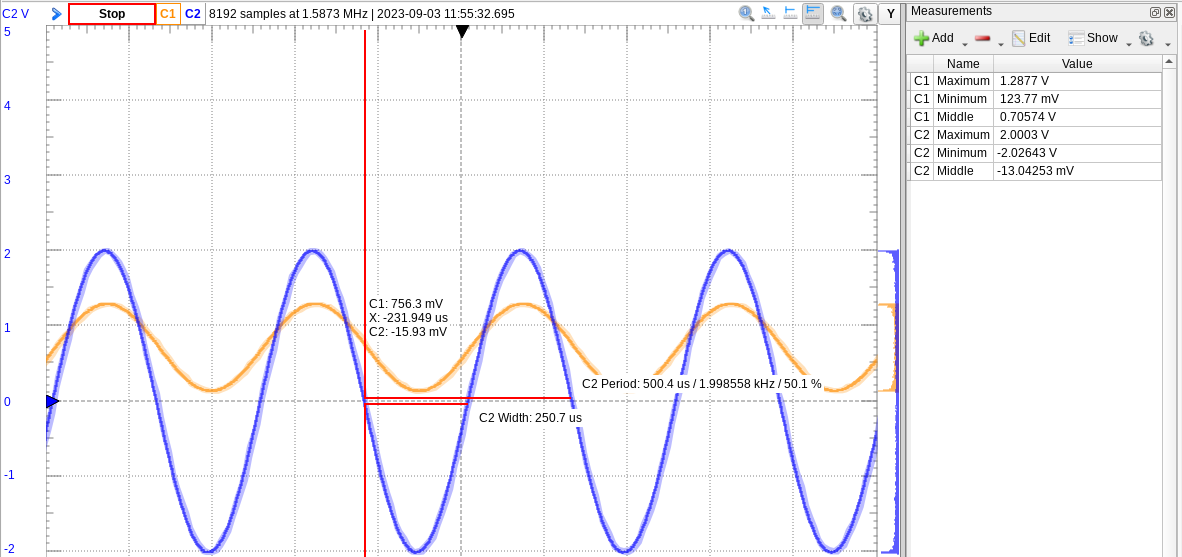
With the above out of the way, it's time to turn the oscilloscope on and run some simple tests. We start with a 0V signal to check noise and offset (+/- 2V is converted to 0 to 2V, so a 0V input should read on the ADC pin as 1V):
![]()
Sadly, this is not a clean signal or a 1V signal. A closer capture shows that we're getting a sine wave with a 1.4V swing at 1.4 MHz.
![]()
This is a clear indicator that one (or both) of the opamp stages are unstable and creating oscillations with their feedback networks. The remedy is often found with capacitive adjustments: we can either balance the input and output capacitance, or we can add capacitance to the feedback network to create a delay that stabilizes the feedback. I tried adding output capacitance first, and while that cleared the oscillation it also created a low-pass filter that ruined signal inputs above 1 kHz. Adjusting the capacitance to allow higher frequencies would lead the opamp back into instability.
![]()
The above should have been a smooth, 1 kHz sine wave. So, we go with the feedback capacitor. A capture of the first stage opamp's output showed a stable signal, indicating that it was the second stage creating the oscillation. This means that capacitor would stack onto R2, and after some trial-and-error (touching through-hole ceramic caps to R2 while monitoring the output) a value of 100pF was chosen. The clean output can be seen in the following scope captures.
![]()
R2 (top center) with a 100pF capacitor stacked on top. Gain and offset adjustments
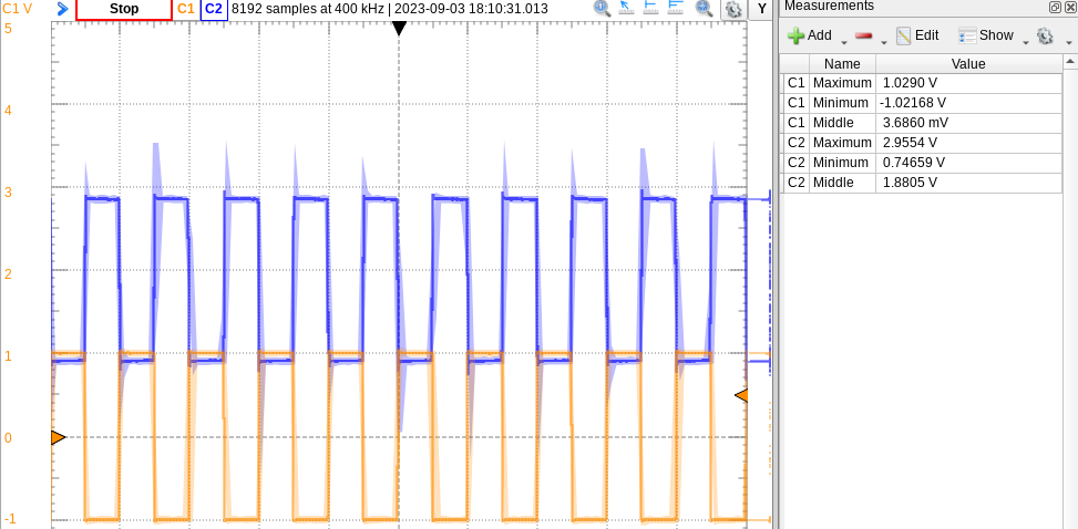
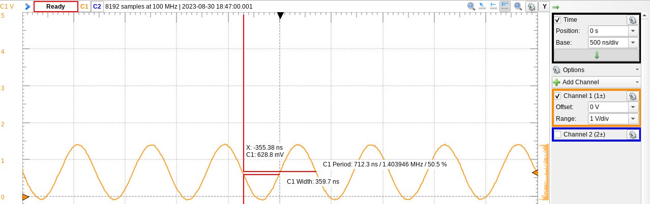
With the opamp filter stabilized, we can now compare the overall circuit's output against an input sine wave. I set the input amplitude to 2V so that we can check the full range of supported voltage.
![]()
Blue: Signal into add-on board INPUT. Orange: Signal seen on ADC pin. There are two problems to tackle here: first, the output onto the ADC pin is not swinging from 0V to 2V as was expected; second, that output is only at an offset of 0.7V when 1V was expected. I went after the incorrect gain first, since there's a chance that it is also affecting the added offset.
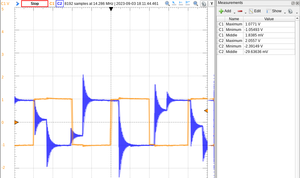
The input signal's gain is adjusted by the second filter stage which is a basic inverting amplifier with G=0.5. In the above capture, we're only seeing a measured gain of 0.29. While the inverting configuration does allow for gains less than one (G = -Rin / Rfb), some extra research has shown that gains less than unity (i.e. 1.0) are likely to go unstable, possibly causing this problem. A separate thought of mine wonders if the first filter stage is influencing the gain: if we consider the first stage's feedback resistor of 9.09k as additional input resistance, the gain of the second stage theoretically becomes 0.34 -- much closer to 0.29.
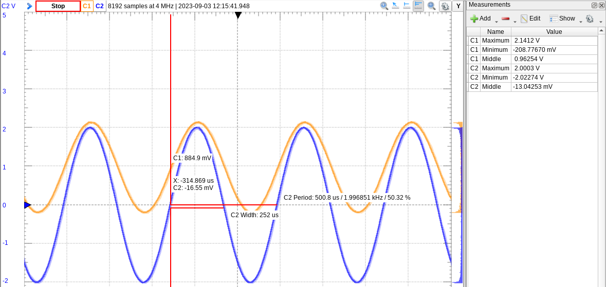
To test both possibilities, I swapped the second stage's input resistor to 10kOhms. This either creates stable, unity gain, or a theoretical gain of 0.52.
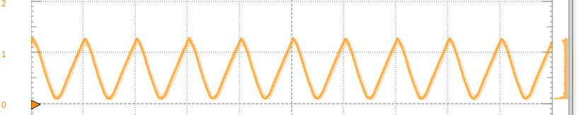
![]()
Blue: Input signal. Orange: Output to ADC. The measured gain has increased to 0.58, suggesting that input resistance from the first stage is most likely factoring in. We now get a swing slightly beyond 0 to 2V, and the offset has also increased for the better to 0.963V.
For the signal offset, I inspected the circuit's initial series capacitor next. It's meant to cancel DC offsets in the input signal, and does a good job at that, but it hat also turned out to introduce a constant offset itself. Before this capacitor, the input signal has a "middle" of -13mV; after the capacitor, this drops to -64mV. That drop remains constant when the input signal's offset is adjusted.
The difference in drop is 50mV, which is very close to the difference between our current output offset of 0.963V and the ideal 1.0V. After removing the capacitor and shorting its pads, we achieve an output offset of 0.997V:
![]()
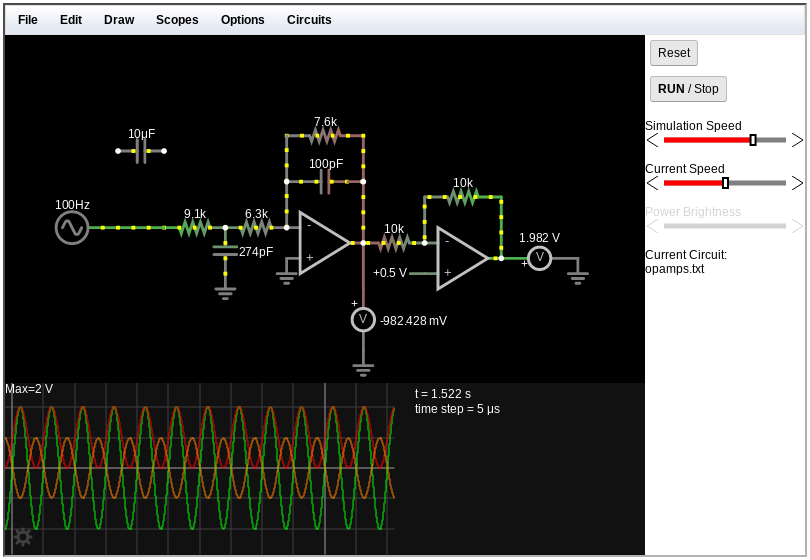
Blue: Input signal. Orange: Output to ADC. The span of the ADC signal has also closed in on the 0 to 2V range, though we're still seeing peaks with negative voltage. There's a risk that this will damage the ADC over continuous use, so a slight reduction in gain would be beneficial. At this point, I turned to the Falstad Circuit Simulator to simulate the two opamp stages. This would both confirm that both the current design is sound, and allow me to determine the final change(s) to perfect the output.
![]()
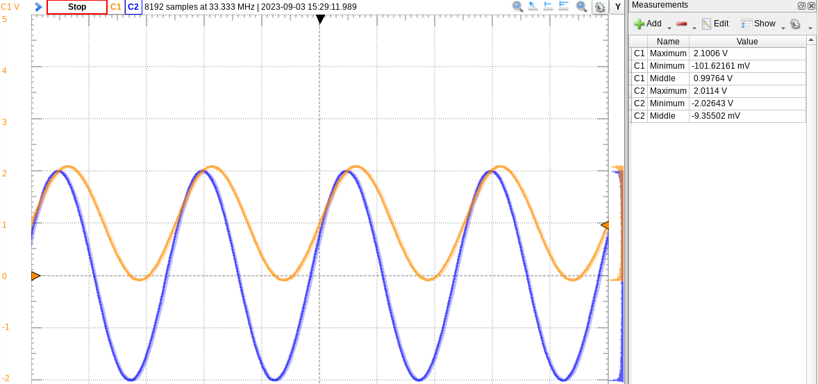
With some trial-and-error, I found that slightly decreasing the first stage's feedback resistor would produce an ideal gain factor. I have 7.5kOhm resistors handy, so I swapped one into the circuit and checked the result:
![]()
Blue: Input signal. Orange: Output to ADC. Finally, we reach acceptable performance. The gain could still be improved by ordering a different feedback resistor to bump the gain up a little more.
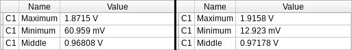
Towards the end of testing, I noticed that our measured results may not be as far off as we have observed. The two tables below show measurements of the ADC waveform with (left) and without (right) the second probe on the blue input signal -- improvement is seen in every measure. Even better, the below numbers are from a test with the DC-blocking capacitor added back in, so that's one less change needed for future boards.
![]()
Left: With second probe connected. Right: Without second probe. Frequency analysis
For a final test, let's confirm that the input signal path can accommodate the entire frequency range that we wish to sample. Our upper bound is specified to be 48 kHz, since our highest sampling rate is 96 kHz. The lower bound is no more than 20 Hz to allow all human-hearable frequencies; going lower is welcome, but issues may arise from circuit capacitance and DC blocking.
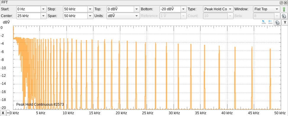
I used a Fourier transform to capture the strength of the input signal as I swept it from 48 kHz down to 10 Hz. The peaks throughout the graph are the frequencies that I tested:
![]()
The signal proves to be strong across the spectrum, just barely dropping by -3dB at 50 kHz. This performance is just right for our needs.
Conclusion
The input signal path has been tested and adjusted to reach the range of performance this project needs. The next step will be to validate the output signal path, which I'm going to separate into another project log since this one has become so long.
Once the output is tested, we'll get to run some algorithms through the new board capture the results. I'll most likely do this in a video to have a true "demo" of the project.
As a final note, here is a picture and summary of the changes made to the board so far:
![]()
- R7: Change to 30 kOhm for correct voltage reference division.
- R1: Change to 7.5 kOhm to reduce gain of first opamp stage.
- C2: No change. Was initially removed to improve final signal offset, but adding this back in at the end saw no performance loss.
- R5: Change to 10 kOhm to increase gain of second opamp stage.
- R2: Stacked 100 pF capacitor on top of the resistor to stabilize the second opamp stage.
-
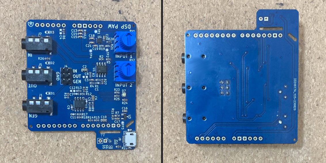
PCB Part 1: Arrival and voltage testing
09/01/2023 at 17:53 • 0 commentsThe assembled PCBs have finally arrived, and after some testing and tweaking have proven to be good successors to the previous design. There is a ton to go over for the bring-up process; I'll share some initial observations and testing here, and then in the following log take a deep dive into validating the input and output signal paths.
Although the 3D renders were of green PCBs, I chose to stick to the blue color that the previous iteration used. It compliments the NUCLEO deveopment board better.
![]()
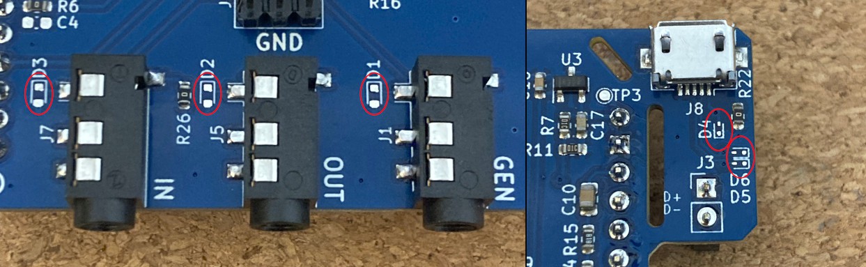
The USB breakaway came out better than I expected, and feels sturdy when a cable is attached. There's only one issue with the board that's immediately noticable: the protection diodes are missing.
![]()
I went back to my order confirmation, and oddly enough the BOM used for assembly did not include any diode part numbers. I double-check the original BOM next to ensure my sanity, and...
Reference Part Number D1,D2,D3 ESD5Z2.5T1G D4,D5,D6 DF2B7AFS,L3M ...we realize that the BOM exports as a comma-separated file (.csv). The comma in D4-D6's part number probably caused an error and made the ordering page drop that row. I guess that a similar issue exists for the part number with a period in it. Fortunately, these parts are not essential to the design, though it's a shame that this wasn't caught.
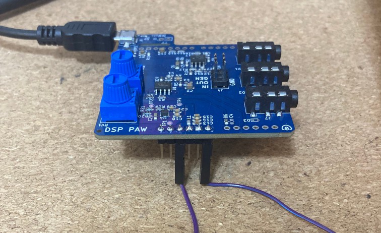
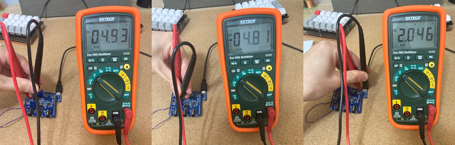
Anyways, we now move on to powering the board up and making sure the power regulation is correct and stable. It's best to test this before risking the connection to the microcontroller board, so I soldered on a little header for the power pins and plugged in the USB cable:
![]()
Nothing put out heat or smoke, which is good. I used a multimeter to check the power supply test points: ground, +5V, -5V, and the 2.048V voltage reference -- everything looks good!
![]()
The USB cable does not supply a perfect +5V, but that doesn't really matter. The opamps only need +/- 2V to properly handle the analog signals, so anything beyond that minimu should work well.
At this point, it should be safe to fully connect the new add-on board to the NUCLEO and test the inputs and outputs completely. All that is needed is a pair of 14-pin male headers (to break apart and fill the Arduino connector), and a 2-pin female header to connect to the microcontroller's USB data pins.
![]()
By sticking the headers into the NUCLEO board, I could solder them onto the add-on board with everything lined up and fitting:
![]()
Before and after. I'm proud of the solder joints -- it takes practice to make them "clean". The input and output circuits are certainly more complex than the power supplies, and that'll show in the amount of testing and adjusting they needed. Stay tuned...
-
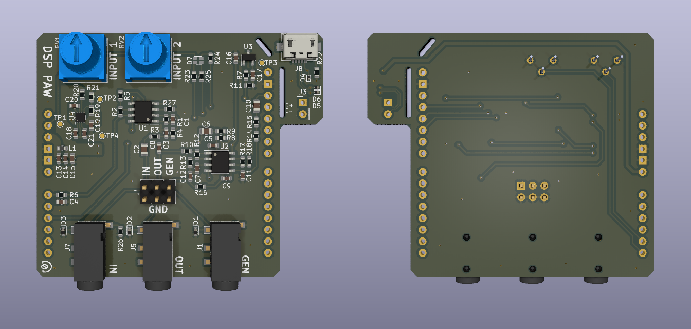
PCB layout and Arduino footprint
08/19/2023 at 12:26 • 0 commentsLayout of the new add-on board is complete. I should note that the schematic and board layout are being done with the open-source electronics design suite KiCad. This is my first "real" design using KiCad, and the process has gone a lot smoother than I anticipated. There is a large community available for support, plenty of component libraries available, and even some one-click gerber generation plugins for PCB prototype manufacturers for easy order quoting. It's my personal recommendation to learn KiCad if you are in need of circuit design software.
Change to Arduino footprint
A significant design change was made during the process of layout which is important to cover first: the board is now based on the common Arduino header format rather than the “ST Morpho” format used by STM NUCLEO development boards. This change greatly expands the compatibility of this board with other microcontroller development boards with no practical compromise. The layout process revealed that nearly all connections are either routed through or could be substituted with pins on the Arduino header of the NUCLEO board.
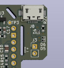
The exception is the pair of USB data pins. Since these are near a corner of the board, the USB circuitry was moved to be contained in that corner. Since this is a NUCLEO-specific requirement, cut-outs were made to allow removing this portion of the board for development boards that do not require it:
![]()
Layout process and results
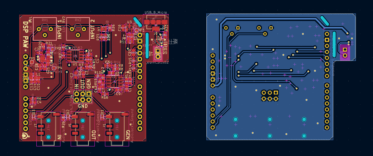
The layout could have been done with either two or four copper layers. The four-layer option would allow for two internal copper layers, where typically one carries a ground plane and the other carries DC power traces. Isolation of power traces and insulation of signal traces through the ground plane would minimize the possibly of induced signal noise, although with the drawback of increased manufacturing cost. Additionally, that level of care for signal quality is not quite necessary for the intended applications of this board. Since board design was achievable with two layers, the two-layer approach was taken.
All components were kept on the top layer of the board. Available board space allowed for this, but it also simplifies board manufacturing. Prototype PCB assembly services typically only offer component placement on one side of the board; in this case, that means only the Arduino and USB pin headers need to be soldered by hand after delivery.
![]()
Both layers were filled with ground pours (i.e. spreads of grounded copper) to surround the traces and minimize the potential transfer of noise between them. Other common techniques were employed in the design: components like decoupling capacitors were kept near their sources, application notes were followed for the four ICs circuits and layout, and some consistency was made on trace directionality (top layer prefers north-south paths, bottom layer prefers east-west). Power circuits were kept away from the analog circuit paths where possible. Ground vias were spread throughout the board to ensure consistent grounding. And finally, KiCad’s electrical and design rule checks were used to confirm a sound design.
A nice 3D rendering
KiCad also features the ability to create 3D models of circuit board designs, and so I’ve done that for the add-on board:
![]()
The board is 63mm at its widest, and 53.5mm in length. The previous NUCLEO-based design was 70x55mm; fortunately, the reduction in board size was manageable.
Design files are open source
The new add-on board design is released under the CERN Open Hardware Licence Version 2 - Strongly Reciprocal license, a license made specifically for open hardware. I am also working on a new source repository for DSP PAW which contains all of the project's firmware, software, and hardware files. It is hosted on both my personal server and on GitHub. The KiCad project files can be found here. PDF versions of the schematic and fabrication drawing will be made available by the time the prototype batch of these boards is ordered.
-
Schematic design changes
08/18/2023 at 01:02 • 0 commentsThe add-on board’s revised schematic and board layout are practically complete; the next couple of logs will go over the significant changes in the hardware design for this next iteration.
The primary changes in the schematic come down to the filtering and conditioning of the input and output signals given the new signal specifications. Design tips and strategies were taken from multiple resources to maximize accuracy and minimize noise. This highlights the best piece of advice I can give to those designing circuits and schematics: use all of the resources at your disposal. Nearly all datasheets for integrated circuits (ICs) include detailed “Application” sections that show circuits, discuss component selection, provide calculations to meet design parameters, etc. Following these instructions will ensure a sound design. Major manufacturers also have vast collections of application notes that cover a wide array of electronics design topics. These can be found on their websites, or simply by searching the internet. There’s no reason not to work off of proven designs and knowledge when you can.
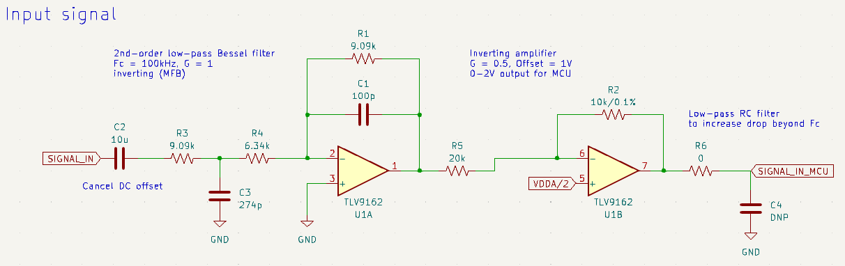
Input signal
Previous designs of the add-on board used basic inverting amplifier configurations to achieve the simple goal of scaling signals to the desired voltage ranges. Amplifier ICs were chosen solely on the basis of if they can achieve this goal. Later on, slight changes with passive components were made to reduce high-frequency noise.
For the next design, I turned to an application note from Texas Instruments (TI) on “Active Low-Pass Filter Design” and the accompanying Filter Design Tool. Given the project’s new specification on maximum sampling rate, a second-order active filter could be used to achieve an optimal signal-to-noise ratio. The max rate of 96 kHz was rounded up to 100 kHz for simplicity.
![]()
A Bessel filter was chosen to avoid gain overshoot below the cut-off frequency, at the cost of reduced attenuation performance. To compensate, the Multiple Feedback (MFB) architecture was used to optimize the high-frequency response; placeholders for an additional low-pass filter stage (R6 and C4 in the above photo) were also added in case increased attenuation is necessary. MFB also has reduced sensitivity to component variation, allowing for some component cost savings.
The Bessel filter is preceded by a series capacitor that cancels out any DC offset in the incoming signal. The previous design instead canceled the offset by feeding the ground of the input audio jack into the differential amplifier; however, this approach was not proven to be sound or “correct”. A series capacitor is an easier and safer choice. The value of 10uF is fairly arbitrary, and will be adjusted during testing if needed.
The second stage of the input signal path is a simple inverting amplifier, as the MFB architecture of the first stage is also inverting. The second stage is also used to add a DC offset to the signal, bringing it into the acceptable voltage range for the ADC.
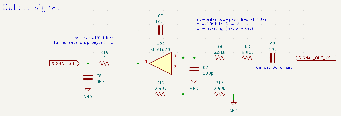
Output signals
The output signal (and signal generator output) uses a Bessel filter just like the input signal. A Sallen-Key architecture is chosen this time though, primarily for the fact that it produces a non-inverting configuration. This means there only needs to be one active stage in the output path. The drawback is a potential reduction in high-frequency response; the optional low-pass RC filter is included in case this reduction is worse than desired.
![]()
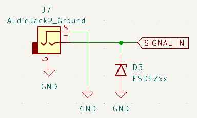
ESD protection
This design introduces ESD (electro-static discharge) diodes on the audio jacks and USB port. ESD can occur on any component that interacts with the outside world (e.g. human touch), so it is good practice to include this kind of protection. In a worst-case scenario, unprotected ESD could damage components on either of the add-on or microcontroller boards.
The choice of diode is flexible as long as the diode does not breakdown within the normal voltage range of the line that it is connected to.
![]()
Source supply filtering
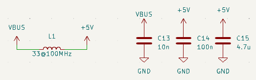
Finally, some passive filtration was added to the source power supply (5V from the USB port) to prevent it from being a possible noise source. The inductor and capacitors work to create a low-pass filter, with the variety of capacitors combating different frequency ranges. The chosen component values are based on existing designs (and following advice from this blog post) and are open to adjustment during testing.
![]()
-
Design decisions and specifications
08/08/2023 at 23:33 • 0 commentsThis project has compiled a set of specifications over its lifetime which influence the design of its hardware (i.e. the add-on board) and the capabilities of the device and its software overall. The buildup of these "specs" happened fairly naturally, or arbitrarily; however, these need to be fine-tuned for the upcoming hardware iteration since it aims to be a more-or-less "finished" design. As a result, a few of these specifications have changed. I'll take this chance to list out all of the current design specifications, as well as discuss some of the decisions that led up to them.
I'm sharing these now since the schematic for the next add-on board is nearly complete. These are the specifications it follows, and the next project log will show how the implemented circuits meet these requirements.
Sampling rate and buffer size
These two values determine the speed and quantity of incoming data that needs to be processed. Limits for these values depend on the given application; for DSP PAW, educational and audio applications are the primary target.
Educational projects will generally lean towards simplicity, so we would like to avoid super-fast sampling rates and huge sample buffer sizes. On the other end, too low of a sampling rate would cause slow algorithm reactions and make testing a nuisance.
For the lower bound, a fairly arbitrary choice of 8 kHz was made. This allows for working with slower signals as well as some audio since the frequency is a telephony standard. This rate is also easy to create with microcontroller (MCU) clock -- the MCU needs an 8 kHz clock to sample signals at 8 kHz.
The upper bound sampling rate was inspired by audio applications. The two most common audio recording rates are 44.1 kHz and 48 kHz. Generating a 44.1 kHz clock proved to be difficult, especially since the one clock would also have to support the lower frequencies (e.g. 8 kHz). So, design leaned towards 48 kHz, ultimately choosing its double (96 kHz) as the maximum. This gives a maximum Nyquist frequency of 48 kHz, meaning signals up to 48 kHz can be sampled without aliasing/distortion.
The STM32L476 microcontroller can actually support sampling at up to 5 MHz, but for audio and education there is little need to go faster than the chosen limit. Getting anywhere close to the MHz range would both reduce the algorithm execution window to an unusable size, and interfere with the microcontroller’s essential USB communications with the computer.
For buffer size, the configurable range was made to be between 100 and 4,096 samples. The upper limit was partially a result of the microcontroller's constrained memory, though this allows for up to half a second of signal data when sampling at 8 kHz. Smaller buffer sizes are handy for simple algorithms and/or faster algorithm reaction times.
Signal amplitude
The other primary factor of a signal apart from its frequency is its amplitude. Supporting larger amplitudes means flexibility with external signals, though it also requires caution regarding electrical safety of the hardware. The MCU can only handle voltages between 0V and the ADC reference voltage (3.3V by default), so the add-on board needs to scale signals to or from that range.
Previously, an arbitrary decision to support +/- 3.3V was made. This range is wide, and allowed us to rely on the MCU’s default ADC reference. The next design iteration will see a reduction to +/- 2V, for a few reasons: first, this means the addition of an external ADC reference which will eliminate power supply noise from affecting the signals; second, the MCU's use of the 2V reference will lead to better accuracy and precision...
Third, the project's target applications do not need the additional range that was previously allowed. Educational applications will either use the on-board signal generator, which follows the chosen limit, or external hardware which can most often be configured to an acceptable amplitude. For audio, line levels should practically always be within +/- 2V. For the rare case that incoming signals exceed this specification, protection diodes are being added to the add-on board.
Other specifications
The other features of the add-on board are more or less "set in stone," as they have not changed since the initial prototype:
- One signal input port and one signal output port: supporting multiple DSP streams at once would be a daunting task.
- One signal generator output: there is little if any need for multiple generator outputs.
- Two "parameter" potentiometers: more may be added if enough applications warrant it; a software interface for this feature could also be made.
- 0.1"-pitch headers and 3.5mm jacks for the signal I/O: these seem to be the most common and easy-to-use connectors.
- MCU interface through the "ST Morpho" headers: chosen since the project is meant for NUCLEO development boards, though this could change or expand if other boards are to be supported.