ROFLhoff
-
Analog Meters
07/10/2023 at 22:55 • 0 commentsIn this update I will talk about how I added analog gauges into my project to easily display the charging progress of connected batteries.
I did not originally have analog gauges for this project. I had a couple 16x2 LCD displays but I was firm on not incorporating a microcontroller into this project. So I went and looked on amazon for gauges. I wasn't sure what I was going to find. Most gauges were listed as measuring very small amounts of current (tens to hundreds of microamps), and it turns out this is the most common and versatile kind.
These gauges use a "D’Arsonval" movement, which operate using small currents and also have enough delay in movement that there is signal averaging builtin, for free.
I picked two gauges that were labeled 500uA full scale, and the scales were labeled to be used to directly measure that current. My plan is to make new plates to show proper scales.
Both gauges will be measuring voltages in circuit, and not currents, so the gauges must be configured. This is done through a series resistance between the measured voltage and the gauge. To calculate what resistance is needed, we can use the following equation:
![]()
where V_fs is the maximum voltage to measure, i_fs is the given full scale current, and R_internal is a property of the specific gauge. This value is pretty small compared to R_series so it can be omitted with the understanding that the gauge will swing close to, but not to its maximum.
The meter that is measuring current will see at most 5V, we find that the series resistance is a simple 10K ohms (ignoring R_internal).
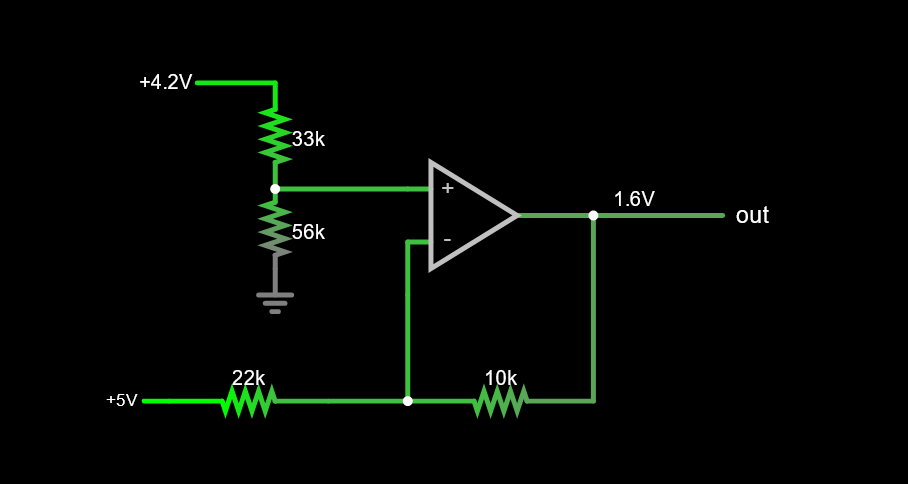
The other gauge that is going to measure the battery voltage will be slightly trickier to setup. If the gauge is connected the same way as the current gauge, and if the practical range seen will be from 3V to 4.3V, this is going to be a rather narrow section of the gauge. It would be nice to utilize more real estate to make the battery voltage easier to read at a glance.Signal Conditioning is another good use of Op Amps. We can take the battery voltage and do both offsetting and scaling so that we get the most of the usable deflection range. The following diagram is the Op Amp configured to both offsetting and scaling using common resistor values.
This particular Op Amp configuration is mentioned in a fantastic Texas Instrument document called "Op Amps for Everybody" in section 4.2, Figure 4-8. The following section goes over the equations to convert offset/scaling to resistor ratios. Do keep in mind that the LM358 is not a rail-to-rail Op Amp, and the output cannot reach the positive supply voltage.
In my situation, I wanted to take an input voltages of 2.5-4.6V and have the Op Amp output ideally 0-500uA. In our case we can get away with generating an output voltage and passing that to a gauge with a series resistance to properly set the full scale reading. We can implement an acceptable design with E12 value resistors. The input of the amplifier is best connected to the V_sns signal.
![]()
Not shown is a 3k9 resistor from the amplifier output to the 500uA meter for the voltage gauge. This lets the roughly 1.85V output of the amplifier result in full scale movement on the gauge.
What comes next is creating a custom scale for the gauge instead of seeing "0-500uA" as the output.
Looking online, I found resource from element14, where a user named shabaz created a python script that make a custom scale. It's the file named "app.py" in this project. I had tweaked it to make markings in roughly 100mV steps from 3.0V all the way to 4.6V, with thicker markings for important levels like 3.0V, 3.6V(safe LFP voltage), and 4.2V(safe Li-po voltage).
The problem is that these markings had to line up with the full scale of the gauge. My calibration procedure was to:1. Connect a variable voltage source to the input of the Op Amp Circuit, and an ammeter to the output of the circuit.
2. Set the input to 2.9V and increasing in 100mV steps, measure the output current.
3. In the code, set each mark to the measured current.
4. Run the code, a svg file should be created.
5. Open the svg file in an editor and add text as desired.
6. Print the finished scale, and affix it to the gauge.My calibration table looked like this:
4.6v = 488uA
4.5v = 469uA
4.4v = 448uA
4.35v= 434uA
4.3v = 425uA
4.2v = 402uA
4.1v = 378uA
4.0v = 357uA
3.9v = 333uA
3.8v = 312uA
3.7v = 285uA
3.6v = 262uA
3.5v = 240uA
3.4v = 220uA
3.3v = 190uA
3.2v = 168uA
3.1v = 149uA
3.0v = 124uA
2.9v = 100uAThis Op Amp circuit works fairly well, the usable voltage range had expanded and centered on the gauge.
In the centerpiece image for this project, both analog gauges are displayed in action. The green battery is in the constant current stage of charging, and the CC mode LED was on to confirm it. There was 1 Amp going into the battery, and the current battery voltage was nearly 4.0V. A nice unintended effect with the amplifier was that when the battery was removed, the needle on the gauge hovered in the zone before the 2.9V tick. This is a handy way to note that the device was on and no battery was attached. When the device was turned off and had no battery connected, the needle was all the way to the left.
In the next post, the gauge circuitry will be modified so that a button can toggle the gauges to show either the Current/Voltage setpoints, and the Battery Current/Voltage levels.
-
The 4-ish Stages of a CCCV Charger
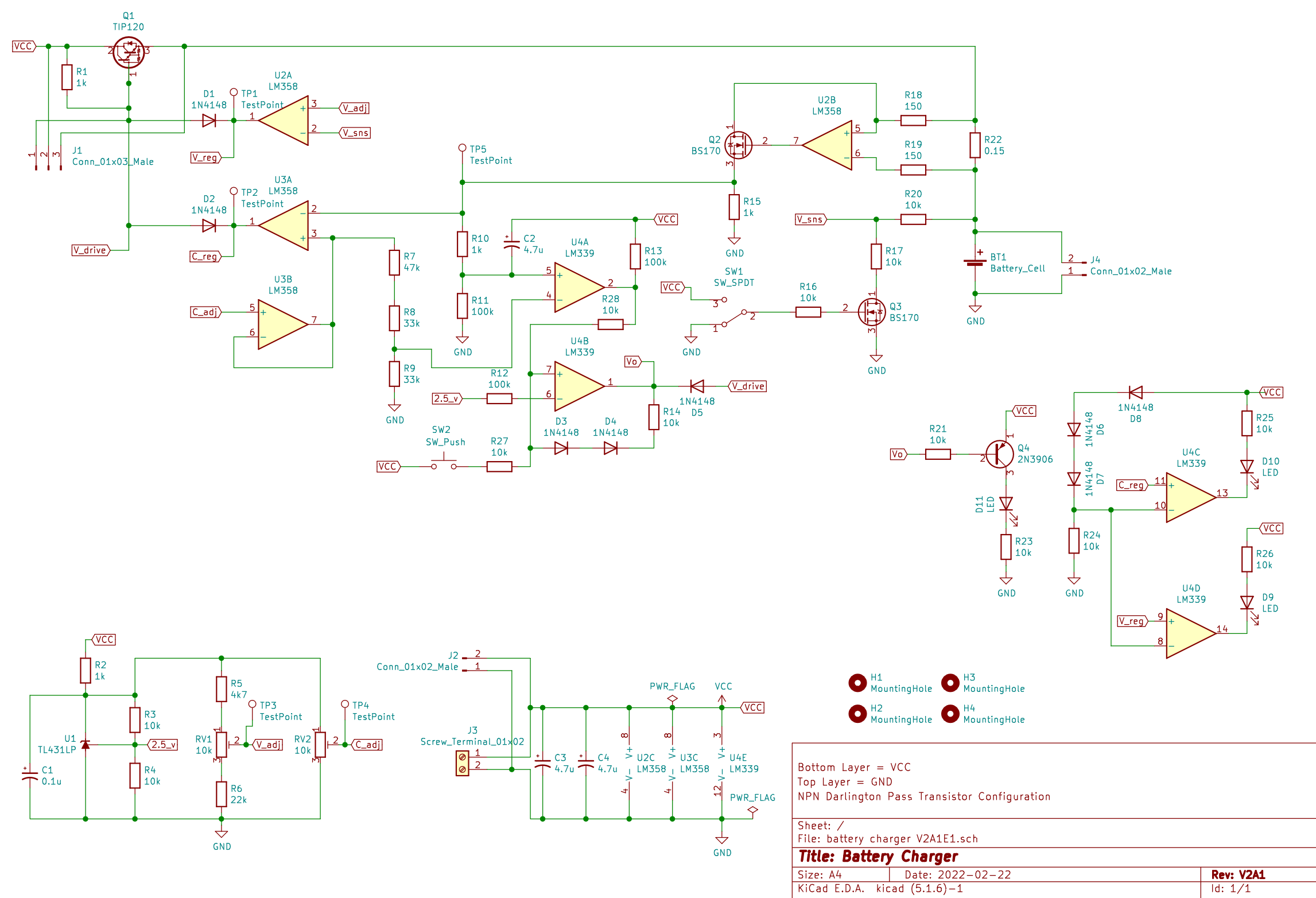
06/22/2023 at 05:09 • 0 comments![]()
The posted schematic is the version I created a PCB design with, and sent to a fab company to produce samples of. Part designations will be referenced to this schematic unless a new design succeeds this version.
The basic principle of this design is a combination of 4 parts:
- Pass Transistor(s)
- Constant Current (CC) Amplifier
- Constant Voltage (CV) Amplifier
- Shutoff Latch/Comparator
And auxiliary components like voltage references, switches, fans and heatsinks.
1. The Pass Transistor(s)
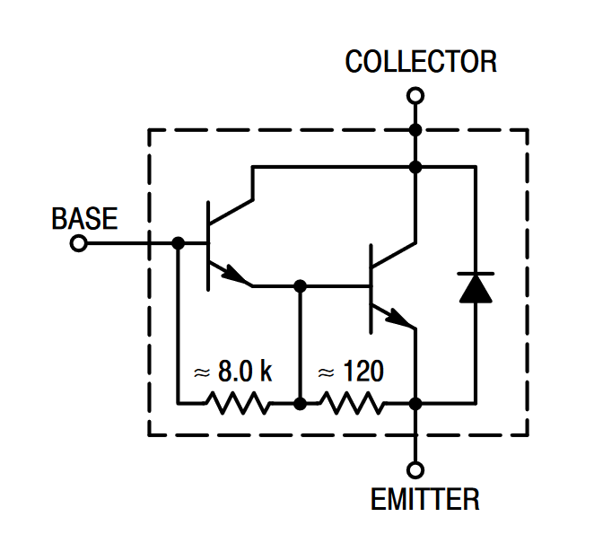
To keep with the theme of creating a working design with simple and widely available components, this design will start with an NPN BJT Darlington Pair. This will create a couple limitations in the design. First off, the TIP series of Darlington Pairs have extra resistors and a diode built-in that simplify using the device as a switch. The following image shows the internal construction:
![]()
The problem lies in the diode. If a battery is connected to the charger and the power is disconnected, the Op Amps and TL431 regulator will now be back-powered from the connected battery. This has the potential to drain the battery. A quick fix is to simply add a forward-biased diode between the Darlington Pair and the current sense resistor R22. This diode leads me to bring up another point.
To drive this Darlington Pair in the active region, the base pin will sometimes need to be driven to voltages that the LM358 output stage can barely reach. To properly estimate the needed base voltage, we need to get the worst case condition. This occurs at the switch between the CC and CV stage in charging. The battery is at its highest voltage, and the voltage developed across R22 is greatest. To put into equation form, this appears as:
![]()
When I had configured my charger (supplied with 12.2V) to charge an 8.4V 2S lipo battery at 2 Amps, I noticed that the charger could not sustain 2A when the battery voltage got higher than roughly 8.2V. I figured that the base pin was not being driven hard enough, so I had temporarily replaced the base drive resistor R1 with a lower value.
Looking at the TI datasheet for the LM358, it is stated that the output can't get any closer than about 1.5V from the positive rail. Given that in the current design, there is an additional forward-biased diode that controls the base pin, this lets the Op Amp output control a slightly higher voltage of 0.8V away from the positive supply.
We can bandaid fix this problem by running the charger at a higher voltage, but since this is a linear charger, this is a waste of power and users would need a bigger heatsink to compensate. Not a real solution. The proper fix is to design the base pin to be controller with lower voltages. A PNP darlington pair or P-channel MOSFET would make better pass transistors.
Be sure to connect a heatsink and fan to whatever pass transistor you use. The peak power that is wasted is:
![]()
When charging a 1S lipo battery at 2A, the pass transistor was producing over 16W of heat at peak. I used a heatsink originally used to cool an old Celeron 366MHz CPU, it came with a fan plus mounting bracket for active cooling, and it handled the load with no issues. I could touch the heatsink and not burn my fingers.
2. Constant Current Amplifier
Op Amps U2B, U3A, and U3B form the CC amps.
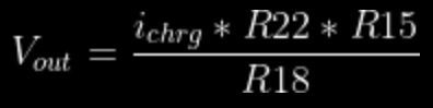
U2B is converting the voltage across the current sense resistor R22 and generating a single-ended output signal on R15. The output equation for this amplifier is:
![]()
In my design R15, R18, and R22 are selected such that 1A going through R22 generates 1V across R15. This allows an intuitive link between the measured current and the current set point. The voltage that is generated through the potentiometer RV2 is buffered through U3B. Since RV2 is connected straight across a 5V reference, this potentiometer will allow the user to adjust the charger to send up to 5A into the battery. This is a rather high amount of current compared to the cheap commercial offerings, but some component substitutions will have to be made. The current sense resistor will have to be rated for high currents (with additional adjustments to R15/R18), beefier pass transistor and heatsink will be needed.
R19 is selected to be the same value as R18 to compensate for the input bias currents of U2B. Q2 is preferred to be MOSFET rather than a BJT. if a BJT is used for Q2, there will be a small amount of current going into the base and out the emitter, this will introduce an error in measured current. This error is approx:
![]()
U3B is simply a voltage buffer for RV2. This eliminates the loading that resistors R7-9 would create in combination with the paralleled lower "leg" resistance of RV2. The output of U3B is fed into the non-inverting input of U3A to form a reference for negative feedback regulation.U3A is the heart of the constant current regulator. It is connected to form negative feedback. The output is connected to the pass transistor's base pin with a reverse-biased diode, D2. When the battery voltage is below the CV set point, the CC Op Amp output is actively regulating the pass transistor to maintain a constant current. When the battery voltage rises to the CV set point, the CC Op Amp goes high (reverse biasing D2), which would let our metaphorical brick run the car wild if not for the CV Op Amp now regulating.
3. Constant Voltage Amplifier
Op Amp U2A forms the CV amp.
Just like with U3A, we have negative feedback to control the constant voltage regulator. The potentiometer RV1 is our method of controlling the CV set point. There are two extra resistors R5 and R6 ,which together with a reference voltage of 5V, restrict users to a set point range between 3.00V and 4.36V. These are values for people using LFP or LCO/LMO/NCA/NMC-type chemistries. Lithium Titanate chemistry batteries have a much lower CV set point, so if this charger is going to be used for these, please adjust these resistors for such an application.
The measured voltage is connected through resistor R20 to the inverting input of U2A. This resistor normally has no effect on the circuit when the switch SW1 is in the "1S" position. When SW1 is in the "2S" position, there is another 10k resistor, R17, that is connected to form a resistive divider with R20. A low resistance MOSFET should be used to minimize voltage error. This basically halves the input voltage to U2A, so that a 2S battery can be treated like a 1S battery. Please note that this charger does no attempt at cell balancing. If you need to balance a multi-celled battery and have to use this charger, expose the individual leads to each cell and charge them one at a time.
The output of U2A operates the same way as U3A. When the output falls out of regulation, the output is driven high, and the diode D1 is reverse biased.
4. Shutoff Latch/Comparator
Comparators U4A and U4B create a latch to turn off the charger when the current into the battery drops to a low level. SW2 is a momentary push button that resets the latch to resume the charging cycle if the battery is discharged while connected, or if a different battery is connected to the charger while powered on.
Resistors R7-9 form the cutoff threshold for the latch. It's a resistive divider that is currently made to be a 0.33C threshold. I did this because I was impatient when testing. A better ratio would be 0.1C as that would maximize the amount of energy put in the battery. U4A is a comparator with the measured battery current and this cutoff threshold. When the battery is charging, the non-inverting input is higher than the inverting input, and the output is high. Once the current drops below the threshold, the output is low. This lowers the voltage on the non-inverting input of U4B, the latch.
When this latch is tripped, the output is held low, this effectively turns off the pass transistor and stops the charger. When SW2 is pushed, the non-inverting input is forced above the 2.5V level of the inverting input. This resets the latch and now the CC or CV amps can regulate again.
During testing on breadboard, the comparator U4A would trip during power on with a battery connected. I wanted this charger to "just work(tm)" in that scenario, so the components R10, R11, and C2 force the comparator in an untripped state during power on. R10 and R11 are in parallel with R15, so it's important to make R10 a low value and R11 a high value so the divider between 10/11 is as close to unity as possible. It would be best to select values so that:
![]()
and that R11 >> R10.
4-ish. Indicator LEDs
There are three LEDs in this design. D9 is the LED to indicate CV mode, D10 indicates CC mode, and D11 is the charge complete indicator.
Diodes D6-8 and R24 form a simple voltage reference. The outputs of the CC and CV amps are compared to this voltage. When each amp is in regulation the corresponding LED is on.
This part is a bit sensitive. Try to minimize the trace length of the outputs of U2A and U3A or the latch might trip unexpectedly.
Results
I am able to charge my batteries at 2A. There are several things which prevent me from trying out higher currents. I am using a 3W rated 150mohm current sense resistor which would likely fail in the 4-5A range. I also used some rather thin wires connecting the TIP120 to the main board.
I would recommend replacing R1 and R2 with better constant current sources. A jfet+resistor would work. I used a J113+470 ohm resistor to drive the TIP 120. This both reduced the idle current consumption of the circuit from 28mA down to 9mA.
My PCB files are included as a zip file in this project page.
Future improvements to the PCB would be to:
1. Redo TO-92 footprints for 0.1" spacing.
2. Adjust Capacitor footprint for same spacing.
3. Move Ext battery connector, expand footprint to mimic XT60 connector.
4. Include footprint to use jfet&resistor for pass transistor biasing.
5. +/- silkscreen labels for Fan/PowerInput/ExtBattery headers.
6. Move Test Points further away from potentiometers.
7. Make a Spacer for LED and resistor clearance from PCB.
8. Add Test Point for Battery Voltage (Rather than jabbing a spring contact on the batter holder)
My next update will detail the analog gauges I incorporated into the project.
Op Amp Based Lithium Charger
A linear CC-CV charger to handle various secondary lithium chemistries. Built with Op Amps and Comparators.