Close
0%
0%

10kW (30kW pulse) Electronic Load

All we need to do get some big resistors and connect them up in different combinations, right?

Similar projects worth following
For an upcoming project of mine, I'm going to need a big electronic load. REALLY big. I've foolishly decided to build my own.

Modern computer power supplies must handle transient current spikes far above their nominal rating (1800W spikes for 600W GPUs), and they should be tested under worst case conditions to ensure stability. However, commercial electronic loads are expensive, especially at high power levels.

Most electronic loads use a linear MOSFET-based design. However, none of the published designs reach the extreme sustained and pulse levels needed. This design uses an array of switched high-power chassis-mount resistors to produce any arbitrary load. This approach provides extreme scalability, low-cost, and high robustness. While simple in principle, the sheer scale and need for high frequency switching make this a challenging design.

Also suited for other applications, the sustained power capability makes this a good fit for 12V LiFePO4 battery testing.

Project Overview Video for Hackaday Prize 2023:

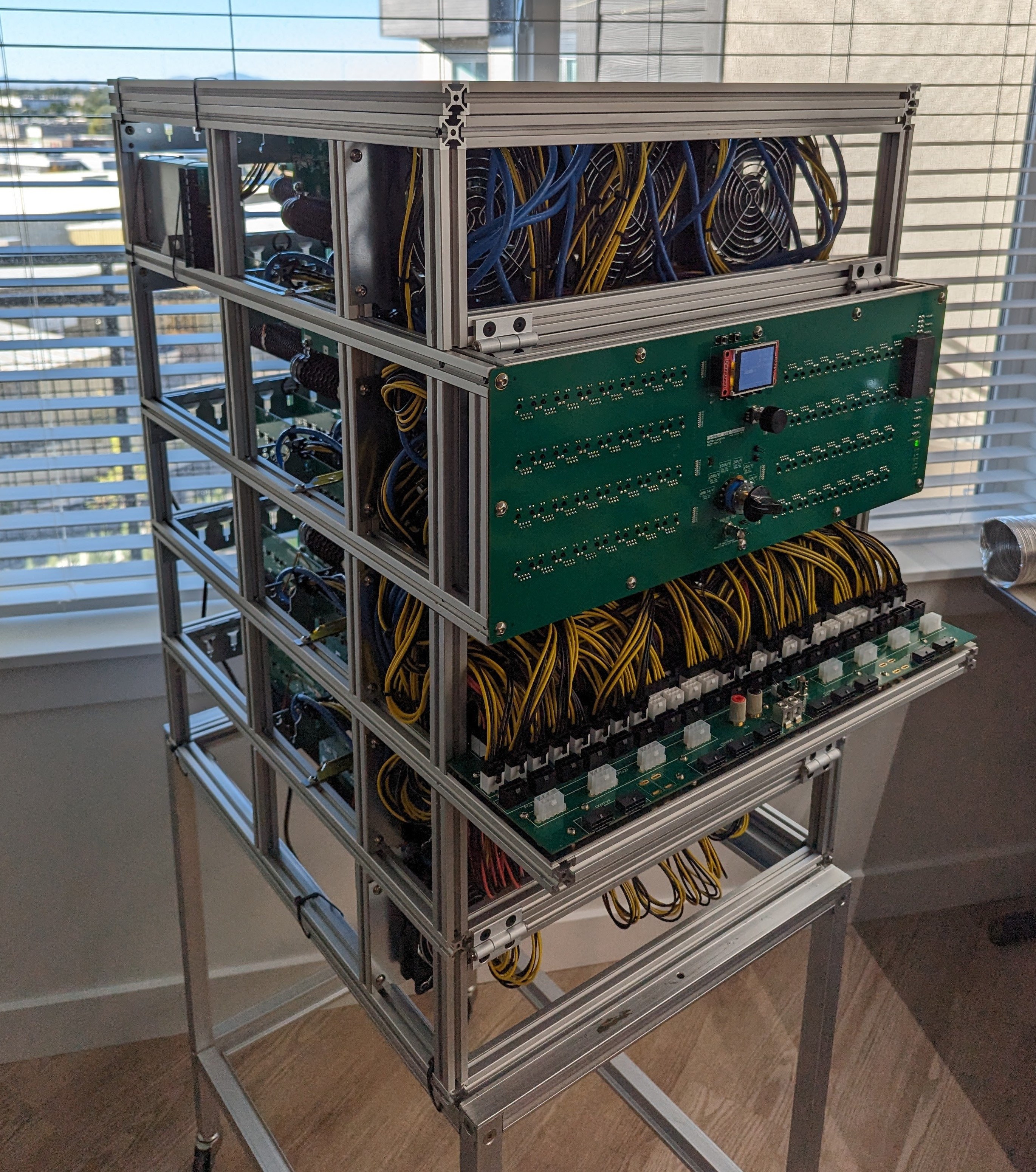
The End Result
The Plan

In principle it is simple: by connecting different combinations of binary value resistors in parallel, and assuming a constant input voltage, we can consume any arbitrary amount of current between just having the smallest resistor on and having all of them on. Implementing this gets much more complicated as current and pulse frequency rise.
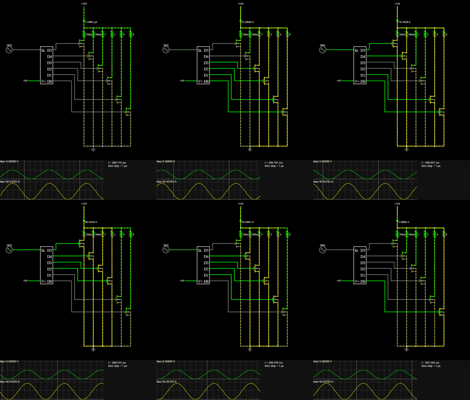
For my power supply testing application, I've targeted the following specifications:

  • Nominal 12.2V load input (3.3V-14.6V accepted)
  • 750A (9,150W) for one hour continuously
  • 1300A (15,860W) for 10 seconds
  • 2700A (32,940W) for 100us pulses (100us on, 200us off, 33% duty cycle at 3.3kHz)

Taking into account resistor tolerances and variation over temperature, the following resistor values were chosen to meet these specifications:


I'd initially planned on using mostly 1000W 0.25R resistors to make the bulk of the continuous load, however they doubled in price during design and so they are no longer cost effective.

Wanting a certain number of resistors switched in and out is a far cry from an actual implementation. How do you mount them? Wire them? Cool them? Control them? Prevent the switching FETs from getting damaged by the inductive spike on each turn-off? Nothing is ever quite as simple as it appears.

System Overview

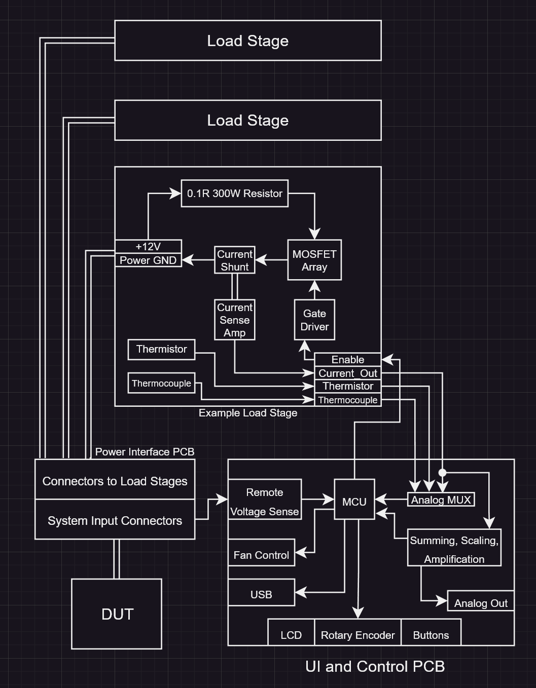
The system consists of four primary parts:

  • Load Stages - A single load resistor and it's associated switching and monitoring circuitry bundled in to one unit
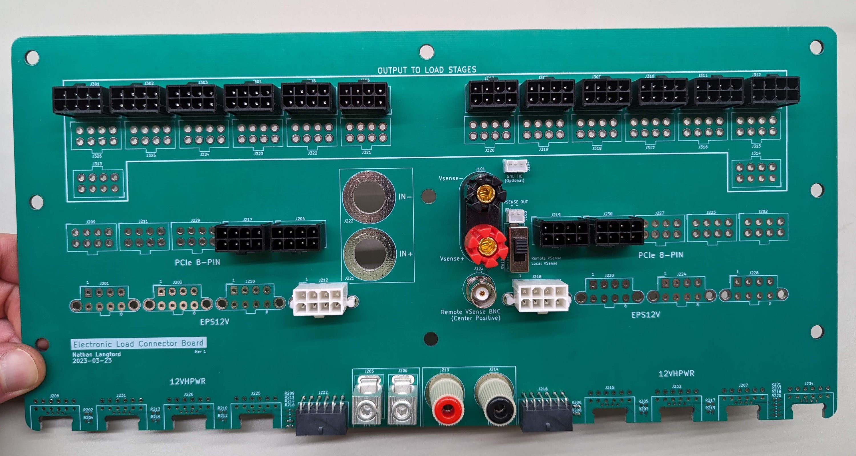
  • Connector PCB - Any power supply being tested (which I'll call the DUT - Device Under Test) connects to the Connector PCB. From here cables are run to each load stage to distribute power.
  • Control PCB - The brains of the operation. Takes input from the user, and enables the correct combination of load stages to produce the desired load. Monitors temperatures and current of each load stage, produces an analog output current signal for an oscilloscope, and much more.
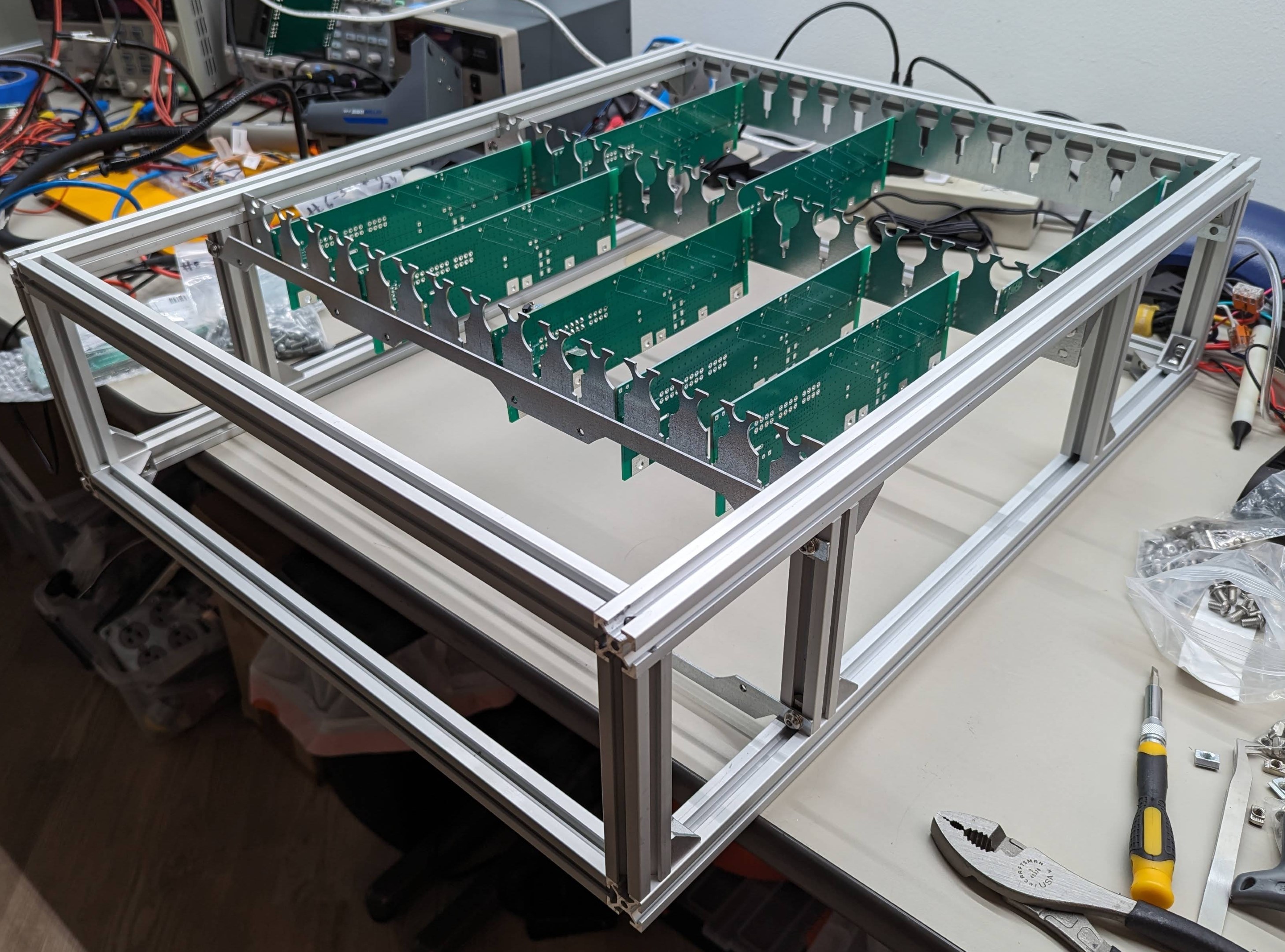
  • Mechanical chassis - Holds all of the load stages and other boards, provides fan mounts for airflow, and is designed to be backed up to a window so all the heat can be dumped outside.
Load Stages
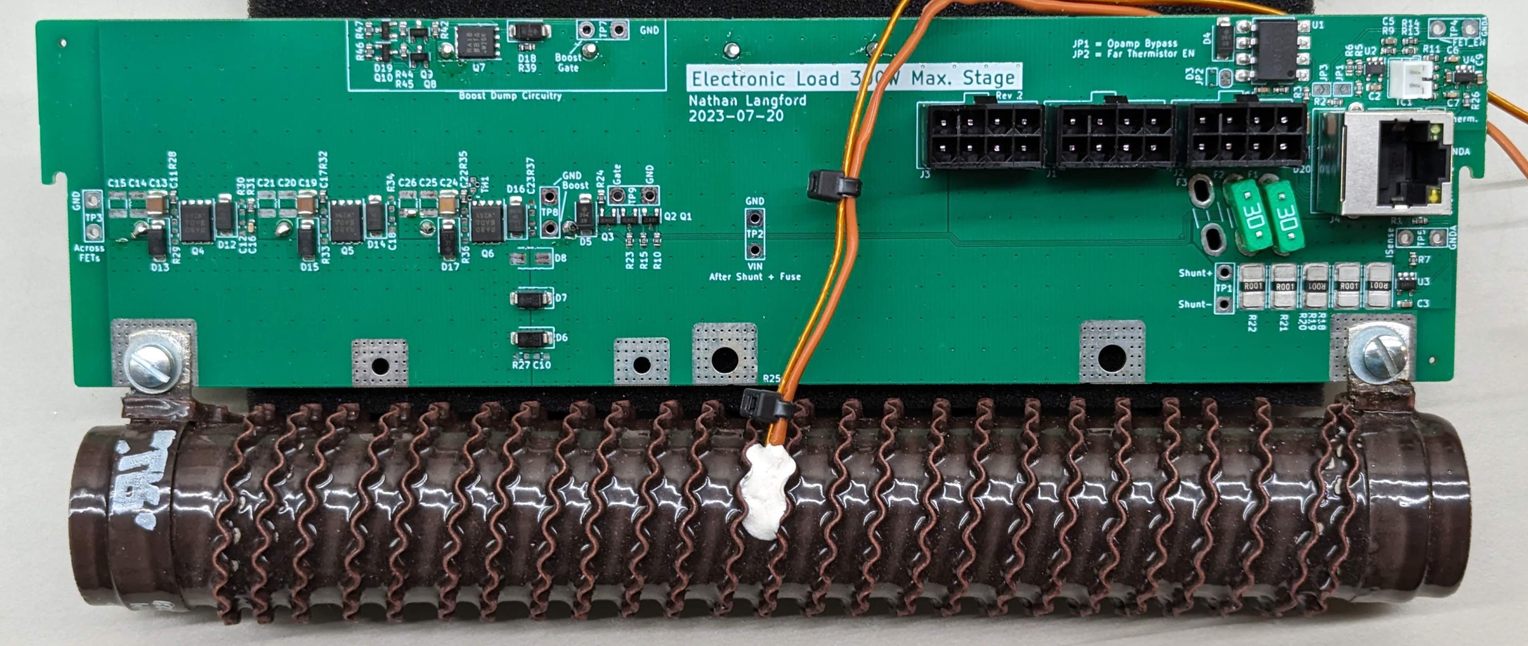
Each resistor will be attached to its own PCB to create what I'm calling a load stage. The load stages will all be connected in parallel to the system inputs. The load stages are self-contained and provide the following functions:

  • MOSFETs to enable the load stage to consume power.
  • Logic level input gate driver
    • Isolated to prevent ground loops
    • Using discrete components for lower cost
  • "Boost dump" circuitry to capture the energy from the inductive spike on turn-off, and dissipate it slowly.
    • When switching 122A repeatedly, the amount of energy stored in the inductance of the cables inside the system is large. Estimating 300nH total from the DUT in to the system, and then in to the load stage, that is 2.23mJ on each turn-off, or 7.37W at 3.3kHz. It gets even worse when you consider the inductance of the load resistor could be around 5uH. In simulation, this boost dump circuitry has to dissipate up to 30W when switching under a worst case scenario.
  • Current measurement
  • Thermocouple input and amplifier
    • For measuring temperature of the load resistor to prevent overheating, and potentially compensate for their temperature coefficient of resistance.
    • I'm actually using a INA180 current sense amplifier as the thermocouple amplifier. What cheaper way to get a 200x gain difference amplifier with very low input offset voltage?
    • I'm also making the thermocouples myself by spot welding thermocouple wire with a cheap Li-Ion battery-based spot welder intended for battery pack nickel strip welding.
  • Thermistor for software cold junction compensation of thermocouple

Since each load stage is completely independent, the system can be easily scaled down to 1 load stage (although you only get one bit of resolution of load this way: off and on), all the way up to the 64 load stages needed to...

Read more »
10kW Electronic Load Design Package - Part 2 - PCBs - 2023-10-10.zip

Control PCB, Connector PCB, Load Stage PCBs, and all associated manufacturing files

x-zip-compressed - 44.60 MB - 10/10/2023 at 12:00

Download

10kW Electronic Load Design Package - Part 1 - Everything except PCBs - 2023-10-10.zip

System BOM, build instructions, sheet metal files, 3D print files, CAD model

x-zip-compressed - 26.34 MB - 10/10/2023 at 12:00

Download

Control PCB 2023-08-08.zip

Schematic, KiCad Files, BOM

x-zip-compressed - 14.24 MB - 08/08/2023 at 07:37

Download

Mechanical Chassis 2023-08-08.zip

Assembly CAD STEP file, BOM

x-zip-compressed - 12.66 MB - 08/08/2023 at 07:37

Download

Connector PCB 2023-08-08.zip

Schematic, KiCad Archive

x-zip-compressed - 5.52 MB - 08/08/2023 at 07:37

Download

View all 6 files

  • Proof of Function

    tinfever10/10/2023 at 06:40 0 comments

    This is just going to be a few videos showing the fully assembled system in action. They are all going to be unedited clips, so I apologize if they are a bit slow. Consider these more as "proof of function" than education or entertainment. I'd recommend checking out the overview video in the main project details section, or the other project logs for more informative content.


  • Turning it up to 11...or actually 64

    tinfever10/10/2023 at 02:59 0 comments

    Picking up where I left off, the previous prototype with 8 stages was a success. It successfully demonstrated the principal of operation, and it also revealed areas needing attention. Building the full-size version of this project in a little over a month was really tight, but through luck, determination, and brute force, it has come through just in the nick of time (as I write this less than 8 hours from the deadline)

    A ton has happened since the last update with the prototype, so this is going to be a long post. Let's go!

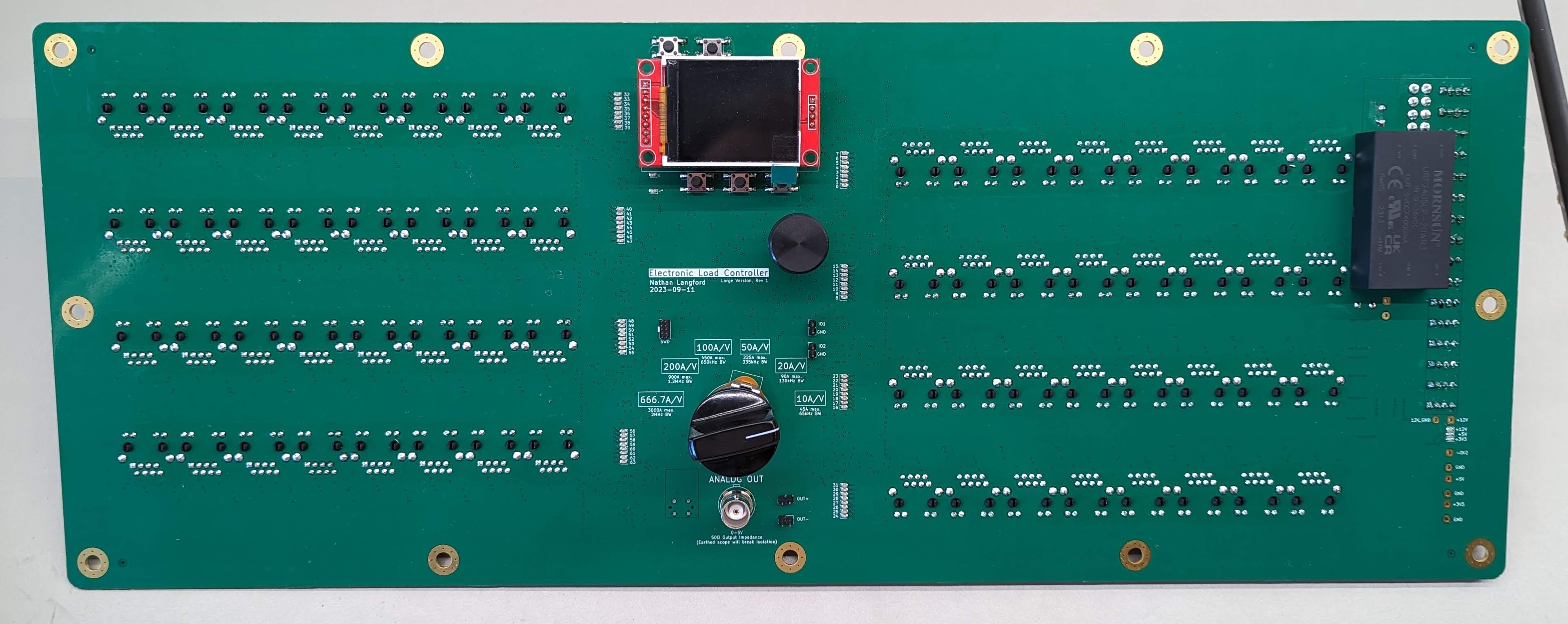
    Bigger and Better Control PCB

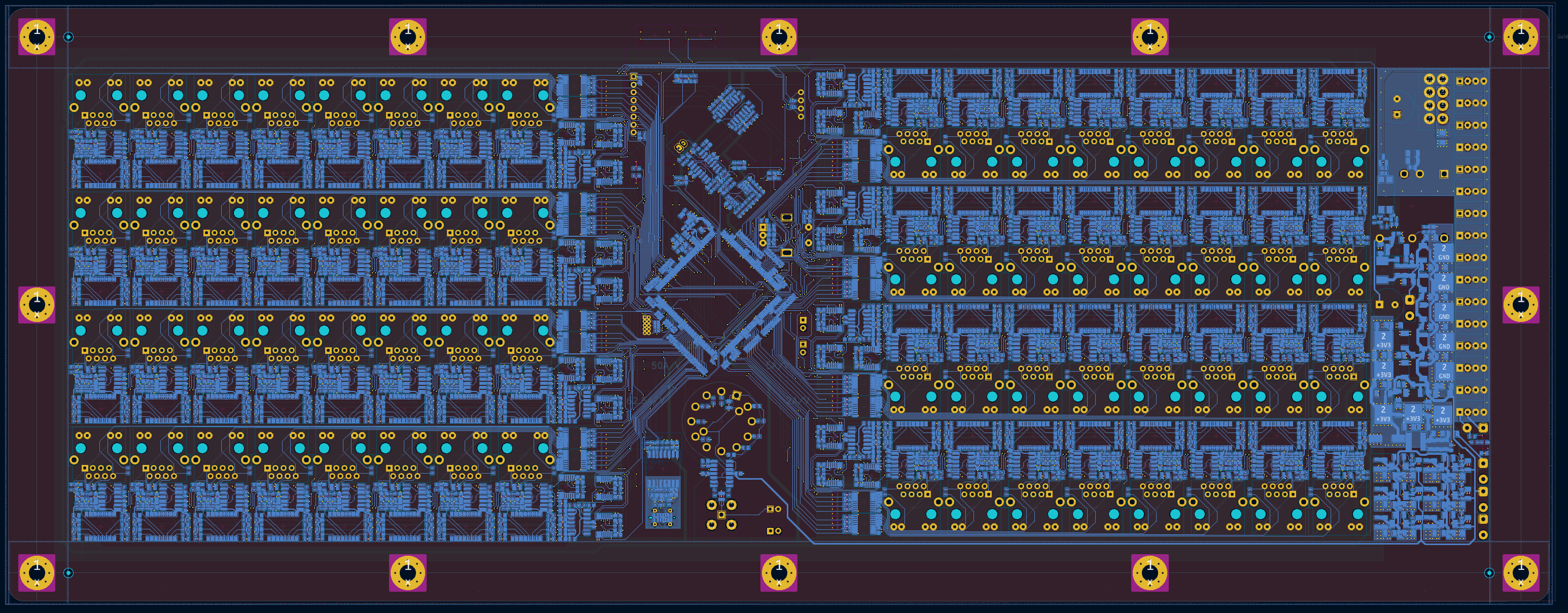
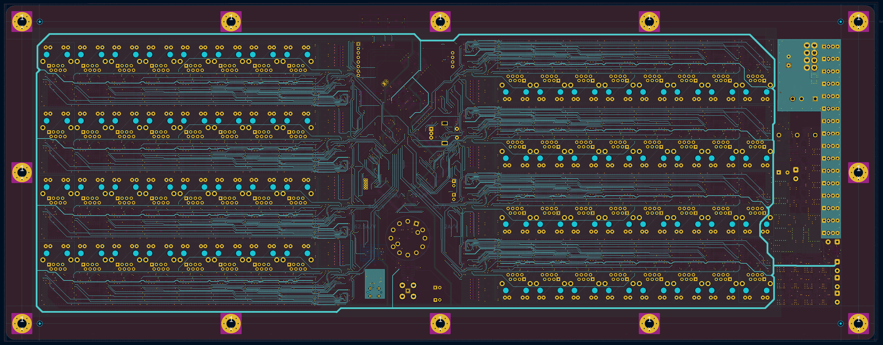
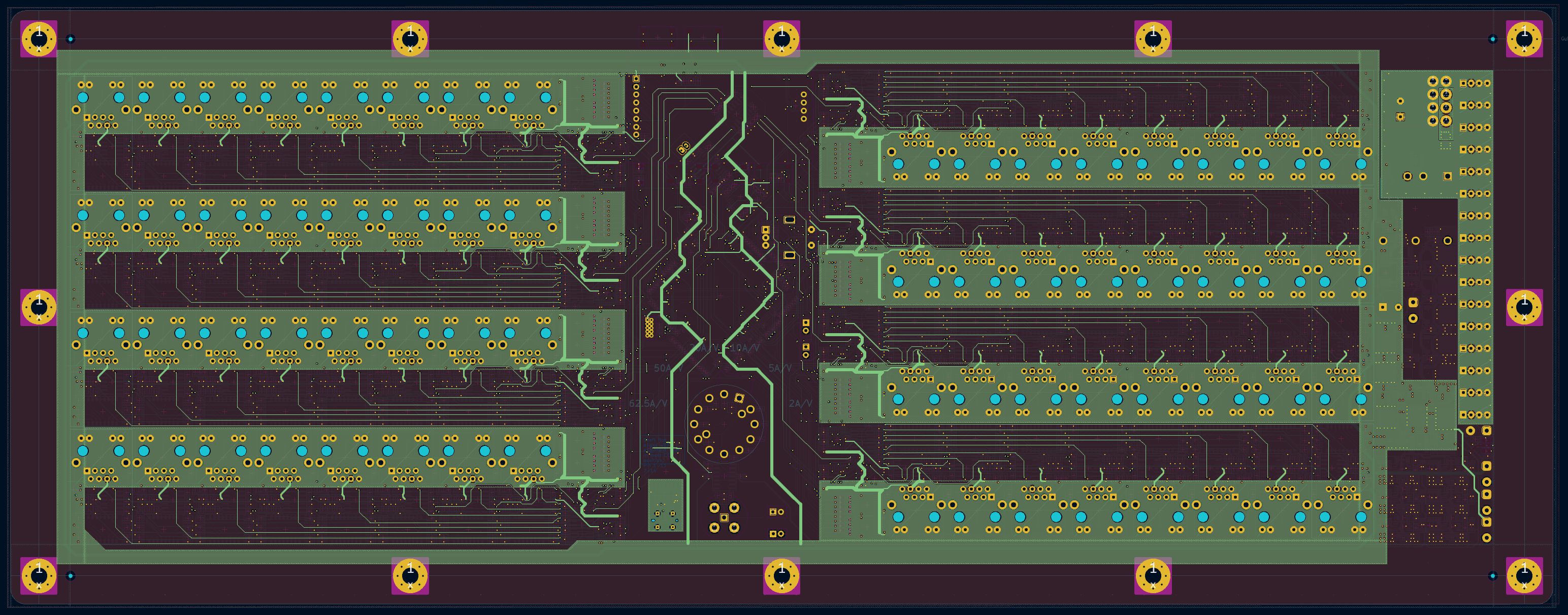
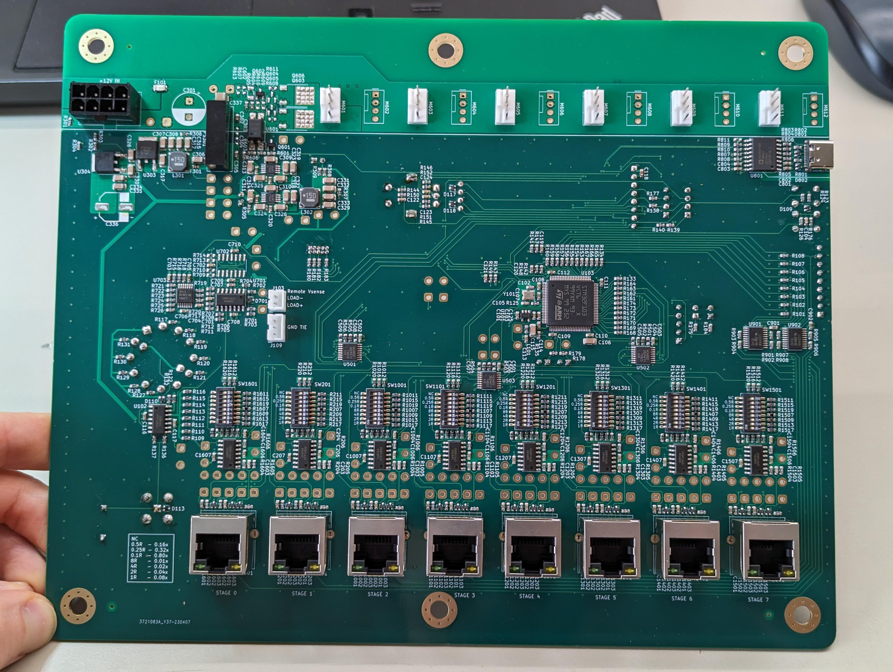
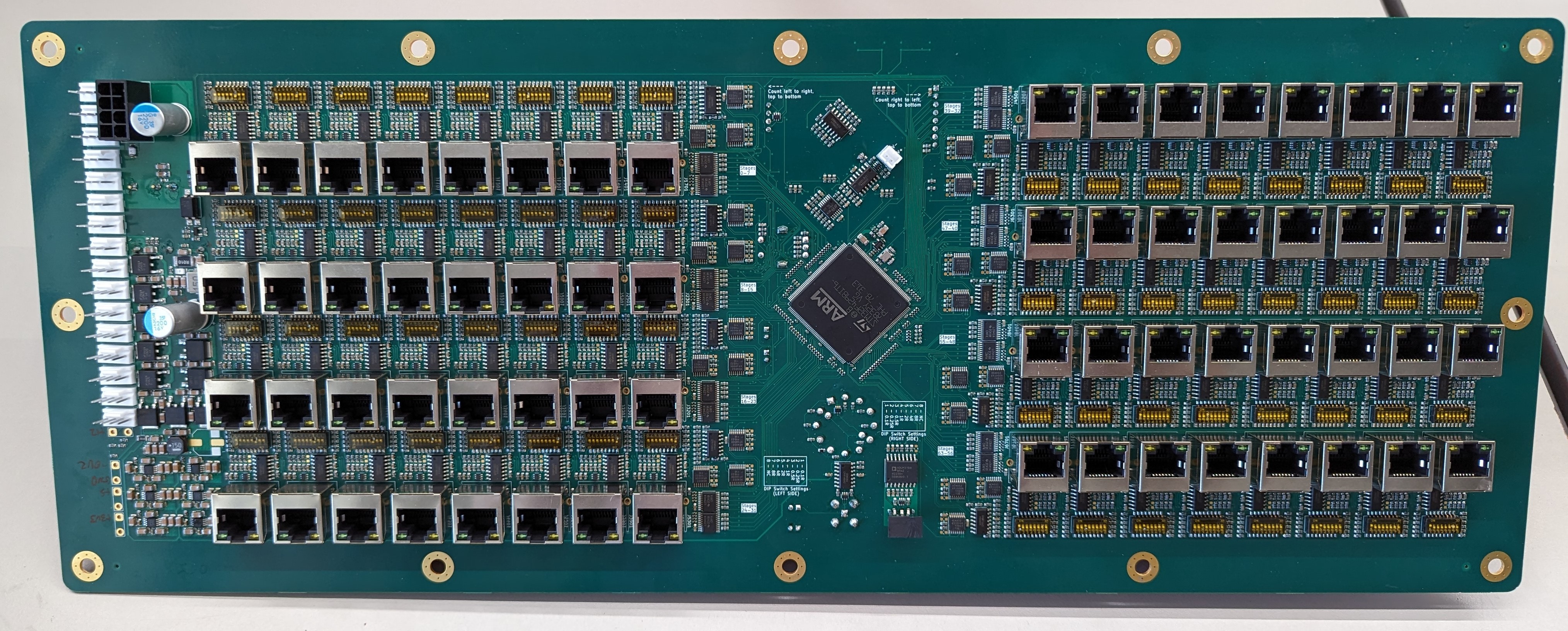
    The new control PCB is kind of a monster. Here are some highlights:

    • Supports 64 load stages (up from 8)
    • Upgraded microcontroller from STM32F103 to STM32F429, in one of their biggest packages (LQFP-208)
    • 6-layer PCB (three ground planes)
    • Same analog circuitry for each load stage as the prototype, just compacted and replicated.
    • Current signal analog summing now done in multiple stages for routing sanity and bandwidth improvements
    • Changed buffer ICs for straight through routing
    • Lower cost / more common TVS diodes

    This was a tight layout but I'm really pleased with how well it came out. Still, I had to take some shortcuts. There was no room for the isolated DC-DC converter on the back side, there was barely any room for test points on the PSU section, and some of the analog trace spacing is tighter than I'd like. I'd initially wanted to support 65 stages (13 per level x 5 levels in the chassis) but it quickly became clear that wasn't going to happen. 

    Back layer - containing as many of the digital signals as possible
    Layer 3 - Low priority analog, some acceptable digital lines like the MUX address lines, -0V2 power
    Layer 1 - Most sensitive analog signals (current sum signals), 3V3 power

    The primary reason for switching the microcontrollers was simply the need for more pins than were available in the STM32F1 family. I really wanted the enable signal for each load stage to have a dedicated GPIO pin, and for those to reside on mostly dedicated ports of the microcontroller. This is purely for speed, since switching the load stages in 100us pulses doesn't leave a lot of time to run shift registers. This way, I can directly write to the five GPIO ports where the enable signals reside and control all of the load stages in something like 10 clock cycles.

    I was also hoping to upgrade to a larger screen with touch input driven by a parallel bus but I had to cut that upgrade due to time constraints. I'm still holding out hope I might be able to bodge in a 3.5" SPI touch screen though.

    Why 64 stages?

    One thing I found working with the prototype was that the load stages all had a higher effective resistance than their nominal rating would suggest. (I may also throw around the term "conductance" in mA / V since that is how I wrote the firmware. See the firmware post for more details.) This resistance change only worsened as they heated up.

    Referring to the table below, you can see the cold (room temp.) and hot (200C) conductance values I measured in the load stages of the prototype. The 8R, 4R, and 2R stages were relatively accurate regardless of temperature. However, the 0.5R stages, and especially the 0.1R stages, were quite poor. A stage that would, in theory, be 0.1R, actually measured at 0.117R at room temp., and 0.130R when hot. I think the cold variation is from the cables and the connector contact resistance. While the hot variation is probably mostly the temperature coefficient of resistance for the load resistor.

    Either way. the conductance of the 0.1R stages could be reduced by over 23% from ideal, and the 0.5R stages reduced by over 10%. This was all made worse by the realization that the input voltage at the connector from the DUT was not going be 12.6V under heavy load. Between the droop designed into the power supplies (partially for load sharing), and the voltage drop over the PSU cables, the input voltage could easily drop to 11.4V.

    ... Read more »
  • Software eats the world

    tinfever10/10/2023 at 00:28 0 comments

    While not nearly as easy to photograph as other parts of the project, the firmware has been a big undertaking in the project, and it was my primary focus through August. 

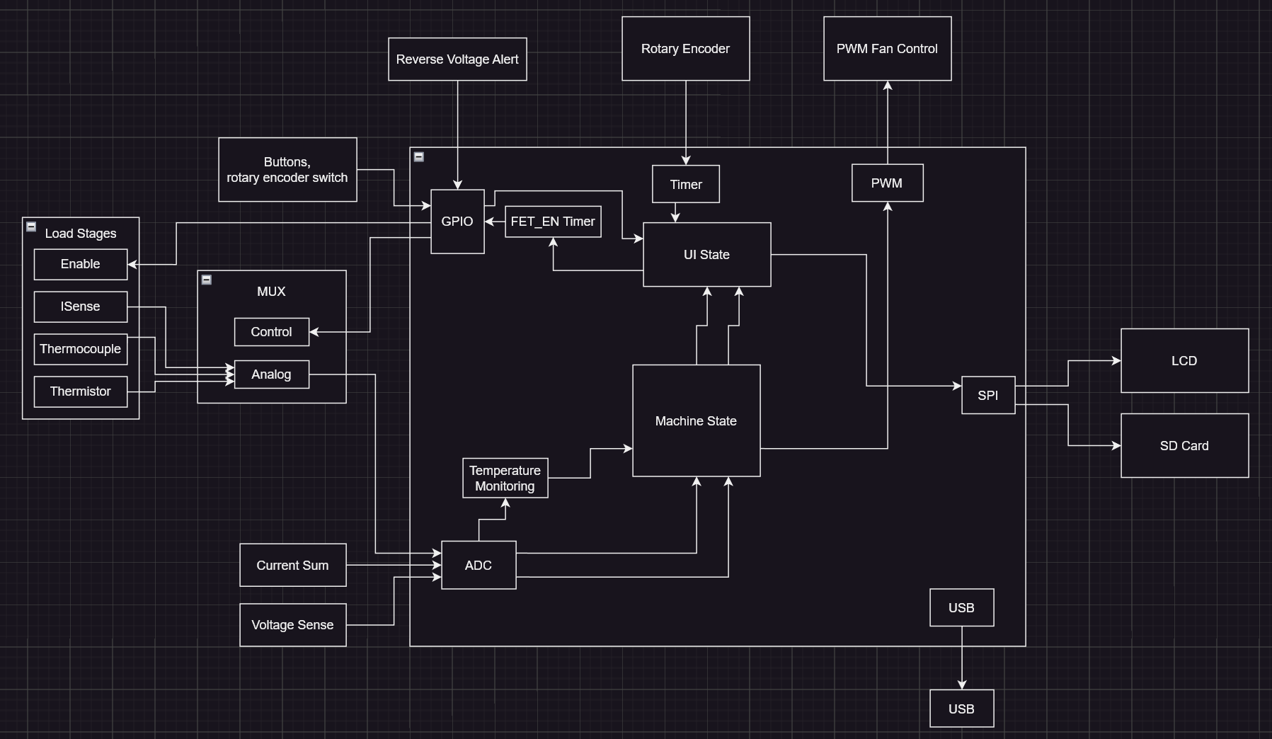
    An attempt at a software architecture block diagram

    The firmware has to manage a number of different things, many of which are somewhat interdependent:

    • Provide a GUI for the screen
    • Handle the buttons, and rotary encoder for the user input
    • Measure the voltage at the input and the current through the entire system (analog current sum)
    • Measure the current through each of the load stages
    • Sample the thermistor and thermocouple signals from each load stage and implement software cold junction compensation
    • Control the fan speed based on those calculated temperatures
    • Calibrate the load stage conductances
    • Solve for the optimal load stage selection for a given requested current
    • Rapidly switch the selected stages on and off during pulsed mode with precise timing

    (Regarding the software, you'll notice I use conductance instead of resistance. This is because the microcontroller can more quickly do a multiplication operation like "current = input voltage * selected conductance", instead of a division operation like "current = input voltage / selected resistance". Also, since there are multiple load stages being enabled in parallel, the conductances of each can just be summed together. Compared with the "inverse of the sum of inversed resistances" calculation you'd do to calculate the equivalent value of multiple resistors in parallel, which is actually just converting them to conductances and back anyways.)

    Control Algorithm Overview

    (More details for each point below)

    • On startup, the conductance of each load stage is measured and stored
    • When the user requests a specific current value, the input voltage is measured and used to convert that to a target conductance
    • An approximate solution to the subset sum problem is used to determine which load stages should be enabled to get as close as possible to the target conductance, and thus target current.
    • This solver is run every 50ms, so any change in input voltage results in a new target conductance to maintain the same current target.
    • While a stage is enabled, it's conductance is regularly measured on-the-fly to take into account temperature variations. This live measured conductance is used for the next subset sum calculation.

    Subset Sum Problem

    One interesting thing I found early on, is that I've apparently have run head first into the Subset Sum Problem. Essentially, there are many different load stages each with a different conductance (mA / A in my firmware). The current value requested by the user is converted to a target conductance using the input voltage, and then the software needs to determine which subset of all possible load stages should be enabled to get as close as possible to that target conductance without going over. Going over would mean drawing more current than the user requested, which might be considered a bad thing in some scenarios.

    It turns out that this is a fairly fundamental problem in computer science, and there is no perfect and fast solution. If I had only 8 load stages, I could easily pre-compute the sum for all possible 256 combinations. However, if I have 64 load stages, that's over 18 x 10^18 combinations, so there is no chance our little microcontroller could even store all of those, let alone compute them in under three years.

    Fortunately, in this case there is a simple approximate solution, the "Simple 1/2-approximation". Essentially, the firmware just has to take a list of all of the load stages sorted by conductance, select the largest one that fits within the target conductance, then subtract the selected stage conductance, and finally repeat the process with the remaining amount. If the load stages were perfect binary values of each other, this actually would be an optimal solution. However, this leads to another issue: the load resistors have a tolerance of 10% and...

    Read more »
  • Can't stop the work

    tinfever08/06/2023 at 03:45 0 comments

    This is just going to be a quick update post showing off everything that's happened since the last post. Cue the pictures!

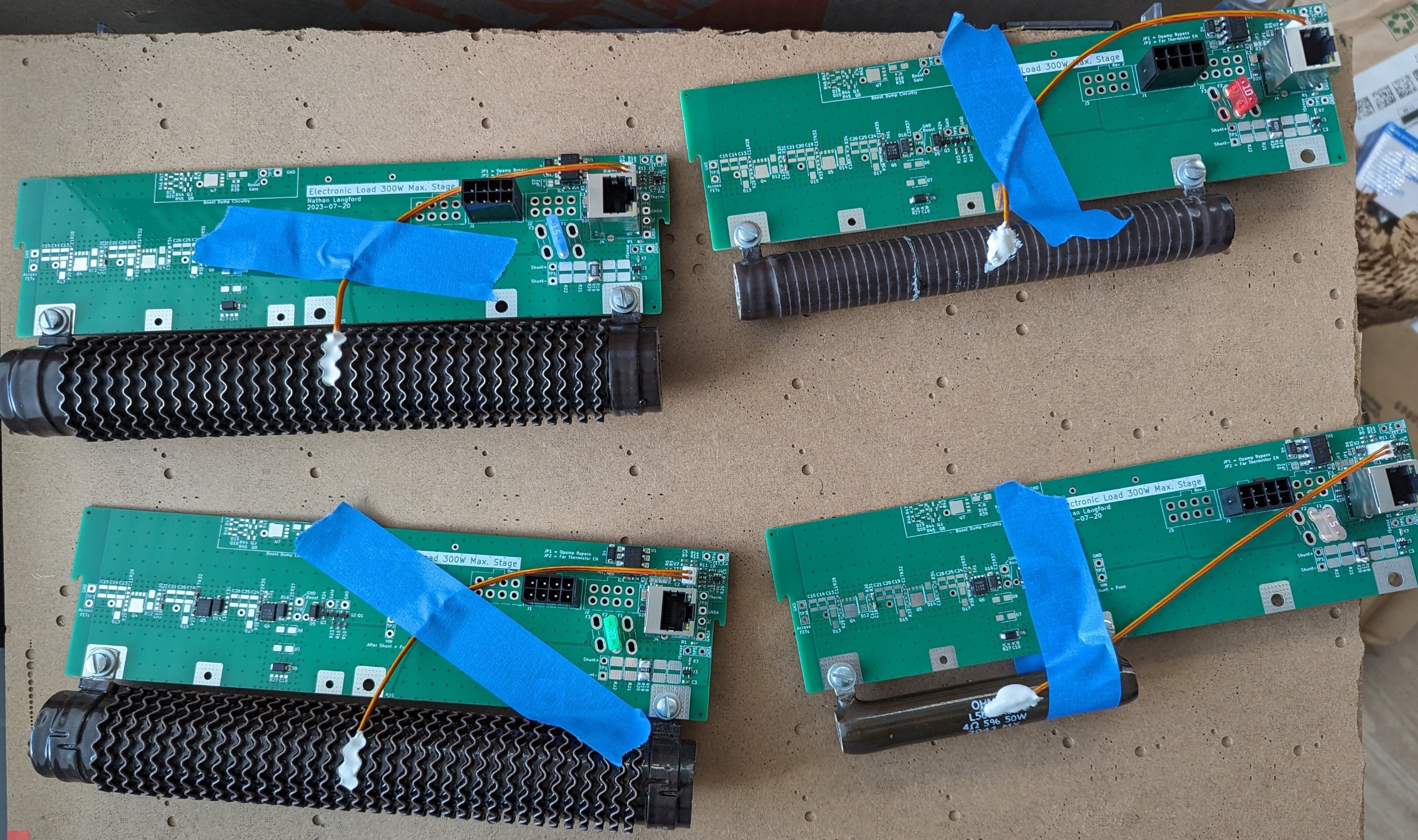
    The new load stages PCBs arrived. These feature:

    • Updated optocoupler circuitry to greatly reduce turn-off delay.
    • Switched to using MINI blade fuses, sometimes in parallel, to reduce cost dramatically. Those previous MAXI fuses could be nearly $3 each, and the MINI fuses are around 0.08$ each!
    • Relocated the capacitor Cgd on the FET to be as close possible. Also, added series resistor with it to dampen the oscillation it caused. (Kind of feels like a dirty hack but it works...or at least now I can't see it)
    • Added thermal reliefs to all the through-hole parts. Last time I discovered they are definitely not optional. I might need to make them even thinner next time since those PCIe connectors are still hard to solder and need a pass from each side of the pin. They are going directly in to solid planes though.
    • Moved the gate driver transistors much closer to the FETs.
    • Switched to a different TVS diode type to align with the PCB assemblers preferred parts (and they are just cheaper and just as good otherwise)
    • Added a series resistor to the NPN push transistor in the gate drive. This allows input voltages to go higher than 14V without quickly being at risk of burning up the FET gate protection TVS.
    • More optimized gate driver pull-up transistors to reduce quiescent current consumption
    The whole family all together. Showing all six variants: 8R, 4R, 2R, 1R, 0.5R, and 0.1R.

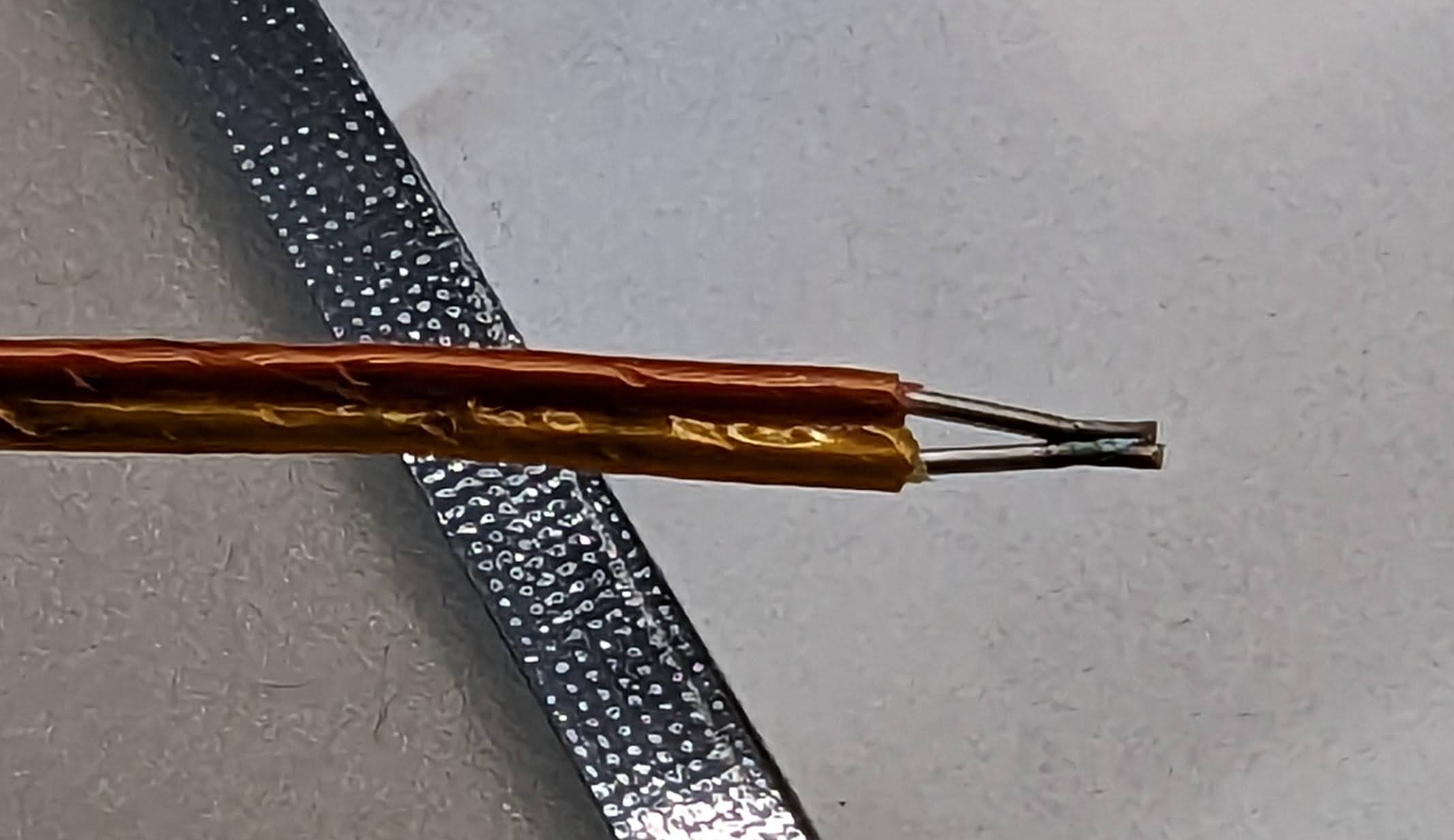
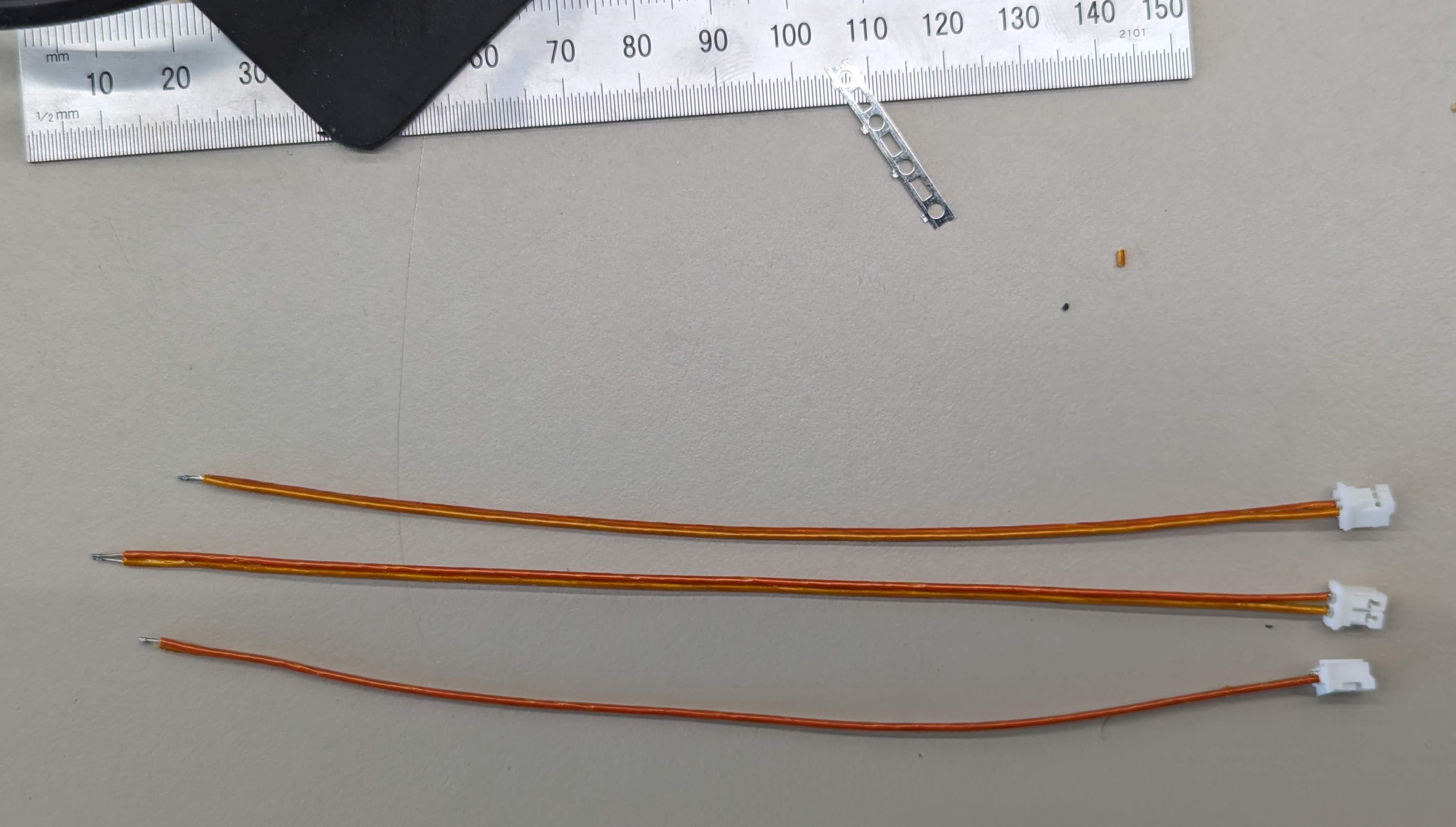
    Thermocouples have been DIY spot welded, crimped, and epoxied to the load resistors. The thermocouples will someday get their own post but I'm using a cheap Li-Ion battery based spot welder intended for welding nickel strips when making battery packs. It works pretty well for this. The epoxy has to be a special high-temp cement (CC HIGH TEMP from Omega) to survive the 250C+ of the load resistors. I tried JB-Weld first a while ago but that just becomes soft and falls apart at those temperatures.

    The welds aren't all this pretty.
    Ready to epoxy (or is it really cement?)
    Curing for 24 hours

    Main Control PCB Assembly 

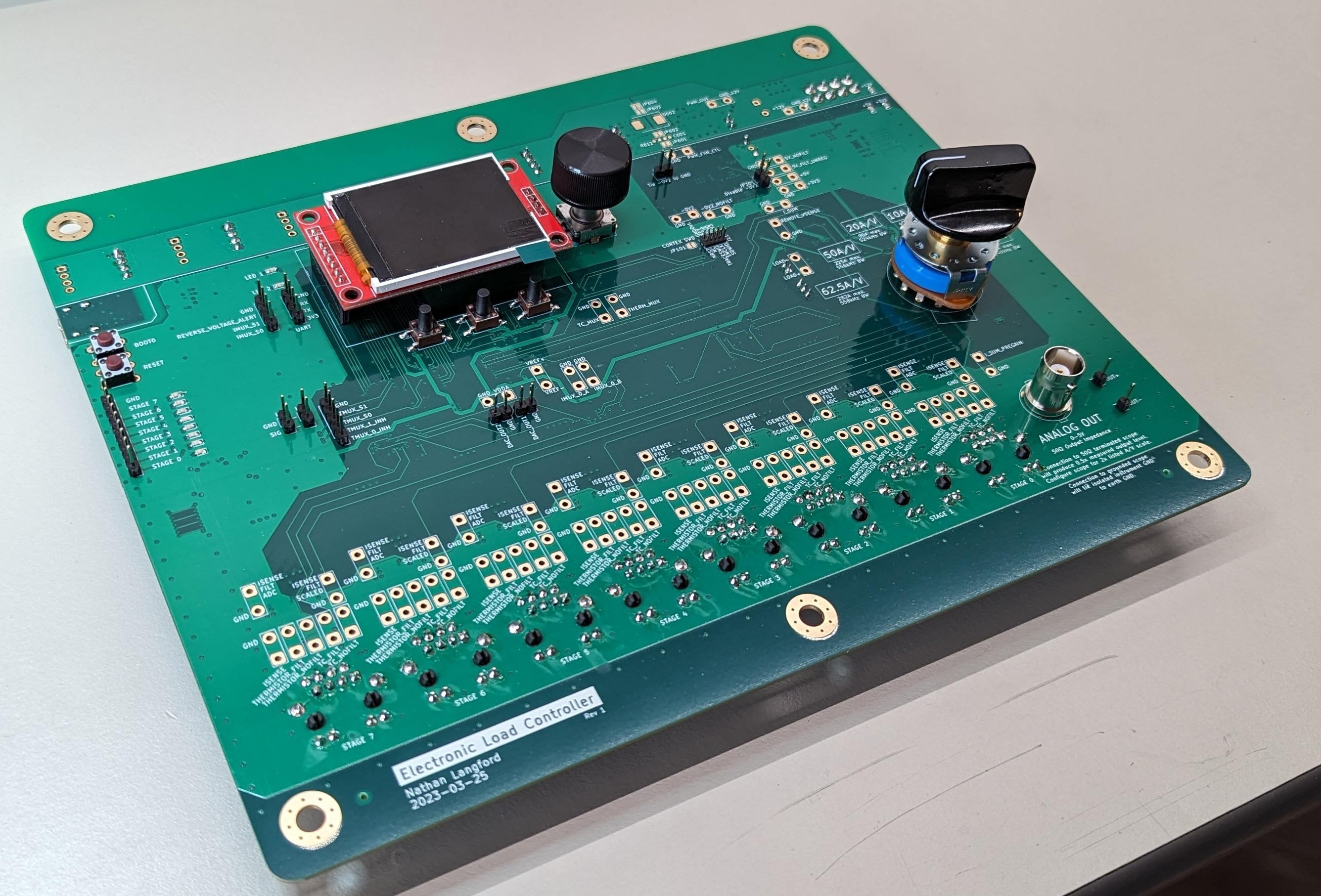
    The control PCB has over 570 components on it, which was rather painful to pick and place by hand. I timed myself and it took me almost exactly 5.1 hours to place the 511 SMD parts on the back. So I can do about 100 parts per hour. Not great, but there is a high component mix with 65 unique parts on the back. This whole system I'm working on right now is the prototype so the control PCB only supports 8 load stages. If all goes well, a future version will support the 50+ needed.

    Front
    Rear. It's so beautiful!

    Connector PCB Assembly

    This board has the job of taking in power from the DUT and distributing it to all of the load stages which operate in parallel. It also provides a remote voltage sense signal for the control PCB. It's only partially loaded here to support the max current levels I'm expect to hit on this prototype. The binding post solution on this is pretty weak since it's clear to me these were designed for panel mounting and not an electrical connection to a PCB. 

    Putting together the mechanical chassis

    Here is the first level of the chassis. Like everything else in the project, it's designed to scale to multiple levels. Each level can hold 13 load stages and three 120mm fans. I'm not sure what possessed me to use PCB hooks as a mounting mechanism for the load stages. It'll work because the whole thing is stationary but otherwise not a great solution. I suppose it is cheap though!

    Including some blank load stage PCBs to get the spacing right

    Putting it all together

    This has the second load-stage chassis level installed which also provides the mount for the control PCB. There is an extension of the chassis the sticks out the front for the connector PCB to mount to. The connector PCB has to overhang that a bit to support the right angle connectors on the front edge as well as the binding...

    Read more »
  • Why design a discrete gate driver circuit?

    tinfever07/25/2023 at 00:13 0 comments

    While waiting for the load stage rev 2 PCBs to arrive, I'll share some of my thought process in deciding not to use an off-the-shelf isolated gate driver IC on the load stages. Switching the power to the load resistors is arguably the most important part of the entire design, and so a lot of work went in to designing, simulating, and testing it. (The second most important part is probably everything that keeps the inductive spikes from blowing up the MOSFETs.)

    Tl;dr: I like making life harder for myself, I'm a terrible cheapskate, and my questionable goal to work down to 3.3V on the DUT's power supply eliminates essentially all off-the-shelf solutions.

    Here is the deep rabbit hole I went down again in recently reevaluating the design and deciding not to use an off the shelf isolated gate driver IC with some real reasons, and some retroactive rationalizations:

    • It should be cheaper to do a discrete solution (as long as I don’t value my time...), and if I need 50 load stages, costs start to add up. A $1 part adds $50 to the system BOM.
    • I thought it would be more challenging, and I seem to like making life harder for myself.
    • Most isolated gate driver ICs have an output power supply requirement of 10V+. Since I’m powering the gate drivers from the DUT’s power supply, this would mean the load stages might not work at lower input voltages. 
      • There are some with a lower output VCC minimum like 4.5V like the IS480P or FOD8480 that look like they might work but now we’re at $0.93 or $1.67 each respectively in 100 qty.
      • Also, 4.5V is still higher than I’d like if I want the system to work down to 3.3V DUT input voltages.
    • If I want to turn off the MOSFETs quickly to minimize power dissipation during switching (only for the 0.1R 122A load stage does this matter), I need the driver to be able to sink a decent amount of current.
      • IS480P looks like it can sink 160mA+ so that would probably be fine. FOD8480 could sink 80mA which may or may not be enough.
      • If that isn’t enough current, then I need to follow the isolated gate driver with a BJT push-pull buffer. However, that then means that my max gate drive voltage is limited by the logic output high level of the gate driver IC. The parts I just mentioned can both swing somewhat close to VCC so that wouldn’t be an issue I think.
    • Isolated gate driver ICs seem to have fairly high quiescent current draw.
      • IS480P has a supply current of 1.9mA typ. to 3mA max. FOD8480 is similar at 1.6-2.5mA.
      • Since the gate drivers are powered by the DUT, and there will be 53 load stages, 3mA each means 159mA drawn from the DUT whether the load is enabled or not.
    • If operating with an input voltage of 3.3V is a hard requirement, I don’t see a single isolated gate driver part that can operate that low on the first page of a Digikey search, with Voltage - Output Supply filtered to have a minimum at or below 3.3V.
      • This is probably for a sane reason: the threshold voltages of many MOSFETs might be around 2.5V, so there would not be much margin to work with. I never claimed my requirements were completely sane though...
    • You'd think an IC would be able to have lower quiescent current draw but since I don't care about the turn-on time at all in my application, I can use high value pull-ups to minimize the quiescent current and come in little lower than an IC.
    • The best, more integrated solution would probably be a logic output optocoupler like a TLP2361, followed by a BJT push-pull driver stage. It can operate down to 2.7V VCC, with a supply current max of 1mA. However, its max VCC voltage is 5.5V, which is a problem. Interestingly, the inverting version, TLP2358 can operate 3-20V. So now we need to use the TLP2358 and follow it with an inverter, and then the BJT push-pull stage. This inverter output has to swing to at least 11V if we want to be sure we can drive the MOSFETs gate above 10V to minimize Rds losses, that’s going to be hard to find, and then we’ll also have to add additional regulation to make sure the inductive voltage spikes...
    Read more »
  • New Optocoupler for Gate Driver

    tinfever07/14/2023 at 18:23 0 comments

    Two posts ago I discussed the need for a faster optocoupler than the LTV-816S I was using before, and I mentioned the 6N136. Here’s why I selected that part:

    How can you argue with that?
    • It was the first and most common result when searching for optocouplers on Digikey with transistor output, turn-on time less than 1us, and sorting by price.
    • It’s a common component available from multiple manufacturers
    • It was mentioned online as a faster alternative to slow phototransistor-based optocouplers.
    • I probably have a tendency to see a part / get an idea and run with it, rather than evaluating all the options first. Which is kind of how I got sucked into this project in the first place...

    Here’s the design I’ve settled on:

    This has a few changes from the last design to accommodate the 6N136:

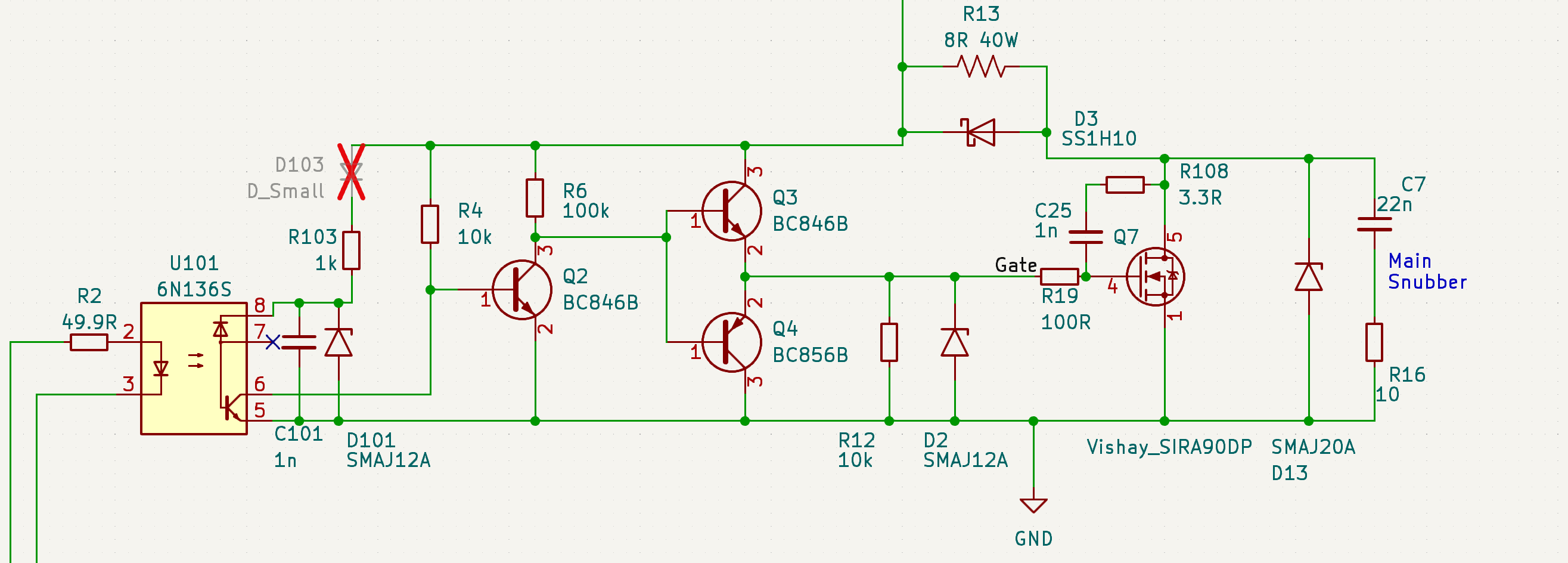
    • It requires a higher drive current, so the input resistor is now 49.9R, combined with 49.9R series termination resistor on the control PCB, that should make the drive current 14-19.7mA depending on the Vf of each optocoupler.
    • It has a max VCC voltage (pin 8) of 15V. Inductive spikes can cause the load stage input voltage to go up to 25V on a 12.2V input, only limited by the existing slew rate control circuitry and TVS diodes. I added a 12V TVS to VCC on the optocoupler with a 1k current limiting resistor to address this. This should clamp VCC to below 15V, and the supply current is minimal so the 1k is no problem otherwise.
    • It needs a decoupling capacitor across its VCC and GND pins. I initially thought I might be able to get away without this, but testing showed it really is needed. I was getting an unusual oscillation of the gate drive on turn-on that went away when I touched the VCC pin, so the capacitance of my finger is all it needed in that case. The oscillation was most prevalent when switching higher currents, or when the cable inductance was increased.
    Touching the VCC pin is all the capacitance needed to fix the instability. This obviously doesn't scale though...
    • The output pullup resistor was changed from 3.3k to 10k. Performance was satisfactory with the 10k, and it reduces the load stage quiescent current from the DUT to 1.3mA. This matters when there are 53 load stages.
    • The pullup for the BJT inverter after the optocoupler was changed to 100k from 1k. This dramatically reduces the quiescent current. The resistor determines how much current the BJT push-pull driver stage can source during turn-on. However, for the turn-on transitions the gate driver speed doesn’t actually matter at all. The inductance of the load resistors is always the limiting factor, not the MOSFET turn-on speed. The turn-off transitions matter much more (and even then, only on the highest current 0.1R 122A load stages).
    • I’ve added an optional diode in the VCC supply for the 6N136. I’ll probably just short this out but it leaves me the option to place it later. Any capacitance across the load stage supply is a large problem, because when the load stage turns off, the inductance of the load resistor and cables causes a voltage spike. This voltage spike causes any capacitor to get charged above the voltage of the DUT, so once the spike is clamped and the voltage comes back down, the capacitor is discharged back in to the DUT, forcing it to sink current. How much current can a power supply sink safely? I have no idea. I even wanted to eliminate the RC snubber across the MOSFET for this reason, but I don’t know of any other way to get rid of the ringing of the cable inductance and FET//TVS capacitance. The diode will prevent this added capacitor on the 6N136 from discharging this way, although the 1k resistor reduces the magnitude of the current going in reverse, even if the actual charge amount is the same.

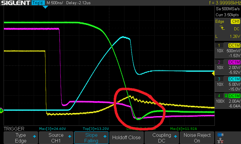
    Green is the current flowing through load stage. See that dip? That's *negative* current, or current being forced from the load stage back in to the DUT due to the RC snubber. (Yellow = FET_EN, Blue = Voltage drain-source on FETs, Purple = Gate Drive...
    Read more »
  • Already finding weird behavior in other things...

    tinfever07/14/2023 at 03:18 0 comments

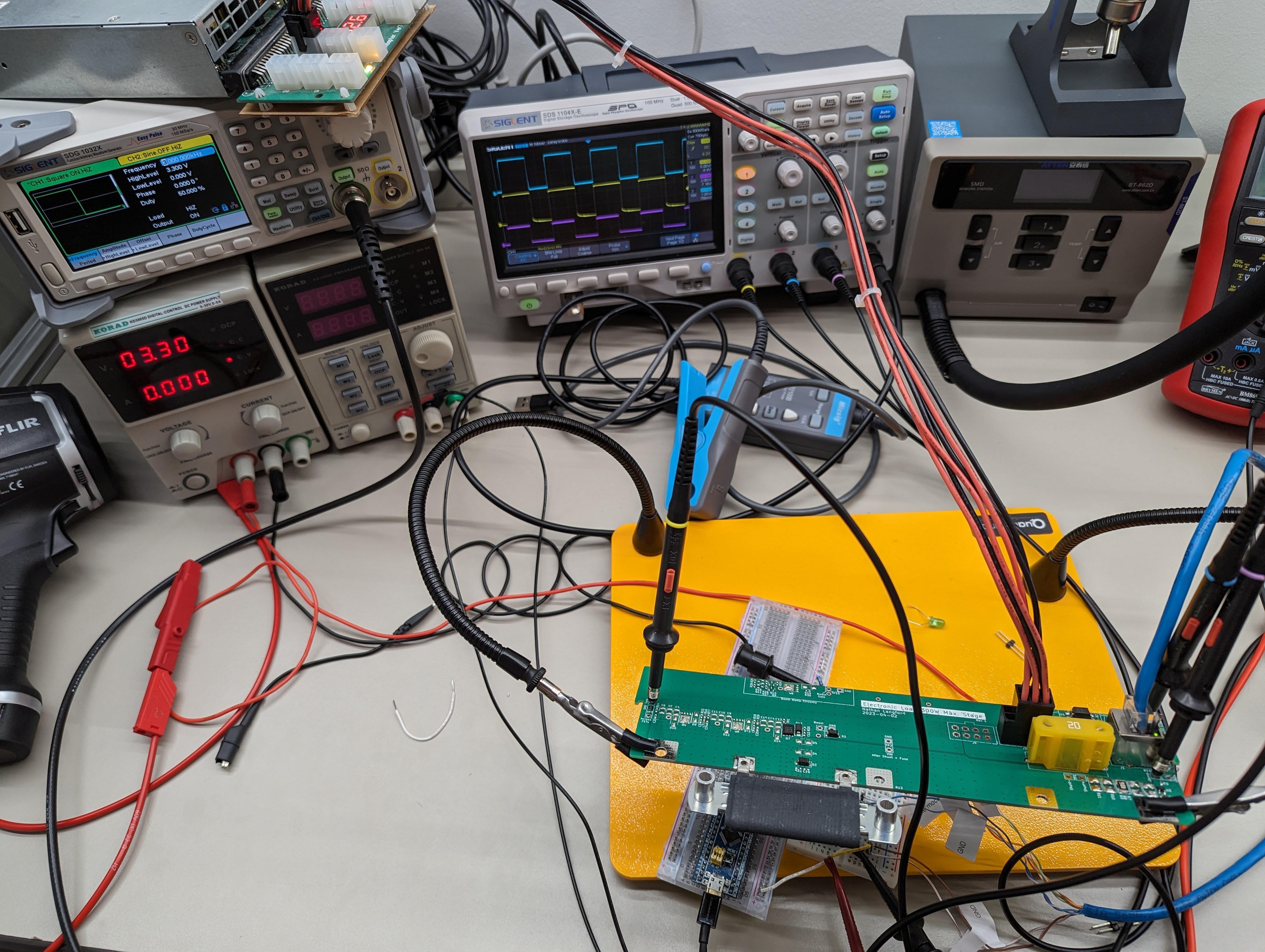
    I was testing the load stage at higher currents today after installing a second MOSFET on the PCB to support a 0.5R load resistor, when I ran in to some bizarre turn-on behavior.

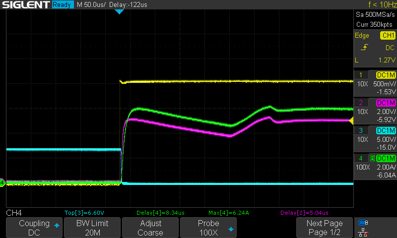
    That's...not supposed to happen. Yellow is the FET_EN signal, Blue is the voltage across the FETs, Purple is the gate drive output to each FET, Green is the current through the load stage. This is on a 1R load resistor with a 6V supply from my bench PSU

    At first I feared this might some complex interaction between the two MOSFETs. Could they somehow be turning on at different times and causing some weird feedback? But why would the current track the change in voltage if it isn't going below the FET threshold voltage? Is the 100k pullup driving the BJT push-pull gate driver stage not enough? I've really gone too far this time.

    I started probing around as well as varying the frequency and pulse width from the signal generator:

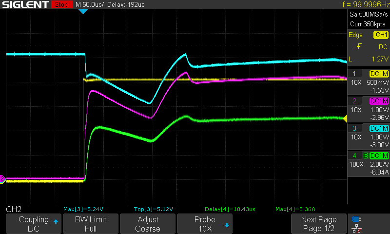
    Now the blue trace is the voltage applied to the load stage

    What madness is this? I'd expect the voltage across the load stage to drop a little as the current increases due to the resistance of the cables, fuse, current shunt, etc. You can even see this happening at the very start, but then they start to become correlated. The input voltage drops and the current drops simultaneous...what?

    The only thing that would make sense would be the... power supply.

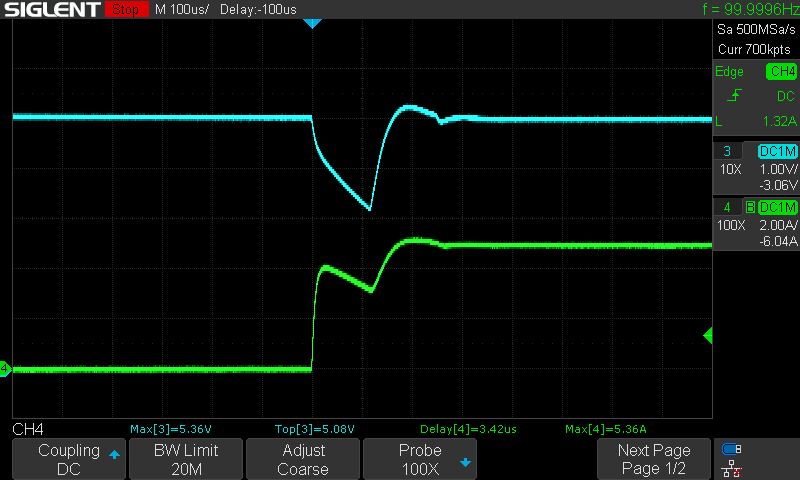
    Green is the current through the load stage, Blue is the voltage measured at the bench power supply terminals

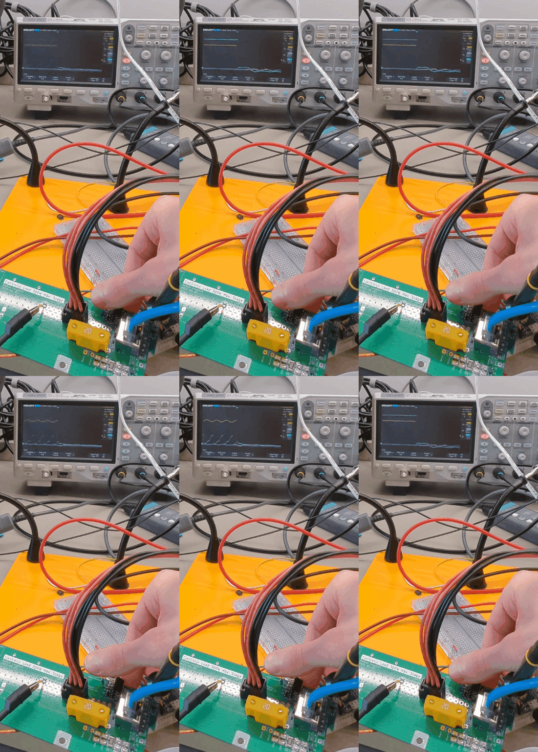
    Yup. The bench PSU is messing with me. Both of them, in fact. I have a Korad KA3005P and KD3005D that both show the same behavior. I'm not sure if it's the rapid change in current, or the somewhat inductive load, or something else. I'm just glad this isn't my problem this time!

    I switched to the server PSU I'm using for a lot of this testing since it can supply 100A at 12V and the issue went away.

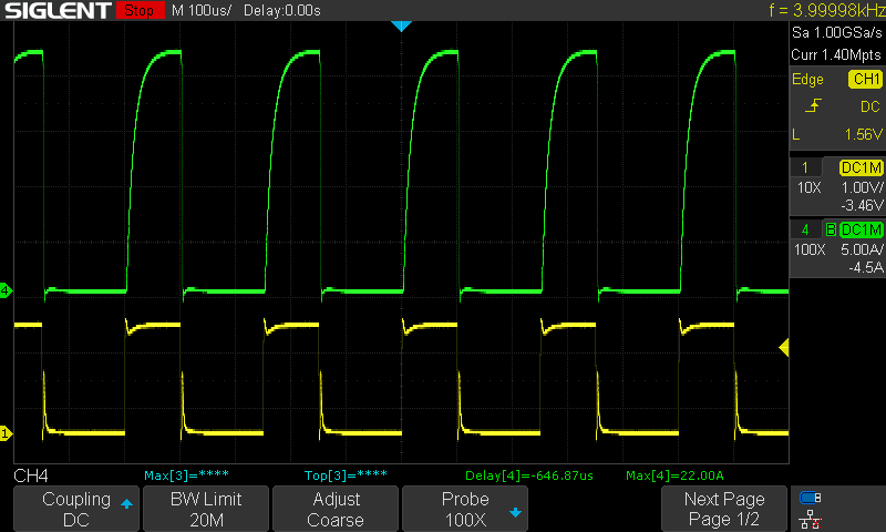
    Yellow is the FET_EN signal, Green is the current.

    Looks at those beautiful 22A 100us current pulses! You can clearly see how the inductance of the 0.5R load resistor is limiting us here. Pay no attention to the ugliness of the FET_EN signal. I think that's caused by current actually flowing back through the scope's earth connection to the PSU, since ground isn't ground when you're swinging this much current around over cables. That'll have to be its own blog post.

    In case anyone is keeping tracking, this means the 8R, 4R, 2R, 1R, and 0.5R load stage configurations are working successfully, which covers a current range of 1.5A to 25A respectively. Tomorrow I'm going to assemble a 0.1R load stage that has to work at 122A, that's where things get serious.

  • Turn-off delay investigation

    tinfever07/13/2023 at 18:41 0 comments

    Let’s take a look at that turn-off delay issue. 

    Yellow is FET_EN, Blue is gate drive output. Turn-off delay is 28-32us depending on test conditions.

    If my goal is to be able to do 100us pulses, having a 30us turn-off delay is a problem. The timing is fairly critical because I need all of the load stages to switch at the same time, more or less. I’d also like the option to precisely sequence the load stages to either control the DUT current slew rate, or to compensate for the higher inductance load resistors which have a slower current slew rate by turning on some of the “faster” low inductance stages briefly. I think I’d like the load stages to respond within 5us, and ideally faster.

    After more learning and research, I think I’ve determined the root cause. In short, I picked a cheap and slow optocoupler with phototransistor output, the slow kind. (PN: LTV-816S)

    I didn’t read the datasheet closely enough and was relying on the listed 3-4us response time, but I didn’t pay attention to the test conditions. They actually specify that response time with a V_ce of 2V, an R_load of 100R, and I_c of 2mA, which actually means they are measuring a voltage swing of 200mV around a 2V signal. Definitely not the 0-600mV swing needed in my design to switch the following BJT inverter. Also, I was using an output pull-up of 3.3k which made things much worse.

    I think the fact that I'm pulling up to a higher voltage (12.2V assumed from DUT) and then clamping the output with the following BJT inverter is actually helping me do better than these numbers.

    I recreated the optocoupler and inverter section of the gate drive circuitry on a breadboard and used that to confirm the issue. Although, I could pretty clearly see how long it was taking the optocoupler output to rise measuring in-circuit on the load stage.

    Schematic of breadboard demo setup

    Well there’s your problem... Yellow is FET_EN, Blue is collector of optocoupler on breadboard setup.

    I also tried to reproduce the datasheet specs under their test conditions, with 2.2V Vcc on the optocoupler output, a 100R pullup resistor, and then reducing the input drive current until the voltage when low was 2V, thus a 200mV swing or 2mA I_c. I was able to get 8.3us response time on input going low (Tr), and 14.5us response time on input going high (Tf). Technically within the max specifications I suppose but not good enough for me.

    I found reducing the input drive current would reduce the turn-off delay, but it would also increase the turn-on delay so it’s not much of an improvement. Also, reducing the designed input drive current to keep the phototransistor from saturating would mean we are depending on the optocoupler CTR to stay the same, and that spec can vary wildly between parts and over temperature, I believe.

    Yellow is FET_EN, Blue is gate driver output. Now driving the optocoupler with a 1.45V signal through the same 180R resistor, meaning lower input drive current. Turn-off delay is better (8us vs 30us before) but now turn-on delay is worse (11us vs 1.3us before).

    I also didn’t want to reduce the value of the optocoupler output pullup resistor, because that resistor is always drawing current from the DUT, and so it directly affects the quiescent current of the load stage. This means even at 3.3k, assuming a DUT voltage of 12V, the load stage has a quiescent current of 3.6mA. With 53 load stages, that becomes 191mA drawn from the DUT even when all the load stages are off. That’s a lot more than I’d like on principle alone, even if it wouldn’t matter much in my application. This ties in with the question of “Why power the gate drivers from the DUT anyways?” which I need to address in the main project details section at some point.

    Knowing that my optocoupler circuit is fundamentally flawed, that left a few solutions:

    • Do nothing in hardware and compensate for the turn-off delay in software
      • In theory this could work,...
    Read more »
  • Fun with inductors in disguise

    tinfever06/29/2023 at 23:48 0 comments

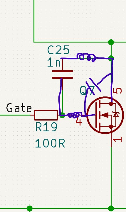
    In the last post, I mentioned how the MOSFET in the load stage, which is supposed to turn on and off the load resistor, was oscillating. I've been looking in to this more and I think I understand what I did to create the issue, even if I don't fully understand exactly how the oscillator I managed to create works.

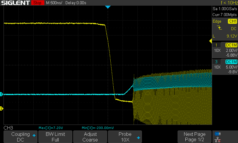
    Turn-off waveform with 1nF capacitor gate-drain. Yellow = gate-source voltage, Blue = drain-source voltage. It will oscillate indefinitely even with FET_EN signal to the gate drive removed. Oscillating at about 72MHz.

    I present to you, our culprit:

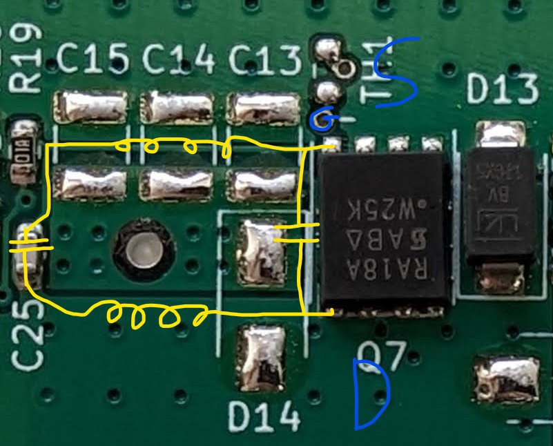
    Do you see it? While it might look like an innocent trace, it is really an inductor in disguise.

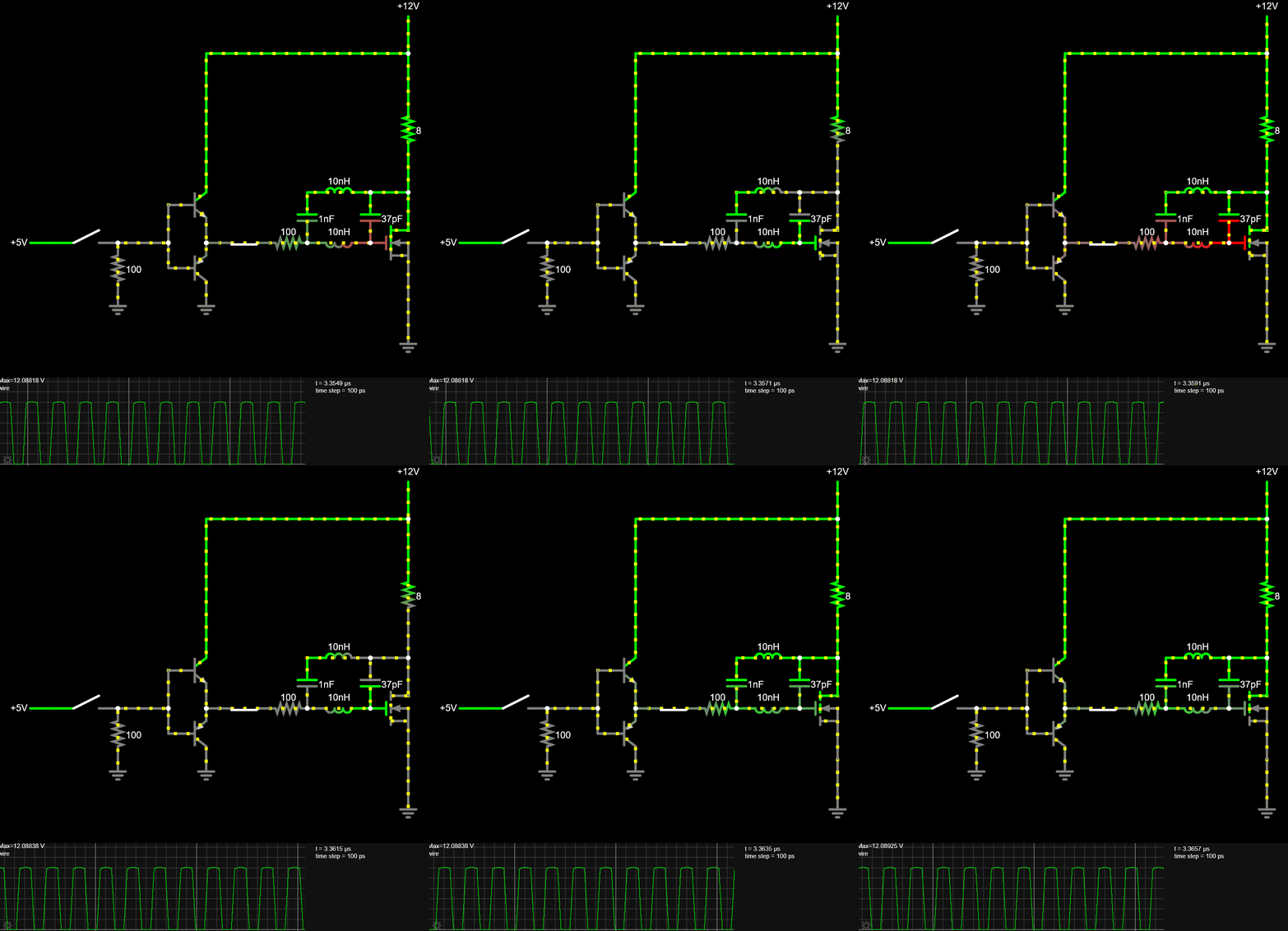
    I believe the capacitor I added, Cgd (C25), the gate-drain capacitance inside the MOSFET, the parasitic inductance of the traces, and the amplification of the MOSFET, have formed an oscillator.

    If you run the numbers, 1nF cap + 12nH inductance (ballpark guess) resonates at 46MHz, which is at least in the same order of magnitude as the 72MHz I'm measuring.

    The gate-drain cap was added in the first place to slow down the MOSFETs turn-off transition. This lowers the slew rate of the drain-source voltage, which slows down how quickly current must stop flowing through the inductance of the cables and load resistor (dI/dt), which thus reduces the inductive voltage spike across the MOSFET. However, in exchange more power is dissipated in the MOSFETs when switching. This cap, combined with the other mitigation strategies I'll describe in the future (RC snubber, TVS diodes, flyback diodes), should be enough to manage the inductive spikes for the 8R to 0.5R load stages (Currents 1.5-24A). The 0.1R load stage that will operate at 120A needs something a bit more special.

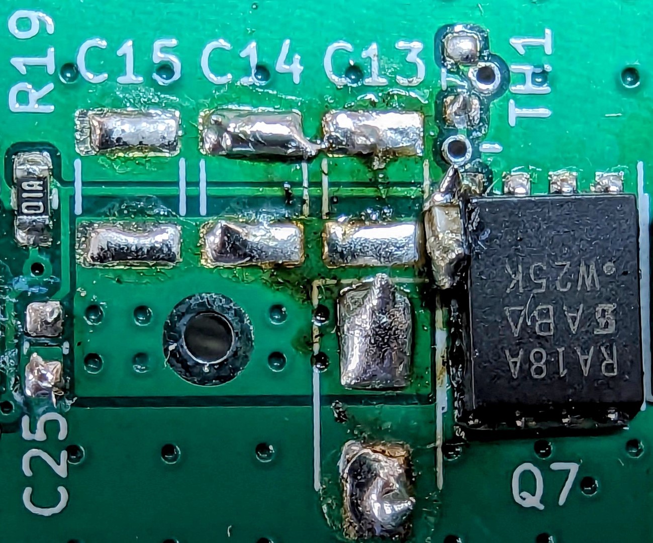
    To test this and remove nearly all of the trace parasitic inductance, I managed to cram the gate-drain capacitor right next to the MOSFET and solder it in. One end of the capacitor is actually soldered to the small bit of exposed drain terminal that sticks out the side of the MOSFET package.

    I don't think it's possible to get any lower inductance than this. The reason I didn't do this during the PCB layout is that I prioritized the trace inductance from the MOSFET to its TVS, and to the large capacitors used in the inductive energy capture circuit for the 0.1R load stage variant.

    Not pretty, but functional

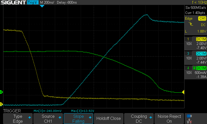
    The result is very good:

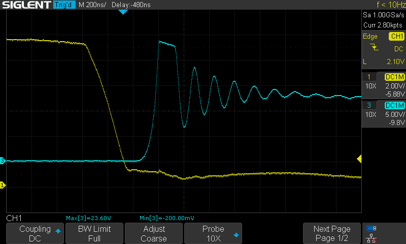
    Turn-off waveform with 1nF gate-drain capacitor and fixed parasitics. Yellow = gate-source voltage, Blue is drain-source voltage. Green is current through a current clamp to the entire load stage. Look how linear the voltage increase across the FET is! Overshoot is minimal at 13.92V on a 12.2V supply. 22nF + 10R snubber also present.

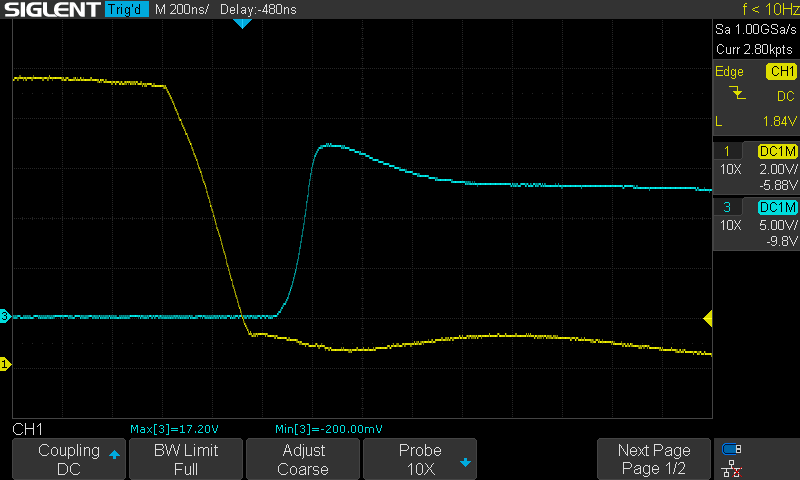
    For comparison, here is the turn-off waveform with no gate-drain capacitor:

    No gate-drain capacitor. RC snubber still present. Same time scale but different voltage scale on blue trace; it'd look even worse with the same voltage scale. Look how much steeper the dV/dt on the drain-source voltage is! Overshoot is now 17.2V.

    Just for fun, here is the waveform with no RC snubber. I believe the ringing is the inductance of the cables (700nH-ish?), the C_oss capacitance of the MOSFET (264pF), and the capacitance of the TVS (900pF). It rings at 6 MHz which is quite close to the 5.6 MHz I calculate for those values. :

    No gate-drain capacitor or RC snubber. Overshoot is 23.6V and that's only because it is clamped by the TVS.

    Although it feels less elegant, I'm probably going to leave the gate-drain capacitor off of the next load stages I assemble, and I'll try increasing the gate resistor to 3.3k to slow down the transition speed instead. Simulation shows that should work about the same. On a future revision of the load stage PCB, I'll add a footprint to put a gate-drain cap right next to the FET.

    Next up: why is there such a long 30us delay between the FET_EN logic signal going low, and the gate drive circuit output going low? I'm kind of regretting...

    Read more »
  • First Load Stage Testing

    tinfever06/27/2023 at 03:20 0 comments

    It's alive! Testing of the first load stage has begun. I'm starting with the 8R load stage to start small, and then I'll work my way up.

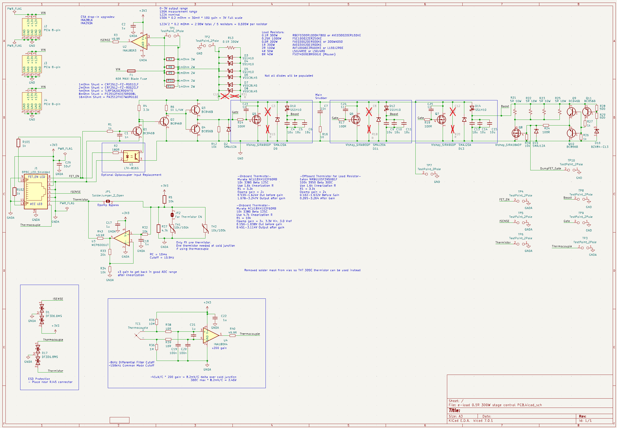
    Here is the current schematic of the load stage, in case anyone is curious. The same PCB is designed to support load resistors from 8R to 0.1R (thus currents from 1.5A - 122A) with different component configurations. KiCad doesn't have a good system for handling variants so you can't tell from the schematic which components I've loaded for this 8R load stage. I have the variant details in various part fields which does sort-of integrate with the interactive BOM generator though. The important variant details are: only one FET is populated as a SIRA18ADP, only one SS1H10 flyback diode, the "boost" section isn't loaded, and a single 16 mOhm current shunt.

    Overall, it's working well with the exception of two issues.

    1. When I started ramping up the voltage across the load, above about 10.5V, it would start to oscillate at a frequency of around 72 MHz on the turn-off transition. It was bad enough that it wasn't actually turning off at all. I don't fully understand it, but I believe this was due to a capacitor I added between the MOSFET gate and drain in order to slow the turn-off fall-time to reduce the inductive overshoot. I think during turn-off as the voltage across the FET started to rise, current was flowing through that cap causing the gate to rise as well, which turned the FET on so the voltage across it falls, until the gate driver has discharge the gate enough that the FET starts turning off again and the cycle repeats. I believe this is called dV/dT turn on, and I've exacerbated it by adding that cap (C25). Removing the cap fixed the issue, and the inductive spike overshoot is quite manageable right now (14.6V on a 12.2V supply). I'm curious if there is a way to fix it without removing that cap though.
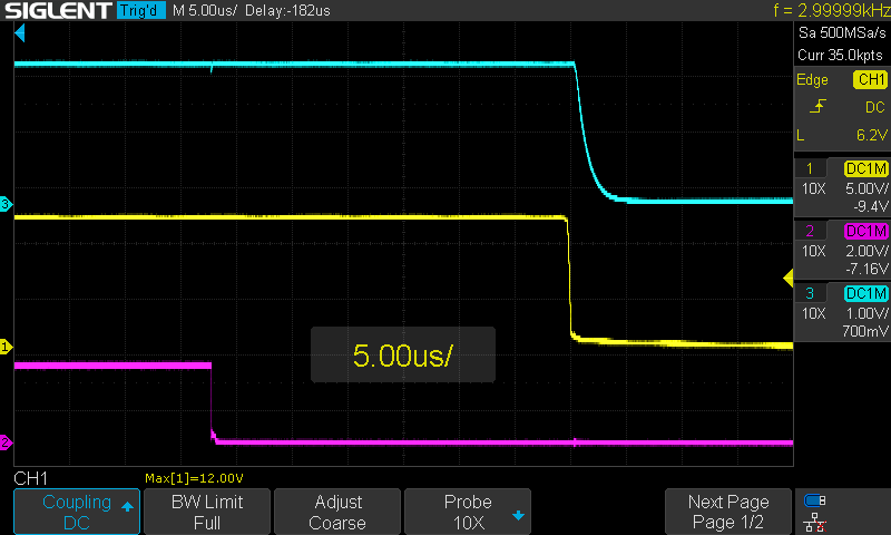
    2. There is a 30us delay between the FET_EN signal going low, and the FET gate actually going low. I need to look in to this more. I'm suspecting the optocoupler might be causing this. I know optocouplers can be slow but I didn't think they would be that slow. In theory, I could compensate for the turn-off delay in software, but I have a hunch it won't be consistent over all load input voltages since the load input is actually used to power the gate drivers and opto pull-up.

    Remaining to be tested:

    • Thermocouple amplifier. I'm trying to be clever and use a current sense amplifier as a differential thermocouple amplifier since they are very cheap and have very low offset voltages. It remains to be seen whether that is clever or foolish.
    • Current sense amplifier accuracy and offset
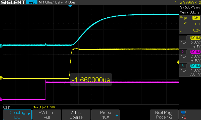
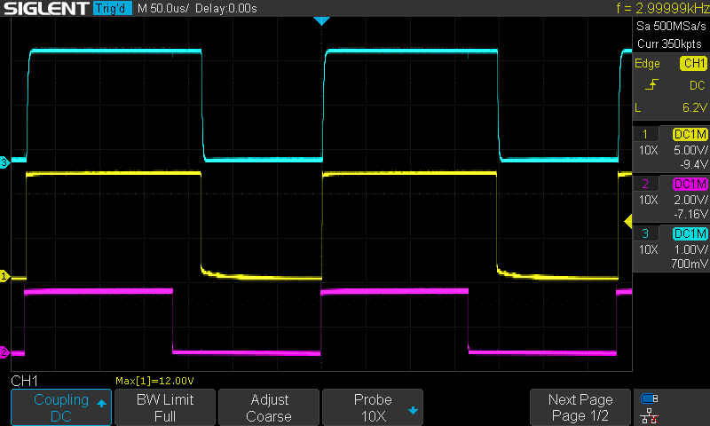
    Bottom signal is FET_EN, middle signal is gate voltage, top signal is I_SENSE output. Running at 3kHz no problem, except for turn-off delay.
    Turn-on time is reasonable and expected at around 2us. The current rises faster than shown here because the current sense amp is limited to 150kHz bandwidth.

    Turn-off delay shown here between FET_EN and gate voltage is quite bad at roughly 35us.

View all 11 project logs

  • 1
    Please refer to uploaded files for detailed build instructions and BOM

View all instructions

Enjoy this project?

Share

Discussions

john.r.sheahan wrote 07/14/2023 at 23:16 point

Hi, you might like to consider adding some control of di/dt, or how fast this load switches on and off to whatever current is selected. Big power supplies tend to be slow. Your early traces show the supply you use initially sourcing from output capacitance, that running out of charge, and then the supply control loop slowly catching up. 

For testing a supply, you probably want to see how the supply works when the load switches on and off more slowly than the supply voltage control loop.   Then later investigate what happens when the load switches quickly.  

  Are you sure? yes | no

tinfever wrote 07/15/2023 at 01:34 point

Do you mean di/dt control on the individual load stages or of the entire system? I think doing it at the entire system level should be possible by just enabling and disabling the load stages in the correct sequence to create a ramp. Although the slew rate between steps of the ramp would still be uncontrolled. There is probably a grey area where the desired ramp is too fast to use every "bit" of resolution, but you still don't want it so fast as turning all the applicable load stages on at once. In that case it wouldn't have much control.

Controlling that at the load stage would be much trickier I think. I'm not even entirely sure how you'd do that. Presumably it needs to be configurable on the fly, so it can't just be hardware. I think you'd have to redesign the load stage MOSFETs to be driven by opamps with current feedback, just like the normal electronic load designs, and then feed the opamps with a ramp signal. I couldn't just have a DAC signal for each load stage, so I think I'd have to somehow feed the same ramp signal to each load stage and have them scale it properly. Or maybe have some sort of voltage to ramp slope converter on each load stage so then the correct slew rate is loaded and stored on each load stage ahead of time, and then they can still be triggered to turn on by the FET_EN signal. This is probably all way too complicated though, and it was already borderline whether my current design is that much better than the usual linear FET electronic load design.

Thanks for the tip about the bench PSU control loop causing that odd waveform I was seeing. I looked in to it and it looks like the Korad PSUs might actually be running their control loop in software, which might explain why it is slow. For one of the tests I want to use this electronic load for, I actually want to be able to do current ramps at 40A/us. I'm not 100% sure I'll be able to do it though.

  Are you sure? yes | no

john.r.sheahan wrote 07/15/2023 at 02:07 point

Hi

I guess how many controlled places depends on how you plan to use it, but di/dt control on the larger current loads you plan to switch should help reasonable outputs without wierd voltage dips. Perhaps just fast and slow di/dt edge rates would do, where fast is defined by how much current you can drive into the gates of the switching mosfets to slew their input (and miller) capacitance. 

You could slow the edges by reducing the available current drive to the gate, or by padding the gate with additional capacitance. Either way could just be a 2 position switch, say fast, slow, and add medium if you really wanted.   Could be a switch, or opamp feedback, or current mirrors.  I'd suggest not actually doing active current feedback - it _will_ go unstable on some sources. 

  Are you sure? yes | no

tinfever wrote 07/16/2023 at 00:00 point

John, I can't reply to your latest comment since Hackaday.io doesn't seem to support nesting any more replies so I hope you'll see this somehow.

On your comment, those are good ideas on way to control it. Much simpler to have two modes than what I was thinking. Although, I think I'm probably going to see if I can get away without any additional slew rate control for now. There is already a capacitor added from gate-drain on the FETs to manage the inductive spike, but that's only really for the turn-off transition. I think trying to slow the current slew rate anymore, at the 3kHz pulse rate I'm targeting, would heat the the FETs up too much.

  Are you sure? yes | no

Kevin Kessler wrote 06/30/2023 at 04:21 point

10kW is ALOT of heat to get rid of. You might want to couple this project with one of those mini-foundry projects.

  Are you sure? yes | no

tinfever wrote 06/30/2023 at 16:39 point

Haha you're not wrong. I'm planning on putting the back right up to a window so all the heat can exhaust directly outside...hopefully not accidentally melting my window screen in the process. I am concerned about running the 300W resistors at full power since they definitely would overheat without airflow, and I'm not sure how much airflow they'll need. If I recall correctly, I think I did test one of the 300W resistors at full power with a box fan for air flow and that was enough to keep it from overheating, although I found the temperature coefficient of resistance seemed to be much higher than the datasheet indicated.

  Are you sure? yes | no

Dan Maloney wrote 06/23/2023 at 17:00 point

30 kW? I'm intrigued. Hope to see details on this one soon!

  Are you sure? yes | no

Similar Projects

Does this project spark your interest?

Become a member to follow this project and never miss any updates