The trickiest part of this electronics is the power management...
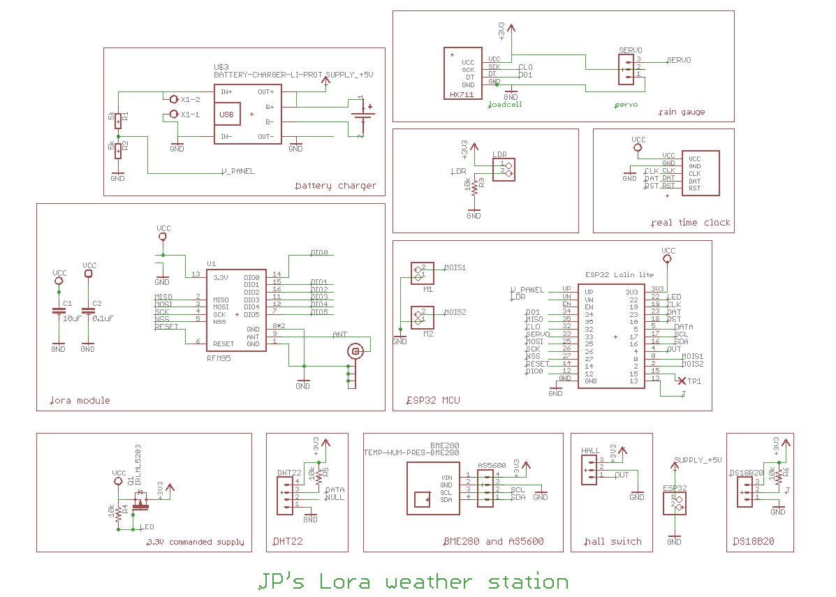
The first schematics was quite simple:
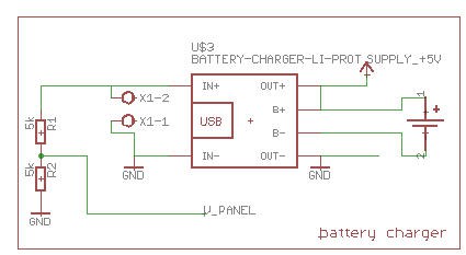
- As usual a TP4056 chip was used to charge the 18650 Li-ion battery
- Then in order to save battery during ESP32's deepsleep I added a P mosfet to cut power
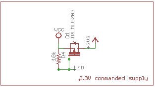
And here came the first problems... This Mosfet was working rather well and, as expected, allowed to switch off most of the sensors during deepSleep.
But, when switching On, the current flow added to the ESP32's voltage regulator was too high (from time to time) for this weak voltage reg ... VCC and 3.3V dropped and ESP32 started to stall (best case) and even to reboot in worst conditions.
Looking at the ESP32 lolin board schematics I found the culprit : ME6211C33M5G regulator is limited to 500mA output current...
So I had to modify a little the board to add a second voltage regulator which will be used only for powering the sensors.
The idea was to keep a ME6211 to take benefit of the "Enable" pin of this chip. So that it would replace the P-Mosfet of the first schematics and allow to "deepSleep" the sensors.
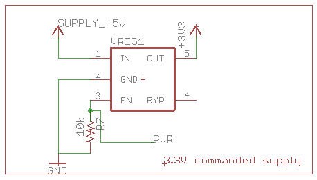
R7 resistor acts to pull down the enable pin, when PWR signal is floating (ESP32 into deepsleep) then the VREG1 chip is off. When PWR pin is at "high" state then the VREG1 outputs 3.3V --> nice !
This has been tested on the first version of my PCb's after a quick and dirty patch...
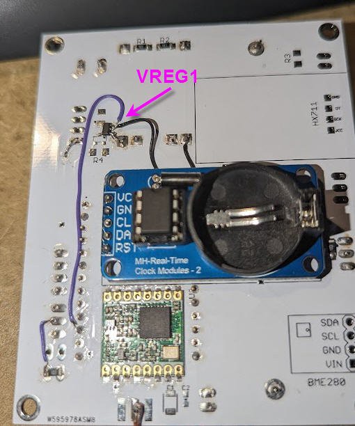
This patch has proven to work. But the V1 PCB was now "ugly"... So I asked PCBWay to help me once more !
And here is the final schematics:
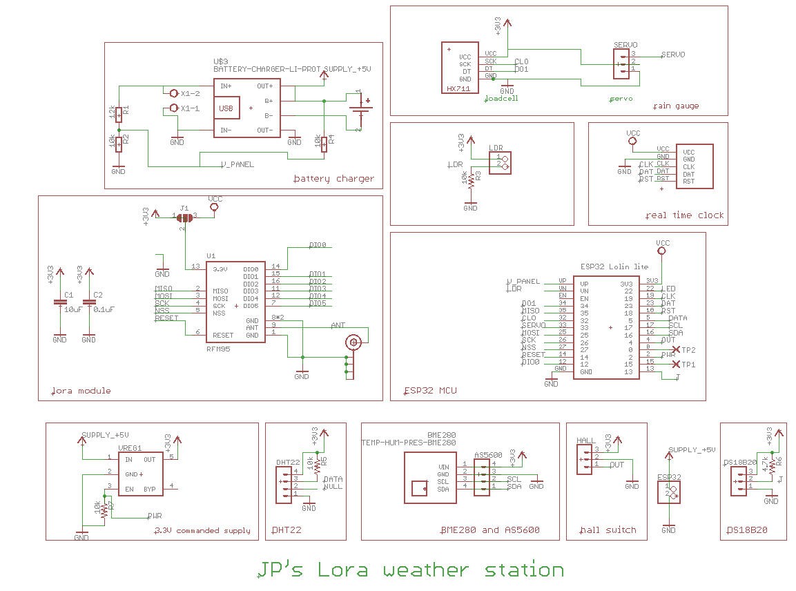
The rest of this schematics is self explainatory and is the same between V1 and V2. However you should be careful with the following details:
- V_PANEL can be used to monitor solar panel voltage via the R1/R2 voltage divider. In this configuration you MUST NOT solder R4 resistor
- V-PANEL can be used to monitor battery voltage via the voltage divider R4/R2. In this configuration you MUST NOT solder R1 resistor.
- J1 solder pad is, by default, sending VREG1 output to the Lora RFM95 chip. if you prefer to always power this module then cut J1 "left side" and bridge J1 "right side". RFM95 module would then be powered by ESP32 voltage regulator. (this can be useful for the GTW0 board (see later).
 JP Gleyzes
Discussions
Become a Hackaday.io Member
Create an account to leave a comment. Already have an account? Log In.